Semiconductor device and method for producing the same
US20140138852A1
2014-05-22
14/083,834
2013-11-19
✅ Patent granted
US 9,093,393 B2
2015-07-28
-
-
A. Sefer
2033-11-19
Abstract:
A semiconductor device includes a rectangular lower semiconductor element; a plurality of external electrodes located in a pattern on the lower semiconductor element along sides thereof; a plurality of internal electrodes electrically connected to the plurality of external electrodes via a plurality of line patterns respectively and located on the lower semiconductor element in a pattern; dams provided in such a pattern that each of the dams encloses one or at least two external electrodes among the plurality of external electrodes; an upper semiconductor element mounted on the lower semiconductor element such that a plurality of terminals on the upper semiconductor element are electrically connected to the plurality of internal electrodes respectively; and a resin potted to flow to a space between the lower semiconductor element and the upper semiconductor element.
Assignee:
- J-DEVICES CORPORATION 11 🇯🇵 Usuki, Japan
Applicant:
Interested in similar patents?
Get notified when new applications in this technology area are published.
Classification:
H01L23/3157 » CPC main
Details of semiconductor or other solid state devices; Encapsulations, e.g. encapsulating layers, coatings, e.g. for protection characterised by the arrangement or shape Partial encapsulation or coating
H01L21/563 » CPC further
Processes or apparatus adapted for the manufacture or treatment of semiconductor or solid state devices or of parts thereof; Manufacture or treatment of semiconductor devices or of parts thereof the devices having at least one potential-jump barrier or surface barrier, e.g. PN junction, depletion layer or carrier concentration layer; Assembly of semiconductor devices using processes or apparatus not provided for in a single one of the subgroups - , e.g. sealing of a cap to a base of a container; Encapsulations, e.g. encapsulation layers, coatings Encapsulation of active face of flip-chip device, e.g. underfilling or underencapsulation of flip-chip, encapsulation preform on chip or mounting substrate
H01L23/147 » CPC further
Details of semiconductor or other solid state devices; Mountings, e.g. non-detachable insulating substrates characterised by the material or its electrical properties Semiconductor insulating substrates
H01L23/49833 » CPC further
Details of semiconductor or other solid state devices; Arrangements for conducting electric current to or from the solid state body in operation, e.g. leads, terminal arrangements ; Selection of materials therefor consisting of soldered constructions; Leads, on insulating substrates, the chip support structure consisting of a plurality of insulating substrates
H01L23/49838 » CPC further
Details of semiconductor or other solid state devices; Arrangements for conducting electric current to or from the solid state body in operation, e.g. leads, terminal arrangements ; Selection of materials therefor consisting of soldered constructions; Leads, on insulating substrates, Geometry or layout
H01L24/05 » CPC further
Arrangements for connecting or disconnecting semiconductor or solid-state bodies; Methods or apparatus related thereto; Means for bonding being attached to, or being formed on, the surface to be connected, e.g. chip-to-package, die-attach, "first-level" interconnects; Manufacturing methods related thereto; Bonding areas ; Manufacturing methods related thereto; Structure, shape, material or disposition of the bonding areas prior to the connecting process of an individual bonding area
H01L24/06 » CPC further
Arrangements for connecting or disconnecting semiconductor or solid-state bodies; Methods or apparatus related thereto; Means for bonding being attached to, or being formed on, the surface to be connected, e.g. chip-to-package, die-attach, "first-level" interconnects; Manufacturing methods related thereto; Bonding areas ; Manufacturing methods related thereto; Structure, shape, material or disposition of the bonding areas prior to the connecting process of a plurality of bonding areas
H01L24/32 » CPC further
Arrangements for connecting or disconnecting semiconductor or solid-state bodies; Methods or apparatus related thereto; Means for bonding being attached to, or being formed on, the surface to be connected, e.g. chip-to-package, die-attach, "first-level" interconnects; Manufacturing methods related thereto; Layer connectors, e.g. plate connectors, solder or adhesive layers; Manufacturing methods related thereto; Structure, shape, material or disposition of the layer connectors after the connecting process of an individual layer connector
H01L24/92 » CPC further
Arrangements for connecting or disconnecting semiconductor or solid-state bodies; Methods or apparatus related thereto; Methods for connecting semiconductor or solid state bodies including different methods provided for in two or more of groups - Specific sequence of method steps
H01L25/00 » CPC further
Assemblies consisting of a plurality of individual semiconductor or other solid state devices ; Multistep manufacturing processes thereof
H01L25/0657 » CPC further
Assemblies consisting of a plurality of individual semiconductor or other solid state devices ; Multistep manufacturing processes thereof all the devices being of a type provided for in the same subgroup of groups - , e.g. assemblies of rectifier diodes the devices not having separate containers the devices being of a type provided for in group Stacked arrangements of devices
H01L25/50 » CPC further
Assemblies consisting of a plurality of individual semiconductor or other solid state devices ; Multistep manufacturing processes thereof Multistep manufacturing processes of assemblies consisting of devices, each device being of a type provided for in group or
H01L23/3128 » CPC further
Details of semiconductor or other solid state devices; Encapsulations, e.g. encapsulating layers, coatings, e.g. for protection characterised by the arrangement or shape the device being completely enclosed a substrate forming part of the encapsulation the substrate having spherical bumps for external connection
H01L23/49827 » CPC further
Details of semiconductor or other solid state devices; Arrangements for conducting electric current to or from the solid state body in operation, e.g. leads, terminal arrangements ; Selection of materials therefor consisting of soldered constructions; Leads, on insulating substrates, Via connections through the substrates, e.g. pins going through the substrate, coaxial cables
H01L23/556 » CPC further
Details of semiconductor or other solid state devices; Protection against radiation, e.g. light or electromagnetic waves against alpha rays
H01L24/29 » CPC further
Arrangements for connecting or disconnecting semiconductor or solid-state bodies; Methods or apparatus related thereto; Means for bonding being attached to, or being formed on, the surface to be connected, e.g. chip-to-package, die-attach, "first-level" interconnects; Manufacturing methods related thereto; Layer connectors, e.g. plate connectors, solder or adhesive layers; Manufacturing methods related thereto; Structure, shape, material or disposition of the layer connectors prior to the connecting process of an individual layer connector
H01L24/48 » CPC further
Arrangements for connecting or disconnecting semiconductor or solid-state bodies; Methods or apparatus related thereto; Means for bonding being attached to, or being formed on, the surface to be connected, e.g. chip-to-package, die-attach, "first-level" interconnects; Manufacturing methods related thereto; Wire connectors; Manufacturing methods related thereto; Structure, shape, material or disposition of the wire connectors after the connecting process of an individual wire connector
H01L24/73 » CPC further
Arrangements for connecting or disconnecting semiconductor or solid-state bodies; Methods or apparatus related thereto Means for bonding being of different types provided for in two or more of groups , , , , , , ,
H01L24/81 » CPC further
Arrangements for connecting or disconnecting semiconductor or solid-state bodies; Methods or apparatus related thereto; Methods for connecting semiconductor or other solid state bodies using means for bonding being attached to, or being formed on, the surface to be connected using a bump connector
H01L24/94 » CPC further
Arrangements for connecting or disconnecting semiconductor or solid-state bodies; Methods or apparatus related thereto; Batch processes at wafer-level, i.e. with connecting carried out on a wafer comprising a plurality of undiced individual devices
H01L2224/0226 » CPC further
Indexing scheme for arrangements for connecting or disconnecting semiconductor or solid-state bodies and methods related thereto as covered by; Means for bonding being attached to, or being formed on, the surface to be connected, e.g. chip-to-package, die-attach, "first-level" interconnects; Manufacturing methods related thereto; Bonding areas; Manufacturing methods related thereto; Auxiliary members for bonding areas, e.g. spacers being formed on the semiconductor or solid-state body not in direct contact with the bonding area Material of the auxiliary member
H01L2224/02245 » CPC further
Indexing scheme for arrangements for connecting or disconnecting semiconductor or solid-state bodies and methods related thereto as covered by; Means for bonding being attached to, or being formed on, the surface to be connected, e.g. chip-to-package, die-attach, "first-level" interconnects; Manufacturing methods related thereto; Bonding areas; Manufacturing methods related thereto; Auxiliary members for bonding areas, e.g. spacers being formed on the semiconductor or solid-state body not in direct contact with the bonding area Flow barrier
H01L2224/02255 » CPC further
Indexing scheme for arrangements for connecting or disconnecting semiconductor or solid-state bodies and methods related thereto as covered by; Means for bonding being attached to, or being formed on, the surface to be connected, e.g. chip-to-package, die-attach, "first-level" interconnects; Manufacturing methods related thereto; Bonding areas; Manufacturing methods related thereto; Auxiliary members for bonding areas, e.g. spacers being formed on the semiconductor or solid-state body not in direct contact with the bonding area Shape of the auxiliary member
H01L2224/0401 » CPC further
Indexing scheme for arrangements for connecting or disconnecting semiconductor or solid-state bodies and methods related thereto as covered by; Means for bonding being attached to, or being formed on, the surface to be connected, e.g. chip-to-package, die-attach, "first-level" interconnects; Manufacturing methods related thereto; Bonding areas; Manufacturing methods related thereto; Structure, shape, material or disposition of the bonding areas prior to the connecting process Bonding areas specifically adapted for bump connectors, e.g. under bump metallisation [UBM]
H01L2224/04042 » CPC further
Indexing scheme for arrangements for connecting or disconnecting semiconductor or solid-state bodies and methods related thereto as covered by; Means for bonding being attached to, or being formed on, the surface to be connected, e.g. chip-to-package, die-attach, "first-level" interconnects; Manufacturing methods related thereto; Bonding areas; Manufacturing methods related thereto; Structure, shape, material or disposition of the bonding areas prior to the connecting process Bonding areas specifically adapted for wire connectors, e.g. wirebond pads
H01L2224/06051 » CPC further
Indexing scheme for arrangements for connecting or disconnecting semiconductor or solid-state bodies and methods related thereto as covered by; Means for bonding being attached to, or being formed on, the surface to be connected, e.g. chip-to-package, die-attach, "first-level" interconnects; Manufacturing methods related thereto; Bonding areas; Manufacturing methods related thereto; Structure, shape, material or disposition of the bonding areas prior to the connecting process of a plurality of bonding areas; Shape Bonding areas having different shapes
H01L2224/11462 » CPC further
Indexing scheme for arrangements for connecting or disconnecting semiconductor or solid-state bodies and methods related thereto as covered by; Means for bonding being attached to, or being formed on, the surface to be connected, e.g. chip-to-package, die-attach, "first-level" interconnects; Manufacturing methods related thereto; Bump connectors; Manufacturing methods related thereto; Manufacturing methods by blanket deposition of the material of the bump connector; Plating Electroplating
H01L2224/26145 » CPC further
Indexing scheme for arrangements for connecting or disconnecting semiconductor or solid-state bodies and methods related thereto as covered by; Means for bonding being attached to, or being formed on, the surface to be connected, e.g. chip-to-package, die-attach, "first-level" interconnects; Manufacturing methods related thereto; Layer connectors, e.g. plate connectors, solder or adhesive layers; Manufacturing methods related thereto; Auxiliary members for layer connectors, e.g. spacers being formed on the semiconductor or solid-state body to be connected Flow barriers
H01L2224/26175 » CPC further
Indexing scheme for arrangements for connecting or disconnecting semiconductor or solid-state bodies and methods related thereto as covered by; Means for bonding being attached to, or being formed on, the surface to be connected, e.g. chip-to-package, die-attach, "first-level" interconnects; Manufacturing methods related thereto; Layer connectors, e.g. plate connectors, solder or adhesive layers; Manufacturing methods related thereto; Auxiliary members for layer connectors, e.g. spacers being formed on an item to be connected not being a semiconductor or solid-state body Flow barriers
H01L2224/73204 » CPC further
Indexing scheme for arrangements for connecting or disconnecting semiconductor or solid-state bodies and methods related thereto as covered by; Means for bonding being of different types provided for in two or more of groups; Location after the connecting process on the same surface; Bump and layer connectors the bump connector being embedded into the layer connector
H01L2224/73207 » CPC further
Indexing scheme for arrangements for connecting or disconnecting semiconductor or solid-state bodies and methods related thereto as covered by; Means for bonding being of different types provided for in two or more of groups; Location after the connecting process on the same surface Bump and wire connectors
H01L2224/73265 » CPC further
Indexing scheme for arrangements for connecting or disconnecting semiconductor or solid-state bodies and methods related thereto as covered by; Means for bonding being of different types provided for in two or more of groups; Location after the connecting process on different surfaces Layer and wire connectors
H01L2224/81193 » CPC further
Indexing scheme for arrangements for connecting or disconnecting semiconductor or solid-state bodies and methods related thereto as covered by; Methods for connecting semiconductor or other solid state bodies using means for bonding being attached to, or being formed on, the surface to be connected using a bump connector; Arrangement of the bump connectors prior to mounting wherein the bump connectors are disposed on both the semiconductor or solid-state body and another item or body to be connected to the semiconductor or solid-state body
H01L2224/92125 » CPC further
Indexing scheme for arrangements for connecting or disconnecting semiconductor or solid-state bodies and methods related thereto as covered by; Methods for connecting semiconductor or solid state bodies including different methods provided for in two or more of groups - ; Specific sequence of method steps; Connecting a surface with connectors of different types; Sequential connecting processes the first connecting process involving a bump connector the second connecting process involving a layer connector
H01L2224/92225 » CPC further
Indexing scheme for arrangements for connecting or disconnecting semiconductor or solid-state bodies and methods related thereto as covered by; Methods for connecting semiconductor or solid state bodies including different methods provided for in two or more of groups - ; Specific sequence of method steps; Connecting different surfaces of the semiconductor or solid-state body with connectors of different types; Sequential connecting processes the first connecting process involving a bump connector the second connecting process involving a layer connector
H01L2224/92247 » CPC further
Indexing scheme for arrangements for connecting or disconnecting semiconductor or solid-state bodies and methods related thereto as covered by; Methods for connecting semiconductor or solid state bodies including different methods provided for in two or more of groups - ; Specific sequence of method steps; Connecting different surfaces of the semiconductor or solid-state body with connectors of different types; Sequential connecting processes the first connecting process involving a layer connector the second connecting process involving a wire connector
H01L2224/94 » CPC further
Indexing scheme for arrangements for connecting or disconnecting semiconductor or solid-state bodies and methods related thereto as covered by; Batch processes at wafer-level, i.e. with connecting carried out on a wafer comprising a plurality of undiced individual devices
H01L2225/0651 » CPC further
Details relating to assemblies covered by the group but not provided for in its subgroups; All the devices being of a type provided for in the same subgroup of groups - the devices not having separate containers the devices being of a type provided for in group; Stacked arrangements of devices Wire or wire-like electrical connections from device to substrate
H01L2225/06513 » CPC further
Details relating to assemblies covered by the group but not provided for in its subgroups; All the devices being of a type provided for in the same subgroup of groups - the devices not having separate containers the devices being of a type provided for in group; Stacked arrangements of devices Bump or bump-like direct electrical connections between devices, e.g. flip-chip connection, solder bumps
H01L2225/06568 » CPC further
Details relating to assemblies covered by the group but not provided for in its subgroups; All the devices being of a type provided for in the same subgroup of groups - the devices not having separate containers the devices being of a type provided for in group; Stacked arrangements of devices; Geometry of the stack, e.g. form of the devices, geometry to facilitate stacking the devices decreasing in size, e.g. pyramidical stack
H01L2924/10253 » CPC further
Indexing scheme for arrangements or methods for connecting or disconnecting semiconductor or solid-state bodies as covered by; Details of semiconductor or other solid state devices to be connected; Material of the semiconductor or solid state bodies; Semiconducting materials; Elemental semiconductors, i.e. Group IV Silicon [Si]
H01L2924/14 » CPC further
Indexing scheme for arrangements or methods for connecting or disconnecting semiconductor or solid-state bodies as covered by; Details of semiconductor or other solid state devices to be connected; Device type Integrated circuits
H01L2924/157 » CPC further
Indexing scheme for arrangements or methods for connecting or disconnecting semiconductor or solid-state bodies as covered by; Details of package parts other than the semiconductor or other solid state devices to be connected; Die mounting substrate; Material with a principal constituent of the material being a metal or a metalloid, e.g. boron [B], silicon [Si], germanium [Ge], arsenic [As], antimony [Sb], tellurium [Te] and polonium [Po], and alloys thereof
H01L2924/15311 » CPC further
Indexing scheme for arrangements or methods for connecting or disconnecting semiconductor or solid-state bodies as covered by; Details of package parts other than the semiconductor or other solid state devices to be connected; Die mounting substrate; Connection portion the connection portion being formed only on the surface of the substrate opposite to the die mounting surface being a ball array, e.g. BGA
H01L2924/19107 » CPC further
Indexing scheme for arrangements or methods for connecting or disconnecting semiconductor or solid-state bodies as covered by; Details of hybrid assemblies other than the semiconductor or other solid state devices to be connected; Disposition of discrete passive components off-chip wires
H01L23/48 IPC
Details of semiconductor or other solid state devices Arrangements for conducting electric current to or from the solid state body in operation, e.g. leads, terminal arrangements ; Selection of materials therefor
H01L23/31 IPC
Details of semiconductor or other solid state devices; Encapsulations, e.g. encapsulating layers, coatings, e.g. for protection characterised by the arrangement or shape
H01L21/56 IPC
Processes or apparatus adapted for the manufacture or treatment of semiconductor or solid state devices or of parts thereof; Manufacture or treatment of semiconductor devices or of parts thereof the devices having at least one potential-jump barrier or surface barrier, e.g. PN junction, depletion layer or carrier concentration layer; Assembly of semiconductor devices using processes or apparatus not provided for in a single one of the subgroups - , e.g. sealing of a cap to a base of a container Encapsulations, e.g. encapsulation layers, coatings
H01L23/00 IPC
Details of semiconductor or other solid state devices
H01L25/065 IPC
Assemblies consisting of a plurality of individual semiconductor or other solid state devices ; Multistep manufacturing processes thereof all the devices being of a type provided for in the same subgroup of groups - , e.g. assemblies of rectifier diodes the devices not having separate containers the devices being of a type provided for in group
H01L23/14 IPC
Details of semiconductor or other solid state devices; Mountings, e.g. non-detachable insulating substrates characterised by the material or its electrical properties
H01L23/498 IPC
Details of semiconductor or other solid state devices; Arrangements for conducting electric current to or from the solid state body in operation, e.g. leads, terminal arrangements ; Selection of materials therefor consisting of soldered constructions Leads, on insulating substrates,
Description
CROSS REFERENCE TO RELATED APPLICATION
This application is based upon and claims the benefit of priority from the prior Japanese Patent Application No. 2012-253070, filed on Nov. 19, 2012; the entire contents of which are incorporated herein by reference.
FIELD
The present invention relates to a semiconductor device and a method for producing the same. Specifically, the present invention relates to a highly reliable semiconductor device of a CoC (chip-on-chip) structure which prevents an underfill resin from flowing into an external electrode (peripheral electrode) of a lower semiconductor element regardless of the size of an upper semiconductor element, and a method for producing the same.
BACKGROUND
Conventionally, a semiconductor device of a CoC (chip-on-chip) connection structure has been studied. With reference to FIG. 8, a specific structure of such a semiconductor device will be described. On a lower semiconductor chip 6 having external electrodes 9 formed on a surface thereof, an upper semiconductor chip 5 is mounted in a flip-flop manner with bumps 8 being held therebetween. A space between the lower semiconductor chip 6 and the upper semiconductor chip 5 and the bumps 8 are covered with an underfill resin 4 which has flown to the space as a result of being potted. The lower semiconductor chip 6 is mounted on a base substrate 2 with an adhesive 7 held therebetween, and the external electrodes 9 provided on a peripheral area of the lower semiconductor chip 6 and electrodes on the base substrate 2 are electrically connected to each other by bonding wires 10. On the base substrate 2, a resin 1 is provided to cover the upper semiconductor chip 5 and the lower semiconductor chip 6. On a rear surface of the base substrate 2, solder balls 3 are formed. The solder balls 3 are used for mounting the semiconductor device on a printed circuit board or the like.
The above-described semiconductor device of the CoC connection structure involves an undesirable possibility that the underfill resin 4 provided by potting flows onto surfaces of the external electrodes 9 and thus inhibits electrical contact between the external electrodes 9 and the bonding wires 10.
Japanese Laid-Open Patent Publication No. 2003-234362 (Patent Document 1) and Japanese Laid-Open Patent Publication No. 2005-276879 (Patent Document 2) each disclose a semiconductor device including a dam in order to prevent the underfill resin 4 provided by potting from reaching the surfaces of the external electrodes 9. A semiconductor device obtained by applying such a dam to the semiconductor device shown in FIG. 8 will be described with reference to FIGS. 9, 10 and 11.
FIG. 9 is a cross-sectional view of a semiconductor device including a dam 11 in order to prevent the underfill resin 4 provided by potting from reaching the surfaces of the external electrodes 9. FIG. 10 is a plan view of a lower semiconductor chip 6 of the semiconductor device shown in FIG. 9. FIG. 11 is a cross-sectional view of an upper semiconductor chip 5 and the lower semiconductor chip 6 of the semiconductor device shown in FIG. 9 which are immediately after being CoC-connected to each other. When the underfill resin 4 is potted to an area between the dam 11 and the upper semiconductor chip 5 in this state, the underfill resin 4 expands as shown in the cross-sectional view of FIG. 9. Even though flowing externally, the underfill resin 4 is stopped by the dam 11 to a certain extent. Therefore, the surfaces of the external electrodes 9 are not covered with the underfill resin 4. This decreases the possibility that the electrical contact between the external electrodes 9 and the bonding wires 10 is inhibited.
However, in the conventional semiconductor device of the CoC connection structure, once the underfill resin 4 flowing externally flows beyond the dam 11, the surfaces of many external electrodes 9 are covered with the underfill resin 4. This inhibits electrical contact between the external electrodes 9 and the bonding wires 10. In order to avoid such a problem, the dam 11 and the upper semiconductor chip 5 need to be located sufficiently far from each other, and the amount of the underfill resin 4 needs to be controlled precisely.
These prevent size reduction and mass production of the semiconductor device. In addition, in the conventional semiconductor device of the CoC connection structure, the dam 11 which encloses internal electrodes is formed of only one line. Such a dam 11 involves an undesirable possibility of being delaminated off during heat treatment or resin potting.
The present invention made in light of the above-described problems has an object of providing a semiconductor device of a CoC connection structure which does not inhibit electrical contact between external electrodes and line patterns and is not prevented from being reduced in size or from being mass-produced, and a method for producing such a semiconductor device.
SUMMARY
In order to solve the above-described problems, a semiconductor device in an embodiment according to the present invention includes a rectangular lower semiconductor element; a plurality of external electrodes located in a pattern on the lower semiconductor element along sides thereof; a plurality of internal electrodes electrically connected to the plurality of external electrodes via a plurality of line patterns respectively and located on the lower semiconductor element in a pattern; dams provided in such a pattern that each of the dams encloses one or at least two external electrodes among the plurality of external electrodes; an upper semiconductor element mounted on the lower semiconductor element such that a plurality of terminals on the upper semiconductor element are electrically connected to the plurality of internal electrodes respectively; and a resin potted to flow to a space between the lower semiconductor element and the upper semiconductor element.
It is preferable that the dams are formed of solder and are formed at the same time as solder bumps formed on the internal electrodes.
It is preferable that an insulating film is provided on a surface of the lower semiconductor element; the plurality of line patterns are provided on the insulating film; and an insulating thin film having openings positionally corresponding to the plurality of internal electrodes and the plurality of external electrodes is provided on the line patterns.
It is preferable that the dams have a gap therebetween, the gap extending from an area where the resin is potted to an external peripheral area of the lower semiconductor element.
It is preferable that at least one of the dams encloses at least two external electrodes among the plurality of external electrodes and extends between the at least two external electrodes.
In order to solve the above-described problems, a method for producing a semiconductor device in an embodiment according to the present invention includes the steps of: forming, on a rectangular lower semiconductor element, a plurality of external electrodes located in a pattern along sides of the lower semiconductor element, a plurality of internal electrodes located in a pattern, and line patterns for electrically connecting the plurality of external electrodes and the plurality of internal electrodes to each other respectively; forming dams such that each of the dams encloses one or at least two external electrodes among the plurality of external electrodes; mounting an upper semiconductor element on the lower semiconductor element such that a plurality of terminals on the upper semiconductor element are electrically connected to the plurality of internal electrodes respectively; and potting a resin such that the resin flows to a space between the lower semiconductor element and the upper semiconductor element.
It is preferable that the dams are formed of solder and are formed at the same time as solder bumps formed on the internal electrodes.
It is preferable that an insulating film is formed on a surface of the lower semiconductor element; the plurality of line patterns are formed on the insulating film; and an insulating thin film having openings positionally corresponding to the plurality of internal electrodes and the plurality of external electrodes is formed on the line patterns.
It is preferable that the dams are formed to have a gap therebetween, the gap extending from an area where the resin is to be potted to an external peripheral area of the lower semiconductor element.
It is preferable that the dams are formed such that at least one of the dams encloses at least two external electrodes among the plurality of external electrodes and extends between the at least two external electrodes.
The present invention provides a semiconductor device of a CoC connection structure which does not inhibit electrical contact between external electrodes and line patterns and is not prevented from being reduced in size or from being mass-produced, and a method for producing such a semiconductor device. Other effects of the present invention will be described below in detail.
BRIEF DESCRIPTION OF DRAWINGS
FIG. 1 is a cross-sectional view of a semiconductor device in an embodiment according to the present invention;
FIG. 2 is a plan view of a lower semiconductor chip in an embodiment according to the present invention;
FIG. 3 is a cross-sectional view of the lower semiconductor chip and an upper semiconductor chip in an embodiment according to the present invention before being CoC-connected to each other;
FIG. 4 is a cross-sectional view of the lower semiconductor chip and the upper semiconductor chip in an embodiment according to the present invention which are CoC-connected to each other;
FIG. 5 is a plan view of a lower semiconductor chip in a first modification of the embodiment according to the present invention;
FIG. 6 is a plan view of a lower semiconductor chip in a second modification of the embodiment according to the present invention;
FIG. 7 is a plan view of a lower semiconductor chip in a third modification of the embodiment according to the present invention;
FIG. 8 is a cross-sectional view of a conventional semiconductor device (with no dam);
FIG. 9 is a cross-sectional view of a conventional semiconductor device (with a dam);
FIG. 10 is a plan view of a lower semiconductor chip in the conventional semiconductor device; and
FIG. 11 is a cross-sectional view of the lower semiconductor chip and an upper semiconductor chip of the conventional semiconductor device which are CoC-connected to each other.
DESCRIPTION OF EMBODIMENTS
Hereinafter, embodiments according to the present invention will be described with reference to FIG. 1 through FIG. 7. In the embodiments, identical components will bear identical reference numerals and the same descriptions will not be repeated.
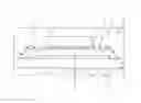
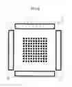
FIG. 1 is a cross-sectional view of a semiconductor device in an embodiment according to the present invention. The semiconductor device includes a lower semiconductor chip 6 mounted on a base substrate 2 and an upper semiconductor chip 5 mounted on the lower semiconductor chip 6 as main components.
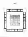
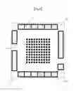
FIG. 2 is a plan view of the lower semiconductor chip 6 in an embodiment according to the present invention. The lower semiconductor chip 6 is rectangular, and external electrodes 9 are located on a surface of the lower semiconductor chip 6 along four sides thereof. In the figure, a plurality of external electrodes 9 are located in one line along each side. Alternatively, the external electrodes 9 may be located in two lines or in a staggered manner. Internal electrodes 80 are located in rows by columns on the lower semiconductor chip 6 and are electrically connected to the upper semiconductor chip 5.
Hereinafter, each of the components of the semiconductor device will be described along with the steps of production thereof.
The lower semiconductor chip 6 includes a silicon substrate, and may or may not have an integrated circuit formed on a surface thereof. In either case, an uppermost layer of the lower semiconductor chip 6 is, for example, a silicon nitride film. On the uppermost layer, the external electrodes 9, the internal electrodes 80 and lines (not shown) for connecting the external electrodes 9 and the internal electrodes 80 to each other are formed of a copper thin film. On these copper lines and the like, a polyimide insulating film having a thickness of 5 μm is formed in this example. The polyimide insulating film has openings for exposing the external electrodes 9, the internal electrodes 80 and dummy lines (on which dams 12 are to be formed) formed of a copper thin film. The dummy lines formed of a copper thin film may be formed at the same time as the external electrodes 9, the internal electrodes 80 and the lines for connecting the external electrodes 9 and the internal electrodes 80 to each other. The polyimide insulating film is applied by, for example, spin coating, and the openings are formed by etching. Formation of the polyimide insulating film can prevent damages of, for example, the lines formed of a copper thin film or the like for connecting the external electrodes 9 and the internal electrodes 80 to each other, and also can block a line, which causes a so-called soft error.
The internal electrodes 80 formed on the lower semiconductor chip 6 each have an aluminum pad of an optional shape, for example, an octagonal shape having a diameter of 20 μm. The internal electrodes 80 are located in, for example, 30 rows by 30 columns. The internal electrodes 80 are located at a pitch of, for example, 40 μm.
The external electrodes 9 on the surface of the lower semiconductor chip 6 are grouped, and each group of external electrodes 9 is located along one side of the lower semiconductor chip 6. Dams 12 are formed on the dummy lines of a copper thin film which are exposed by the openings of the polyimide insulating film. Each of the dams 12 encloses one group of external electrodes 9. Each dam 12 is formed in a ladder shape; namely, encloses the corresponding group of external electrodes 9 and also extends between adjacent external electrodes 9. The dams 12 are provided in such a pattern are separated from each other at positions in the vicinity of four corners of the lower semiconductor chip 6, and gaps 13 through which the underfill resin 4 flows to an external peripheral area of the lower semiconductor chip 6 are provided at these positions. The dams 12 are formed of solder, and each have a width of 45 μm to 55 μm and a height of 15 μm to 25 μm. More preferably, the dams 12 each have a width of 50 um and a height of 20 μm. On surfaces of the internal electrodes 80 also, solder layers 81 (shown in FIG. 3) are formed. The solder layers 81 are formed at the same time as the dams 12 by, for example, electrolytic plating with a barrier metal layer formed of nickel or the like being held between the internal electrodes 80 and the solder layers 81. The above description has been made regarding one lower semiconductor chip 6. In actuality, the solder layers 81 on the surfaces of the internal electrodes 80 and the dams 12 are formed on a wafer including a plurality of lower semiconductor chips 6. After this, the wafer is cut into individual lower semiconductor chips 6. Then, each lower semiconductor chip 6 is joined with the upper semiconductor chip 5, and the space between the lower semiconductor chip 6 and the upper semiconductor chip 5 is filled with the underfill resin 4, as described later.
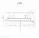
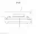
FIG. 3 is a cross-sectional view of the lower semiconductor chip 6 and the upper semiconductor chip 5 in an embodiment according to the present invention before being CoC-connected to each other. From the surface of the lower semiconductor chip 6, the dams 12 formed of solder and solder layers 81 formed of solder on the surfaces of the internal electrodes 80 protrude upward. On a surface electrode of the upper semiconductor chip 5 which already has an integrated circuit formed thereon, solder layers 82 are formed. The solder layers 81 and the solder layers 82 are positionally aligned, and thus the upper semiconductor chip 5 and the lower semiconductor chip 6 are CoC-connected to each other. The heating temperature in this step is about 260° C., which is higher than the melting point of solder. Therefore, the solder layers 81 and the solder layers 82 are fused and bonded together. As a result, as shown in FIG. 4, drumstick-like bumps 8 are formed.
In the state where the CoC-connected upper semiconductor chip 5 and lower semiconductor chip 6 are kept at about 100° C., the underfill resin 4 is potted to an area between the upper semiconductor chip 5 and the dams 12. As the underfill resin 4, an epoxy resin is used. As a result, the space between the lower semiconductor chip 6 and the upper semiconductor chip 5 is filled with the underfill resin 4 and the bumps 8 are covered with the underfill resin 4, because of the surface tension of the underfill resin 4 (see FIG. 1). Even if the underfill resin 4 is about to overflow top surfaces of the dams 12 for a reason that the amount of the underfill resin 4 is too large or the distance between the dams 12 and the upper semiconductor chip 5 is too short, the underfill resin 4 escapes to the external peripheral area of the lower semiconductor chip 6 via the gaps 13. Therefore, the underfill resin 4 does not flow onto the external electrodes 9. In addition, since the dams 12 enclose the external electrodes 9, the underfill resin 4 which has escaped to the external peripheral area of the lower semiconductor chip 6 does not turn to flow onto the external electrodes 9. The underfill resin 4, which is generally thermosetting, is cured when being heated to 150° C. The flow of the underfill resin 4 may apply a deforming pressure on the dams 12. However, since the dams 12 are formed in a ladder shape, the contact area size between the dummy lines of a copper thin film and the solder is increased and thus the adhesiveness therebetween is improved. Therefore, the dams 12 are not deformed.
Next, the lower semiconductor chip 6 is mounted on the base substrate 2 with an adhesive 7 held therebetween. The external electrodes 9 in the peripheral area of the lower semiconductor chip 6 and the electrodes on the base substrate 2 are electrically connected to each other via bonding wires 10. On the base substrate 2, a resin 1 is formed to cover the upper semiconductor chip 5 and the lower semiconductor chip 6. The resin 1 is an epoxy resin. In a final step, solder balls 3 are formed on a rear surface of the base substrate 2. The solder balls 3 are used for mounting the resultant semiconductor device on a printed circuit board or the like.
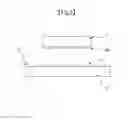
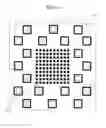
FIG. 5 is a plan view of a lower semiconductor chip 61 in a first modification of the embodiment according to the present invention. The lower semiconductor chip 61 is different from the lower semiconductor chip 6 shown in FIG. 2 in the pattern of dams 121. In the first modification, the external electrodes 9 located along the four sides of the lower semiconductor chip 61 are grouped, and the groups of external electrodes 9 are each enclosed by one dam 121. The dams 121 do not extend between adjacent external electrodes 9. The dams 121 provided in such a pattern are separated from each other at positions in the vicinity of four corners of the lower semiconductor chip 61, and gaps 13 through which the underfill resin 4 flows to an external peripheral area of the lower semiconductor chip 6 are provided at these positions. This structure can also achieve the object of the present invention.
FIG. 6 is a plan view of a lower semiconductor chip 62 in a second modification of the embodiment according to the present invention. The lower semiconductor chip 62 is different from the lower semiconductor chip 6 shown in
FIG. 2 in the pattern of dams 122. In the second modification, the external electrodes 9 located along the four sides of the lower semiconductor chip 62 are partially missing and thus gaps 132 are provided. The groups of external electrodes 9 separated from each other by the gaps 132 are enclosed by the dams 122 of different shapes from each other. The gaps 132 thus provided are large. Therefore, a larger amount of underfill resin 4 is allowed to flow to an external peripheral area of the lower semiconductor chip 62 than in the above embodiment and modification. This prevents the underfill resin 4 from flowing onto the external electrodes 9.
FIG. 7 is a plan view of a lower semiconductor chip 63 in a third modification of the embodiment according to the present invention. The lower semiconductor chip 63 is different from the lower semiconductor chip 6 shown in FIG. 2 in the pattern of the external electrodes 9 and the pattern of dams 123. In the third modification, the external electrodes 9 are located in two lines in a staggered manner along each side, and each external electrode is enclosed by one dam 123. This structure provides many gaps 133 extending to an external peripheral area of the lower semiconductor chip 63. Therefore, a larger amount of underfill resin 4 is allowed to flow to the external peripheral area of the lower semiconductor chip 63 than in the above embodiment and modifications. This prevents the underfill resin 4 from flowing onto the external electrodes 9.
So far, an embodiment according to the present invention and various modifications thereof have been described. The present invention is not limited to the above-described embodiment or modifications, and may be carried out in any of various modifications without departing from the gist of the present invention. For example, the dams are formed of solder at the same time as the solder bumps in the above description, but may be formed of a resin sheet of polyimide or epoxy instead of solder. The patterns of the external electrodes and the internal electrodes are variable in any of various manners.
The embodiment of the present invention and various modifications thereof provide any of the following effects.
-
- (1) The present invention provides a semiconductor device of a CoC connection which does not inhibit electrical contact between the external electrodes and the bonding wires and is not prevented from being reduced in size or from being mass-produced, and a method for producing such a semiconductor device.
- (2) In the case where solder is used to form dams in the present invention, the solder bumps on the internal electrodes and the dams can be formed at the same time. This simplifies the production process.
- (3) In the case where solder is used to form dams and the dams are provided in certain patterns in the present invention, the adhesiveness between the dams and the underlying layer is improved, which prevents the dams from being delaminated off.
Claims
What is claimed is:1. A semiconductor device, comprising:
a rectangular lower semiconductor element;
a plurality of external electrodes located in a pattern on the lower semiconductor element along sides thereof;
a plurality of internal electrodes electrically connected to the plurality of external electrodes via a plurality of line patterns respectively and located on the lower semiconductor element in a pattern;
dams provided in such a pattern that each of the dams encloses one or at least two external electrodes among the plurality of external electrodes;
an upper semiconductor element mounted on the lower semiconductor element such that a plurality of terminals on the upper semiconductor element are electrically connected to the plurality of internal electrodes respectively; and
a resin potted to flow to a space between the lower semiconductor element and the upper semiconductor element.
2. A semiconductor device according to claim 1, wherein the dams are formed of solder and are formed at the same time as solder bumps formed on the internal electrodes.
3. A semiconductor device according to claim 2, wherein:
an insulating film is provided on a surface of the lower semiconductor element;
the plurality of line patterns are provided on the insulating film; and
an insulating thin film having openings positionally corresponding to the plurality of internal electrodes and the plurality of external electrodes is provided on the line patterns.
4. A semiconductor device according to claim 1, wherein the dams have a gap therebetween, the gap extending from an area where the resin is potted to an external peripheral area of the lower semiconductor element.
5. A semiconductor device according to claim 1, wherein at least one of the dams encloses at least two external electrodes among the plurality of external electrodes and extends between the at least two external electrodes.
6. A method for producing a semiconductor device, comprising the steps of:
forming, on a rectangular lower semiconductor element, a plurality of external electrodes located in a pattern along sides of the lower semiconductor element, a plurality of internal electrodes located in a pattern, and line patterns for electrically connecting the plurality of external electrodes and the plurality of internal electrodes to each other respectively;
forming dams such that each of the dams encloses one or at least two external electrodes among the plurality of external electrodes;
mounting an upper semiconductor element on the lower semiconductor element such that a plurality of terminals on the upper semiconductor element are electrically connected to the plurality of internal electrodes respectively; and
potting a resin such that the resin flows to a space between the lower semiconductor element and the upper semiconductor element.
7. A method for producing a semiconductor device according to claim 6, wherein the dams are formed of solder and are formed at the same time as solder bumps formed on the internal electrodes.
8. A method for producing a semiconductor device according to claim 7, wherein:
an insulating film is formed on a surface of the lower semiconductor element;
the plurality of line patterns are formed on the insulating film; and
an insulating thin film having openings positionally corresponding to the plurality of internal electrodes and the plurality of external electrodes is formed on the line patterns.
9. A method for producing a semiconductor device according to claim 6, wherein the dams are formed to have a gap therebetween, the gap extending from an area where the resin is to be potted to an external peripheral area of the lower semiconductor element.
10. A method for producing a semiconductor device according to claim 6, wherein the dams are formed such that at least one of the dams encloses at least two external electrodes among the plurality of external electrodes and extends between the at least two external electrodes.
Images & Drawings included:


Sources:
- United States Patent and Trademark Office - verify current appl. status at the USPTO↗
Similar patent applications:
- » 20050221515
Method for producing semiconductor light emitting device, method for producing semiconductor device, method for producing device, method for growing nitride type III-V group compound semiconductor layer, method for growing semiconductor layer, and method for growing layer - » 20060172513
METHOD FOR PRODUCING SEMICONDUCTOR LIGHT EMITTING DEVICE, METHOD FOR PRODUCING SEMICONDUCTOR DEVICE, METHOD FOR PRODUCING DEVICE, METHOD FOR GROWING NITRIDE TYPE III-V GROUP COMPOUND SEMICONDUCTOR LAYER, METHOD FOR GROWING SEMICONDUCTOR LAYER, AND METHOD FOR GROWING LAYER - » 20060286695
METHOD FOR PRODUCING SEMICONDUCTOR LIGHT EMITTING DEVICE, METHOD FOR PRODUCING SEMICONDUCTOR DEVICE, METHOD FOR PRODUCING DEVICE, METHOD FOR GROWING NITRIDE TYPE III-V GROUP COMPOUND SEMICONDUCTOR LAYER, METHOD FOR GROWING SEMICONDUCTOR LAYER, AND METHOD FOR GROWING LAYER - » 20100317136
METHOD FOR PRODUCING SEMICONDUCTOR LIGHT EMITTING DEVICE, METHOD FOR PRODUCING SEMICONDUCTOR DEVICE, METHOD FOR PRODUCING DEVICE, METHOD FOR GROWING NITRIDE TYPE III-V GROUP COMPOUND SEMICONDUCTOR LAYER, METHOD FOR GROWING SEMICONDUCTOR LAYER, AND METHOD FOR GROWING LAYER - » 20050227458
Method for producing structured substrate, structured substrate, method for producing semiconductor light emitting device, semiconductor light emitting device, method for producing semiconductor device, semiconductor device, method for producing device, and device - » 20100019273
Method for producing structured substrate, structured substrate, method for producing semiconductor light emitting device, semiconductor light emitting device, method for producing semiconductor device, semiconductor device, method for producing device, and device - » 10396323
Semiconductor device producing method and semiconductor device producing apparatus including forming an oxide layer and changing the impedance or potential to form an oxynitride - » 20050236626
Semiconductor device, producing method of semiconductor substrate, and producing method of semiconductor device - » 9834923
Semiconductor device producing method and semiconductor device - » 20110298100
SEMICONDUCTOR DEVICE PRODUCING METHOD AND SEMICONDUCTOR DEVICE
Recent applications in this class:
- » 20250259905 2025-08-14
UNDERFILL VACUUM PROCESS - » 20250218887 2025-07-03
SEMICONDUCTOR DEVICE AND MANUFACTURING METHOD OF SEMICONDUCTOR DEVICE - » 20250174508 2025-05-29
SEMICONDUCTOR DEVICE PACKAGE - » 20250149396 2025-05-08
PACKAGE STRUCTURE - » 20250118611 2025-04-10
ELECTRONIC PACKAGE ASSEMBLY AND A METHOD FOR FORMING THE SAME - » 20250096058 2025-03-20
STAIR-STEP CONFIGURATION FOR A SEMICONDUCTOR DIE OF AN INTEGRATED CIRCUIT - » 20250087545 2025-03-13
Semiconductor Device and Method of Forming FOWLP with Pre-Molded Embedded Discrete Electrical Component - » 20240429119 2024-12-26
SEMICONDUCTOR APPARATUS - » 20240421019 2024-12-19
ELECTRONIC PACKAGE WITH REDISTRIBUTION LAYER PLATE FORMED VIA TEMPORARY PLUG - » 20240395648 2024-11-28
SEMICONDUCTOR DEVICE
Recent applications for this Assignee:
- » 20180342443 2018-11-29
Semiconductor package and a method for manufacturing a semiconductor device - » 20170316998 2017-11-02
Manufacturing method of semiconductor package including laser processing - » 20170316996 2017-11-02
Semiconductor package and manufacturing method of semiconductor package - » 20170301599 2017-10-19
Semiconductor device - » 20170170123 2017-06-15
Semiconductor package and its manufacturing method - » 20150243576 2015-08-27
SEMICONDUCTOR DEVICE - » 20140159215 2014-06-12
Semiconductor device and method of manufacturing the same - » 20140104953 2014-04-17
Semiconductor storage device and method for producing the same - » 20120074594 2012-03-29
Semiconductor device and manufacturing method thereof - » 20110309503 2011-12-22
Semiconductor device and manufacturing method thereof