Semiconductor package and fabrication method thereof
US20140353850A1
2014-12-04
13/971,189
2013-08-20
✅ Patent granted
US 9,502,377 B2
2016-11-22
-
-
John C Ingham | Ismail Muse
Mintz Levin Cohn Ferris Glovsky and Popeo, P.C. | Peter F. Corless | Steven M. Jensen
2033-08-20
Abstract:
A semiconductor package is disclosed, which includes: a circuit board; a carrier disposed on the circuit board; an RF chip disposed on the carrier; a plurality of high level bonding wires electrically connecting electrode pads of the RF chip and the circuit board; and an encapsulant formed on the circuit board for encapsulating the carrier, the high level bonding wires and the RF chip. The present invention positions the RF chip at a high level so as to facilitate element arrangement and high frequency wiring on the circuit board, thereby achieving a highly integrated wireless SiP (System in Package) module.
Inventors:
- Chao-Ya Yang 2 🇹🇼 Taichung Hsien, Taiwan
- Chih-Ming Cheng 2 🇹🇼 Taichung Hsien, Taiwan
- Chia-Yang Chen 2 🇹🇼 Taichung Hsien, Taiwan
- Chih-Hsien Chiu 1 🇹🇼 Taichung Hsien, Taiwan
- Tsung-Hsien Tsai 1 🇹🇼 Taichung Hsien, Taiwan
- Yude Chu 1 🇹🇼 Taichung Hsien, Taiwan
Assignee:
- Siliconware Precision Industries Co., Ltd. 673 🇹🇼 Taichung, Taiwan
Applicant:
Interested in similar patents?
Get notified when new applications in this technology area are published.
Classification:
H01L21/56 » CPC further
Processes or apparatus adapted for the manufacture or treatment of semiconductor or solid state devices or of parts thereof; Manufacture or treatment of semiconductor devices or of parts thereof the devices having at least one potential-jump barrier or surface barrier, e.g. PN junction, depletion layer or carrier concentration layer; Assembly of semiconductor devices using processes or apparatus not provided for in a single one of the subgroups - , e.g. sealing of a cap to a base of a container Encapsulations, e.g. encapsulation layers, coatings
H01L23/28 » CPC further
Details of semiconductor or other solid state devices Encapsulations, e.g. encapsulating layers, coatings, e.g. for protection
H01L23/12 » CPC further
Details of semiconductor or other solid state devices Mountings, e.g. non-detachable insulating substrates
H01L24/85 » CPC main
Arrangements for connecting or disconnecting semiconductor or solid-state bodies; Methods or apparatus related thereto; Methods for connecting semiconductor or other solid state bodies using means for bonding being attached to, or being formed on, the surface to be connected using a wire connector
H01L23/52 » CPC main
Details of semiconductor or other solid state devices Arrangements for conducting electric current within the device in operation from one component to another, i.e. interconnections, e.g. wires, lead frames
H01L23/00 IPC
Details of semiconductor or other solid state devices
H01L24/73 » CPC further
Arrangements for connecting or disconnecting semiconductor or solid-state bodies; Methods or apparatus related thereto Means for bonding being of different types provided for in two or more of groups , , , , , , ,
H01L23/4334 » CPC further
Details of semiconductor or other solid state devices; Arrangements for cooling, heating, ventilating or temperature compensation ; Temperature sensing arrangements; Fillings or auxiliary members in containers or encapsulations selected or arranged to facilitate heating or cooling; Auxiliary members in containers characterised by their shape, e.g. pistons Auxiliary members in encapsulations
H01L24/32 » CPC further
Arrangements for connecting or disconnecting semiconductor or solid-state bodies; Methods or apparatus related thereto; Means for bonding being attached to, or being formed on, the surface to be connected, e.g. chip-to-package, die-attach, "first-level" interconnects; Manufacturing methods related thereto; Layer connectors, e.g. plate connectors, solder or adhesive layers; Manufacturing methods related thereto; Structure, shape, material or disposition of the layer connectors after the connecting process of an individual layer connector
H01L23/3121 » CPC further
Details of semiconductor or other solid state devices; Encapsulations, e.g. encapsulating layers, coatings, e.g. for protection characterised by the arrangement or shape the device being completely enclosed a substrate forming part of the encapsulation
H01L23/66 » CPC further
Details of semiconductor or other solid state devices; Structural electrical arrangements for semiconductor devices not otherwise provided for, e.g. in combination with batteries; Impedance arrangements High-frequency adaptations
H01L2224/04042 » CPC further
Indexing scheme for arrangements for connecting or disconnecting semiconductor or solid-state bodies and methods related thereto as covered by; Means for bonding being attached to, or being formed on, the surface to be connected, e.g. chip-to-package, die-attach, "first-level" interconnects; Manufacturing methods related thereto; Bonding areas; Manufacturing methods related thereto; Structure, shape, material or disposition of the bonding areas prior to the connecting process Bonding areas specifically adapted for wire connectors, e.g. wirebond pads
H01L2224/73265 » CPC further
Indexing scheme for arrangements for connecting or disconnecting semiconductor or solid-state bodies and methods related thereto as covered by; Means for bonding being of different types provided for in two or more of groups; Location after the connecting process on different surfaces Layer and wire connectors
H01L2224/92247 » CPC further
Indexing scheme for arrangements for connecting or disconnecting semiconductor or solid-state bodies and methods related thereto as covered by; Methods for connecting semiconductor or solid state bodies including different methods provided for in two or more of groups - ; Specific sequence of method steps; Connecting different surfaces of the semiconductor or solid-state body with connectors of different types; Sequential connecting processes the first connecting process involving a layer connector the second connecting process involving a wire connector
H01L2225/0651 » CPC further
Details relating to assemblies covered by the group but not provided for in its subgroups; All the devices being of a type provided for in the same subgroup of groups - the devices not having separate containers the devices being of a type provided for in group; Stacked arrangements of devices Wire or wire-like electrical connections from device to substrate
H01L2225/06575 » CPC further
Details relating to assemblies covered by the group but not provided for in its subgroups; All the devices being of a type provided for in the same subgroup of groups - the devices not having separate containers the devices being of a type provided for in group; Stacked arrangements of devices Auxiliary carrier between devices, the carrier having no electrical connection structure
H01L2924/00014 » CPC further
Indexing scheme for arrangements or methods for connecting or disconnecting semiconductor or solid-state bodies as covered by; Technical content checked by a classifier the subject-matter covered by the group, the symbol of which is combined with the symbol of this group, being disclosed without further technical details
H01L2924/181 » CPC further
Indexing scheme for arrangements or methods for connecting or disconnecting semiconductor or solid-state bodies as covered by; Details of package parts other than the semiconductor or other solid state devices to be connected Encapsulation
H01L2924/19041 » CPC further
Indexing scheme for arrangements or methods for connecting or disconnecting semiconductor or solid-state bodies as covered by; Details of hybrid assemblies other than the semiconductor or other solid state devices to be connected; Structure; Component type being a capacitor
H01L2924/19042 » CPC further
Indexing scheme for arrangements or methods for connecting or disconnecting semiconductor or solid-state bodies as covered by; Details of hybrid assemblies other than the semiconductor or other solid state devices to be connected; Structure; Component type being an inductor
H01L2924/19043 » CPC further
Indexing scheme for arrangements or methods for connecting or disconnecting semiconductor or solid-state bodies as covered by; Details of hybrid assemblies other than the semiconductor or other solid state devices to be connected; Structure; Component type being a resistor
H01L2924/19103 » CPC further
Indexing scheme for arrangements or methods for connecting or disconnecting semiconductor or solid-state bodies as covered by; Details of hybrid assemblies other than the semiconductor or other solid state devices to be connected; Disposition of discrete passive components in a stacked assembly with the semiconductor or solid state device interposed between the semiconductor or solid-state device and the die mounting substrate, i.e. chip-on-passive
H01L2924/19104 » CPC further
Indexing scheme for arrangements or methods for connecting or disconnecting semiconductor or solid-state bodies as covered by; Details of hybrid assemblies other than the semiconductor or other solid state devices to be connected; Disposition of discrete passive components in a stacked assembly with the semiconductor or solid state device on the semiconductor or solid-state device, i.e. passive-on-chip
H01L23/552 » CPC further
Details of semiconductor or other solid state devices Protection against radiation, e.g. light or electromagnetic waves
H01L23/48 IPC
Details of semiconductor or other solid state devices Arrangements for conducting electric current to or from the solid state body in operation, e.g. leads, terminal arrangements ; Selection of materials therefor
H01L29/40 IPC
Semiconductor devices adapted for rectifying, amplifying, oscillating or switching, or capacitors or resistors with at least one potential-jump barrier or surface barrier, e.g. PN junction depletion layer or carrier concentration layer; Details of semiconductor bodies or of electrodes thereof; Multistep manufacturing processes therefor Electrodes ; Multistep manufacturing processes therefor
H01L23/433 IPC
Details of semiconductor or other solid state devices; Arrangements for cooling, heating, ventilating or temperature compensation ; Temperature sensing arrangements; Fillings or auxiliary members in containers or encapsulations selected or arranged to facilitate heating or cooling Auxiliary members in containers characterised by their shape, e.g. pistons
H01L25/065 IPC
Assemblies consisting of a plurality of individual semiconductor or other solid state devices ; Multistep manufacturing processes thereof all the devices being of a type provided for in the same subgroup of groups - , e.g. assemblies of rectifier diodes the devices not having separate containers the devices being of a type provided for in group
H01L23/31 IPC
Details of semiconductor or other solid state devices; Encapsulations, e.g. encapsulating layers, coatings, e.g. for protection characterised by the arrangement or shape
H01L24/48 » CPC further
Arrangements for connecting or disconnecting semiconductor or solid-state bodies; Methods or apparatus related thereto; Means for bonding being attached to, or being formed on, the surface to be connected, e.g. chip-to-package, die-attach, "first-level" interconnects; Manufacturing methods related thereto; Wire connectors; Manufacturing methods related thereto; Structure, shape, material or disposition of the wire connectors after the connecting process of an individual wire connector
H01L2224/83191 » CPC further
Indexing scheme for arrangements for connecting or disconnecting semiconductor or solid-state bodies and methods related thereto as covered by; Methods for connecting semiconductor or other solid state bodies using means for bonding being attached to, or being formed on, the surface to be connected using a layer connector; Arrangement of the layer connectors prior to mounting wherein the layer connectors are disposed only on the semiconductor or solid-state body
H01L2924/19105 » CPC further
Indexing scheme for arrangements or methods for connecting or disconnecting semiconductor or solid-state bodies as covered by; Details of hybrid assemblies other than the semiconductor or other solid state devices to be connected; Disposition of discrete passive components in a side-by-side arrangement on a common die mounting substrate
H01L25/0657 » CPC further
Assemblies consisting of a plurality of individual semiconductor or other solid state devices ; Multistep manufacturing processes thereof all the devices being of a type provided for in the same subgroup of groups - , e.g. assemblies of rectifier diodes the devices not having separate containers the devices being of a type provided for in group Stacked arrangements of devices
H01L2224/8592 » CPC further
Indexing scheme for arrangements for connecting or disconnecting semiconductor or solid-state bodies and methods related thereto as covered by; Methods for connecting semiconductor or other solid state bodies using means for bonding being attached to, or being formed on, the surface to be connected using a wire connector; Post-treatment of the connector or wire bonding area Applying permanent coating, e.g. protective coating
Description
BACKGROUND OF THE INVENTION
1. Field of the Invention
The present invention relates to semiconductor packages and fabrication methods thereof and more particularly, to a semiconductor package and a fabrication method thereof for improving the product reliability.
2. Description of Related Art
With the rapid development of electronic industries, electronic products are developed towards miniaturization, light weight and high speed processing. Radio frequency (RF) chips are required in a lot of electronic products. For the purpose of miniaturization or high speed processing, RF chips are usually integrated with digital integrated circuits (ICs), digital signal processors (DSPs) or baseband (BB) chips.
Currently, there are various types of chip packages. To achieve a small surface bonding area, a plurality of chips are usually disposed on a substrate in a stack manner and electrically connected to the substrate through wire bonding. To facilitate the wire bonding, the chips are disposed with their active surfaces facing upward. A dummy chip or a paste adhesive or film is disposed between two adjacent chips, thus allowing bonding wires to have sufficient wire loops.
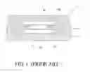
FIG. 1 is a schematic cross-sectional view of a conventional semiconductor package 1. Referring to FIG. 1, the semiconductor package 1 has a circuit board 10, an RF chip 12 disposed on the circuit board 10, a dummy chip 11 disposed on the RF chip 12, a semiconductor chip 14 disposed on the dummy chip 11, a plurality of first bonding wires 140 electrically connecting the semiconductor chip 14 and the circuit board 10, a plurality of second bonding wires 13 electrically connecting the RF chip 12 and the circuit board 10, and an encapsulant 16 encapsulating the dummy chip 11, the semiconductor chip 14, the first bonding wires 140, the RF chip 12 and the second bonding wires 13. Since a gap is provided between the semiconductor chip 14 and the RF chip 12 by the dummy chip 11, the second bonding wires 13 can be formed with a sufficient wire loop.
However, RF circuits of the RF chip 12 form a sensitive area easily affected by such as interferences and thermal factors, especially when the RF chip 12 is a high frequency chip or a wireless RF chip. As such, the flexibility of wiring and element arrangement is reduced and it becomes quite difficult to achieve a highly integrated wireless system in package (SiP) module.
Further, signals from the RF chip 12 and the semiconductor chip 14 arranged in a stack manner may interfere with each other and generate noises, especially when the RF chip 12 is a high frequency chip or a wireless RF chip, thereby seriously affecting operation of the semiconductor chip 14.
Therefore, there is a need to provide a semiconductor package and a fabrication method thereof so as to overcome the above-described drawbacks.
SUMMARY OF THE INVENTION
In view of the above-described drawbacks, the present invention provides a semiconductor package, which comprises: a circuit board; a carrier disposed on the circuit board; an RF chip disposed on the carrier, wherein the RF chip has an active surface with a plurality of electrode pads and an inactive surface opposite to the active surface, and the RF chip is disposed on the carrier via the inactive surface thereof; a plurality of high level bonding wires electrically connecting the electrode pads of the RF chip and the circuit board; and an encapsulant formed on the circuit board for encapsulating the carrier, the high level bonding wires and the RF chip.
The present invention further provides a fabrication method of a semiconductor package, which comprises the steps of: providing a circuit board having a carrier thereon; disposing an RF chip on the carrier, wherein the RF chip has an active surface with a plurality of electrode pads and an inactive surface opposite to the active surface, and the RF chip is disposed on the carrier via the inactive surface thereof; forming a plurality of high level bonding wires electrically connecting the electrode pads of the RF chip and the circuit board; and forming an encapsulant on the circuit board for encapsulating the carrier, the high level bonding wires and the RF chip.
In the above-described package and method, the carrier can be a functional chip, a dummy chip, a heat sink or an insulator.
In the above-described package and method, the RF chip can be greater in width than the carrier so as to form a receiving space between the RF chip and the circuit board. At least a semiconductor element can be disposed on the circuit board in a manner that the semiconductor element is received in the receiving space or located at a periphery of the carrier.
In the above-described package and method, the RF chip can be attached to the carrier through a bonding layer.
In the above-described package and method, a plurality of low level bonding wires can further be formed to connect the carrier and the circuit board, and the RF chip can be attached to the carrier through a bonding layer that partially encapsulates the low level bonding wires. In an embodiment, the low level bonding wires electrically connect the carrier and the circuit board. In another embodiment, the RF chip has a grounding layer formed on the inactive surface thereof, and the low level bonding wires are in contact with the grounding layer so as to ground the carrier to the circuit board.
According to the present invention, the RF chip is positioned at a high level and spaced from the circuit board to facilitate element arrangement and high frequency wiring on the circuit board, thus achieving a highly integrated wireless SiP (System in Package) module.
BRIEF DESCRIPTION OF DRAWINGS
FIG. 1 is a schematic cross-sectional view of a conventional semiconductor package; and
FIGS. 2A to 2D are schematic cross-sectional views showing a fabrication method of a semiconductor package according to the present invention, wherein FIG. 2C′ shows an embodiment of FIG. 2C, and FIGS. 2D′ and 2D″ show other embodiments of FIG. 2D.
DETAILED DESCRIPTION OF PREFERRED EMBODIMENTS
The following illustrative embodiments are provided to illustrate the disclosure of the present invention, these and other advantages and effects can be apparent to those in the art after reading this specification.
It should be noted that all the drawings are not intended to limit the present invention. Various modifications and variations can be made without departing from the spirit of the present invention. Further, terms such as “first”, “on”, “high level”, “low level”, “a” etc. are merely for illustrative purposes and should not be construed to limit the scope of the present invention.
FIGS. 2A to 2D are schematic cross-sectional views showing a fabrication method of a semiconductor package 2 according to the present invention.
Referring to FIG. 2A, a circuit board 20 having a carrier 21 thereon is provided. A plurality of semiconductor elements 24 are disposed on the circuit board 20.
In the present embodiment, the circuit board 20 has a plurality of first bonding pads 201 and a plurality of second bonding pads 202. The carrier 21 is attached to the circuit board 20 through an adhesive layer 200.
The carrier 21 can be a functional chip, a dummy chip, a heat sink or an insulator.
The semiconductor elements 24 can be resistors, capacitors or inductors and are located around a periphery of the carrier 21.
Referring to FIG. 2B, a plurality of low level bonding wires 210 are formed to electrically connect the carrier 21 and the first bonding pads 201 of the circuit board 20.
Referring to FIG. 2C, an RF chip 22 is disposed on the carrier 21. The RF chip 22 has an active surface 22a with a plurality of electrode pads 220 and an inactive surface 22b opposite to the active surface 22a. The RF chip 22 is disposed on the carrier 21 via the inactive surface 22b thereof.
Then, a plurality of high level bonding wires 23 are formed to electrically connect the electrode pads 220 of the RF chip 22 and the second bonding pads 202 of the circuit board 20.
In the present embodiment, the RF chip 22 is a high frequency chip or a wireless RF chip. The width W of the RF chip 22 is greater than the width d of the carrier 21. As such, a receiving space S is formed between the RF chip 22 and the circuit board 20 and the semiconductor elements 24 are received in the receiving space S. The receiving space S has a height of at least 0.2 mm.
Further, the RF chip 22 is attached to the carrier 21 through a bonding layer 25. By using a film over wire (FOW) technique the low level bonding wires 210 are partially encapsulated by the bonding layer 25. As such, the low level bonding wires 210 are prevented from crossing or coming into contact with the RF chip 22, thus preventing short circuits and facilitating wire bonding. In addition, such a structure meets the miniaturization requirement of semiconductor packages.
Referring to FIG. 2C′, the bonding layer 25 is formed on the inactive surface 22b of the RF chip 22 first and then the RF chip 22 is attached to the carrier 21 through the bonding layer 25. In an alternative embodiment, the bonding layer 25 is formed on the carrier 21 and then the RF chip 22 is attached to the bonding layer 25 of the carrier 21 via the inactive surface 22b thereof.
Referring to FIG. 2D, an encapsulant 26 is formed on the circuit board 20 for encapsulating the carrier 21, the RF chip 22, the low level bonding wires 210 and the high level bonding wires 23.
In the present embodiment, the encapsulant 26 is made of a molding compound and formed through a molding process. In other embodiments, the encapsulant 26 can be made of a thin film and formed through lamination, or made of an adhesive and formed through printing.
According to the present invention, the RF chip 22 is positioned at a suitable high level so as to form the receiving space S between the RF chip 22 and the circuit board 20, thereby facilitating arrangement of elements, such as the semiconductor element 24, and high frequency wiring on the circuit board 20 and hence increasing the flexibility of wiring and element arrangement. Therefore, a highly integrated wireless SiP module can be achieved.
Further, by positioning the RF chip 22 at a suitable high level, the present invention prevents interference of the RF chip 22 with the semiconductor element 24 or circuits of the circuit board 20.
In another embodiment, referring to FIG. 2D′, a grounding layer 27 is formed on the inactive surface 22b of the RF chip 22, and the low level bonding wires 210′ are in contact with the grounding layer 27 so as to ground the carrier 21 to the first bonding pads 201′. As such, the carrier 21 does not have an electrical function.
In another embodiment, referring to FIG. 2D″, the carrier 21 is grounded to the first bonding pads 201′ through a portion of the low level bonding wires 210′ and electrically connected to the first bonding pads 201 through another portion of the low level bonding wires 210. As such, the carrier 21 has an electrical function.
The present invention further provides a semiconductor package 2, 2′, 2″, which has: a circuit board 20; a carrier 21 disposed on the circuit board 20; an RF chip 22 disposed on the carrier 21, wherein the RF chip 22 has an active surface 22a with a plurality of electrode pads 220 and an inactive surface 22b opposite to the active surface 22a, and the RF chip 22 is disposed on the carrier 21 via the inactive surface 22b thereof; a plurality of high level bonding wires 23 electrically connecting the electrode pads 220 of the RF chip 22 and the circuit board 20; and an encapsulant 26 formed on the circuit board 20 for encapsulating the carrier 21, the high level bonding wires 23 and the RF chip 22.
The carrier 21 can be a functional chip, a dummy chip, a heat sink or an insulator.
The width W of the RF chip 22 can be greater than the width d of the carrier 21 so as to form a receiving space S between the RF chip 22 and the circuit board 20. Further, at least a semiconductor element 24 can be disposed on the circuit board 20 and received in the receiving space S or located a periphery of the carrier 21.
The RF chip 22 can be attached to the carrier 21 through a bonding layer 25, a plurality of low level bonding wires 210 can be formed to electrically connect the carrier 21 and the circuit board 20, and the low level bonding wires 210 can be partially encapsulated by the bonding layer 25.
In an embodiment, the RF chip 22 has a grounding layer 27 formed on the inactive surface 22b thereof, and the low level bonding wires 210′ are in contact with the grounding layer 27 so as to ground the carrier 21 to the circuit board 20. In an alternative embodiment, the carrier 21 can be grounded to the circuit board 20 through a portion of the low level bonding wires 210′ and electrically connected to the circuit board 20 through another portion of the low level bonding wires 210.
Therefore, the present invention positions the RF chip at a high level to facilitate element arrangement and high frequency wiring so as to achieve a highly integrated wireless SiP module.
The above-described descriptions of the detailed embodiments are only to illustrate the preferred implementation according to the present invention, and it is not to limit the scope of the present invention. Accordingly, all modifications and variations completed by those with ordinary skill in the art should fall within the scope of present invention defined by the appended claims.
Claims
1. A semiconductor package, comprising:
a circuit board;
a carrier disposed on the circuit board;
an RF chip disposed on the carrier, wherein the RF chip has an active surface with a plurality of electrode pads and an inactive surface opposite to the active surface, and the RF chip is disposed on the carrier via the inactive surface thereof, wherein a grounding layer is formed on the inactive surface of the RF chip and is free from being directly in contact with the carrier;
a plurality of high level bonding wires electrically connecting the electrode pads of the RF chip and the circuit board; and
an encapsulant formed on the circuit board for encapsulating the carrier, the high level bonding wires and the RF chip.
2. The package of claim 1, wherein the carrier is a functional chip, a dummy chip, a heat sink or an insulator.
3. The package of claim 1, wherein the RF chip is greater in width than the carrier so as to form a receiving space between the RF chip and the circuit board.
4. The package of claim 3, further comprising at least a semiconductor element disposed on the circuit board and received in the receiving space.
5. The package of claim 1, further comprising at least a semiconductor element disposed on the circuit board.
6. The package of claim 5, wherein the semiconductor element is located at a periphery of the carrier.
7. The package of claim 1, wherein the RF chip is attached to the carrier through a bonding layer.
8. The package of claim 1, further comprising a plurality of low level bonding wires connecting the carrier and the circuit board, and wherein the RF chip is attached to the carrier through a bonding layer.
9. The package of claim 8, wherein the low level bonding wires electrically connect the carrier and the circuit board.
10. The package of claim 9, wherein the bonding layer partially encapsulates the low level bonding wires.
11. The package of claim 8, wherein the low level bonding wires are in contact with the grounding layer so as to ground the carrier to the circuit board.
12. The package of claim 11, wherein the carrier is grounded to the circuit board through a portion of the low level bonding wires and electrically connected to the circuit board through another portion of the low level bonding wires.
13. The package of claim 10, wherein the low level bonding wires are in contact with the grounding layer so as to ground the carrier to the circuit board.
14. The package of claim 13, wherein the carrier is grounded to the circuit board through a portion of the low level bonding wires and electrically connected to the circuit board through another portion of the low level bonding wires.
15. A fabrication method of a semiconductor package, comprising the steps of:
providing a circuit board having a carrier thereon;
disposing an RF chip on the carrier, wherein the RF chip has an active surface with a plurality of electrode pads and an inactive surface opposite to the active surface, and the RF chip is disposed on the carrier via the inactive surface thereof, wherein a grounding layer is formed on the inactive surface of the RF chip and is free from being directly in contact with the carrier;
forming a plurality of high level bonding wires electrically connecting the electrode pads of the RF chip and the circuit board; and
forming an encapsulant on the circuit board for encapsulating the carrier, the high level bonding wires and the RF chip.
16. The method of claim 15, wherein the carrier is a functional chip, a dummy chip, a heat sink or an insulator.
17. The method of claim 15, wherein the RF chip is greater in width than the carrier so as to form a receiving space between the RF chip and the circuit board.
18. The method of claim 17, further comprising disposing at least a semiconductor element on the circuit board in a manner that the semiconductor element is received in the receiving space.
19. The method of claim 15, further comprising disposing at least a semiconductor element on the circuit board.
20. The method of claim 19, wherein the semiconductor element is located at a periphery of the carrier.
21. The method of claim 15, wherein the RF chip is attached to the carrier through a bonding layer.
22. The method of claim 15, further comprising forming a plurality of low level bonding wires connecting the carrier and the circuit board, and wherein the RF chip is attached to the carrier through a bonding layer.
23. The method of claim 22, wherein the low level bonding wires electrically connect the carrier and the circuit board.
24. The method of claim 23, wherein the bonding layer partially encapsulates the low level bonding wires.
25. The method of claim 22, wherein the low level bonding wires are in contact with the grounding layer so as to ground the carrier to the circuit board.
26. The method of claim 25, wherein the carrier is grounded to the circuit board through a portion of the low level bonding wires and electrically connected to the circuit board through another portion of the low level bonding wires.
Images & Drawings included:


Sources:
- United States Patent and Trademark Office - verify current appl. status at the USPTO↗
Similar patent applications:
- » 20090283903
Bump with multiple vias for semiconductor package and fabrication method thereof, and semiconductor package utilizing the same - » 20140264958
SEMICONDUCTOR PACKAGE, FABRICATION METHOD THEREOF AND MOLDING COMPOUND - » 15207186
Semiconductor package and fabricating method thereof - » 9709523
Semiconductor package and fabrication method thereof - » 10649847
Light sensitive semiconductor package and fabrication method thereof - » 15135539
Semiconductor package and fabrication method thereof - » 11933908
Semiconductor package and fabrication method thereof - » 10404173
Semiconductor package and fabrication method thereof - » 11734999
Semiconductor package and fabricating method thereof - » 14823689
Semiconductor package and fabricating method thereof
Recent applications in this class:
- » 20250167100 2025-05-22
PACKAGED ELECTRONIC DEVICE HAVING HIGH THERMAL DISSIPATION COMPRISING A PLURALITY OF POWER TRANSISTORS AND MANUFACTURING PROCESS THEROF - » 20250118653 2025-04-10
Stack of Horizontally Extending and Vertically Overlapping Features, Methods of Forming Circuitry Components, and Methods of Forming an Array of Memory Cells - » 20240332161 2024-10-03
SEMICONDUCTOR DEVICE - » 20240186234 2024-06-06
Stack of Horizontally Extending and Vertically Overlapping Features, Methods of Forming Circuitry Components, and Methods of Forming an Array of Memory Cells - » 20230369197 2023-11-16
OPTICAL ROUTING STRUCTURE ON BACKSIDE OF SUBSTRATE FOR PHOTONIC DEVICES - » 20230282567 2023-09-07
Power Semiconductor Module with Two Opposite Half-Bridges - » 20220352063 2022-11-03
Optical routing structure on backside of substrate for photonic devices - » 20220302015 2022-09-22
Stack of horizontally extending and vertically overlapping features, methods of forming circuitry components, and methods of forming an array of memory cells - » 20210296226 2021-09-23
Semiconductor device, method for manufacturing the same, and semiconductor module - » 20210193564 2021-06-24
Optical routing structure on backside of substrate for photonic devices
Recent applications for this Assignee:
- » 20250046771 2025-02-06
METHOD FOR FABRICATING ELECTRONIC PACKAGE - » 20250015054 2025-01-09
CARRYING SUBSTRATE, ELECTRONIC PACKAGE HAVING THE CARRYING SUBSTRATE, AND METHODS FOR MANUFACTURING THE SAME - » 20240379534 2024-11-14
ELECTRONIC PACKAGE, MANUFACTURING METHOD FOR THE SAME, AND ELECTRONIC STRUCTURE - » 20240321798 2024-09-26
Electronic package and carrier thereof and method for manufacturing the same - » 20240321784 2024-09-26
Electronic package including lead frame having multiple conductive posts - » 20240321591 2024-09-26
METHOD FOR FABRICATING ELECTRONIC PACKAGE - » 20240290701 2024-08-29
ELECTRONIC PACKAGE AND MANUFACTURING METHOD THEREOF - » 20240290675 2024-08-29
Electronic package and manufacturing method thereof - » 20240290674 2024-08-29
ELECTRONIC PACKAGE AND MANUFACTURING METHOD THEREOF - » 20240282674 2024-08-22
ELECTRONIC PACKAGE AND METHOD OF FABRICATING THE SAME