Graphene transistor
US20140361250A1
2014-12-11
14/345,093
2012-09-26
✅ Patent granted
US 9,171,907 B2
2015-10-27
WO; PCT/US2012/057249; 20120926
WO; WO2013/049144; 20130404
Jarrett Stark | Shahed Ahmed
Bryan W. Bockhop | Bockhop & Associates, LLC
2032-09-26
Abstract:
A transistor includes a silicon carbide crystal (110) having a silicon terminated face (112). A semiconducting-type graphene layer (120) is bonded to the silicon terminated face (112). A first semimetallic-type graphene layer (122) is contiguous with a first portion of the semiconducting-type graphene layer (120). A second semimetallic-type graphene layer (122) is contiguous with a second portion of the semiconducting-type graphene layer (120) that is spaced apart from the first portion. An insulator layer (132) is disposed on a portion of the semiconducting-type graphene layer (120). A gate conductive layer (134) disposed on the insulator layer (132) and spaced apart from the semiconducting-type graphene layer (120).
Assignee:
- Georgia Tech Research Corporation 1,721 🇺🇸 Atlanta, GA, United States
Applicant:
Interested in similar patents?
Get notified when new applications in this technology area are published.
Classification:
H01L29/1606 » CPC main
Semiconductor devices adapted for rectifying, amplifying, oscillating or switching, or capacitors or resistors with at least one potential-jump barrier or surface barrier, e.g. PN junction depletion layer or carrier concentration layer; Details of semiconductor bodies or of electrodes thereof; Multistep manufacturing processes therefor; Semiconductor bodies ; Multistep manufacturing processes therefor characterised by the materials of which they are formed including, apart from doping materials or other impurities, only elements of Group IV of the Periodic System Graphene
H01L21/02664 » CPC further
Processes or apparatus adapted for the manufacture or treatment of semiconductor or solid state devices or of parts thereof; Manufacture or treatment of semiconductor devices or of parts thereof; Forming layers; Forming inorganic semiconducting materials on a substrate; Special treatments Aftertreatments
H01L29/417 IPC
Semiconductor devices adapted for rectifying, amplifying, oscillating or switching, or capacitors or resistors with at least one potential-jump barrier or surface barrier, e.g. PN junction depletion layer or carrier concentration layer; Details of semiconductor bodies or of electrodes thereof; Multistep manufacturing processes therefor; Electrodes ; Multistep manufacturing processes therefor characterised by their shape, relative sizes or dispositions carrying the current to be rectified, amplified or switched
H01L29/1608 » CPC further
Semiconductor devices adapted for rectifying, amplifying, oscillating or switching, or capacitors or resistors with at least one potential-jump barrier or surface barrier, e.g. PN junction depletion layer or carrier concentration layer; Details of semiconductor bodies or of electrodes thereof; Multistep manufacturing processes therefor; Semiconductor bodies ; Multistep manufacturing processes therefor characterised by the materials of which they are formed including, apart from doping materials or other impurities, only elements of Group IV of the Periodic System Silicon carbide
H01L29/41758 » CPC further
Semiconductor devices adapted for rectifying, amplifying, oscillating or switching, or capacitors or resistors with at least one potential-jump barrier or surface barrier, e.g. PN junction depletion layer or carrier concentration layer; Details of semiconductor bodies or of electrodes thereof; Multistep manufacturing processes therefor; Electrodes ; Multistep manufacturing processes therefor characterised by their shape, relative sizes or dispositions carrying the current to be rectified, amplified or switched; Source or drain electrodes for field effect devices for lateral devices with structured layout for source or drain region, i.e. the source or drain region having cellular, interdigitated or ring structure or being curved or angular
H01L29/66477 » CPC further
Semiconductor devices adapted for rectifying, amplifying, oscillating or switching, or capacitors or resistors with at least one potential-jump barrier or surface barrier, e.g. PN junction depletion layer or carrier concentration layer; Details of semiconductor bodies or of electrodes thereof; Multistep manufacturing processes therefor; Types of semiconductor device ; Multistep manufacturing processes therefor; Multistep manufacturing processes of devices having semiconductor bodies comprising group 14 or group 13/15 materials the devices being controllable only by the electric current supplied or the electric potential applied, to an electrode which does not carry the current to be rectified, amplified or switched, e.g. three-terminal devices; Unipolar field-effect transistors with an insulated gate, i.e. MISFET
H01L29/16 IPC
Semiconductor devices adapted for rectifying, amplifying, oscillating or switching, or capacitors or resistors with at least one potential-jump barrier or surface barrier, e.g. PN junction depletion layer or carrier concentration layer; Details of semiconductor bodies or of electrodes thereof; Multistep manufacturing processes therefor; Semiconductor bodies ; Multistep manufacturing processes therefor characterised by the materials of which they are formed including, apart from doping materials or other impurities, only elements of Group IV of the Periodic System
H01L29/66 IPC
Semiconductor devices adapted for rectifying, amplifying, oscillating or switching, or capacitors or resistors with at least one potential-jump barrier or surface barrier, e.g. PN junction depletion layer or carrier concentration layer; Details of semiconductor bodies or of electrodes thereof; Multistep manufacturing processes therefor Types of semiconductor device ; Multistep manufacturing processes therefor
H01L21/02 IPC
Processes or apparatus adapted for the manufacture or treatment of semiconductor or solid state devices or of parts thereof Manufacture or treatment of semiconductor devices or of parts thereof
H01L29/165 » CPC further
Semiconductor devices adapted for rectifying, amplifying, oscillating or switching, or capacitors or resistors with at least one potential-jump barrier or surface barrier, e.g. PN junction depletion layer or carrier concentration layer; Details of semiconductor bodies or of electrodes thereof; Multistep manufacturing processes therefor; Semiconductor bodies ; Multistep manufacturing processes therefor characterised by the materials of which they are formed including, apart from doping materials or other impurities, only elements of Group IV of the Periodic System including two or more of the elements provided for in group , e.g. alloys in different semiconductor regions, e.g. heterojunctions
H01L29/78 » CPC further
Semiconductor devices adapted for rectifying, amplifying, oscillating or switching, or capacitors or resistors with at least one potential-jump barrier or surface barrier, e.g. PN junction depletion layer or carrier concentration layer; Details of semiconductor bodies or of electrodes thereof; Multistep manufacturing processes therefor; Types of semiconductor device ; Multistep manufacturing processes therefor controllable by only the electric current supplied, or only the electric potential applied, to an electrode which does not carry the current to be rectified, amplified or switched; Unipolar devices, e.g. field effect transistors; Field effect transistors with field effect produced by an insulated gate
H01L21/02612 » CPC further
Processes or apparatus adapted for the manufacture or treatment of semiconductor or solid state devices or of parts thereof; Manufacture or treatment of semiconductor devices or of parts thereof; Forming layers; Forming inorganic semiconducting materials on a substrate Formation types
H01L29/0657 » CPC further
Semiconductor devices adapted for rectifying, amplifying, oscillating or switching, or capacitors or resistors with at least one potential-jump barrier or surface barrier, e.g. PN junction depletion layer or carrier concentration layer; Details of semiconductor bodies or of electrodes thereof; Multistep manufacturing processes therefor; Semiconductor bodies ; Multistep manufacturing processes therefor characterised by their shape; characterised by the shapes, relative sizes, or dispositions of the semiconductor regions ; characterised by the concentration or distribution of impurities within semiconductor regions characterised by the shape of the body
H01L29/66431 » CPC further
Semiconductor devices adapted for rectifying, amplifying, oscillating or switching, or capacitors or resistors with at least one potential-jump barrier or surface barrier, e.g. PN junction depletion layer or carrier concentration layer; Details of semiconductor bodies or of electrodes thereof; Multistep manufacturing processes therefor; Types of semiconductor device ; Multistep manufacturing processes therefor; Multistep manufacturing processes of devices having semiconductor bodies comprising group 14 or group 13/15 materials the devices being controllable only by the electric current supplied or the electric potential applied, to an electrode which does not carry the current to be rectified, amplified or switched, e.g. three-terminal devices; Unipolar field-effect transistors with a heterojunction interface channel or gate, e.g. HFET, HIGFET, SISFET, HJFET, HEMT
H01L29/7781 » CPC further
Semiconductor devices adapted for rectifying, amplifying, oscillating or switching, or capacitors or resistors with at least one potential-jump barrier or surface barrier, e.g. PN junction depletion layer or carrier concentration layer; Details of semiconductor bodies or of electrodes thereof; Multistep manufacturing processes therefor; Types of semiconductor device ; Multistep manufacturing processes therefor controllable by only the electric current supplied, or only the electric potential applied, to an electrode which does not carry the current to be rectified, amplified or switched; Unipolar devices, e.g. field effect transistors; Field effect transistors with two-dimensional charge carrier gas channel, e.g. HEMT ; with two-dimensional charge-carrier layer formed at a heterojunction interface with inverted single heterostructure, i.e. with active layer formed on top of wide bandgap layer, e.g. IHEMT
H01L29/76 IPC
Semiconductor devices adapted for rectifying, amplifying, oscillating or switching, or capacitors or resistors with at least one potential-jump barrier or surface barrier, e.g. PN junction depletion layer or carrier concentration layer; Details of semiconductor bodies or of electrodes thereof; Multistep manufacturing processes therefor; Types of semiconductor device ; Multistep manufacturing processes therefor controllable by only the electric current supplied, or only the electric potential applied, to an electrode which does not carry the current to be rectified, amplified or switched Unipolar devices, e.g. field effect transistors
H01L29/778 IPC
Semiconductor devices adapted for rectifying, amplifying, oscillating or switching, or capacitors or resistors with at least one potential-jump barrier or surface barrier, e.g. PN junction depletion layer or carrier concentration layer; Details of semiconductor bodies or of electrodes thereof; Multistep manufacturing processes therefor; Types of semiconductor device ; Multistep manufacturing processes therefor controllable by only the electric current supplied, or only the electric potential applied, to an electrode which does not carry the current to be rectified, amplified or switched; Unipolar devices, e.g. field effect transistors; Field effect transistors with two-dimensional charge carrier gas channel, e.g. HEMT ; with two-dimensional charge-carrier layer formed at a heterojunction interface
H01L29/06 IPC
Semiconductor devices adapted for rectifying, amplifying, oscillating or switching, or capacitors or resistors with at least one potential-jump barrier or surface barrier, e.g. PN junction depletion layer or carrier concentration layer; Details of semiconductor bodies or of electrodes thereof; Multistep manufacturing processes therefor; Semiconductor bodies ; Multistep manufacturing processes therefor characterised by their shape; characterised by the shapes, relative sizes, or dispositions of the semiconductor regions ; characterised by the concentration or distribution of impurities within semiconductor regions
Description
CROSS-REFERENCE TO RELATED APPLICATION(S)
This application claims the benefit of U.S. Provisional Patent Application Ser. No. 61/539,664, filed Sep. 27, 2011, the entirety of which is hereby incorporated herein by reference.
This application claims the benefit of International Patent Application No. PCT/US12/57249, filed Sep. 26, 2012, the entirety of which is hereby incorporated herein by reference.
STATEMENT OF GOVERNMENT INTEREST
This invention was made with government support under agreement No. DMR-082382, awarded by the National Science Foundation. The government has certain rights in the invention.
BACKGROUND OF THE INVENTION
1. Field of the Invention
The present invention relates to graphitic devices and, more specifically, to a graphene transistor.
2. Description of the Related Art
Microelectronic circuits are fundamental to virtually all digital systems in existence. Current circuit technology employs semiconductor transistors that are coupled to each other with conductors, such as metal and polysilicon. Electrical current flowing through such conductors results in heat generation. A circuit density increases, heat generation becomes an increasingly significant problem.
One area currently being explored involves nano-scale carbon-based circuitry. For example, carbon nanotubes have the property of ballistic charge transport, in which when current flows through a nanotube almost no heat is generated. Unfortunately, because carbon nanotubes cannot currently be grown in a pattern corresponding to a desired practical scale circuit, use of carbon nanotube circuits are not currently seen as a viable solution.
Recently, graphene circuits have been proposed. Graphene is an allotrope of carbon that is only one atom thick. Graphene circuits employ a substantially flat graphene layer that has been patterned using conventional micro-electronic lithographic patterning techniques. The graphene can be patterned into channels with dimensions approximating the dimensions of carbon nanotubes, thereby achieving near-ballistic charge transport properties.
One difficulty currently experienced with graphene based electronics is that graphene behaves as a semimetal and not a semiconductor. As a result, most graphene transistors do not effectively function as switches due to large source to drain leakage currents. As a result, most attempts at making graphene transistors result in transistors that cannot be switched off. This problem has been approached by several different methods. In one method, very narrow graphene ribbons are produced which are often observed to have a band gap. In another method, attempts have been made to chemically functionalize graphene to give the functionalized regions of the graphene semiconductor properties. These approaches have not yet yielded graphene transistors that can be used in practical applications.
Therefore, there is a need for graphene-based transistors in which regions of the graphene have semiconducting properties. There is also a need for a method of making semiconducting graphene.
SUMMARY OF THE INVENTION
The disadvantages of the prior art are overcome by the present invention which, in one aspect, is a transistor that includes a silicon carbide crystal having a silicon terminated face. A semiconducting-type graphene layer is bonded to the silicon terminated face. A first semimetallic-type graphene layer is contiguous with a first portion of the semiconducting-type graphene layer. A second semimetallic-type graphene layer is contiguous with a second portion of the semiconducting-type graphene layer that is spaced apart from the first portion. An insulator layer is disposed on a portion of the semiconducting-type graphene layer. A gate conductive layer disposed on the insulator layer and spaced apart from the semiconducting-type graphene layer.
In another aspect, the invention is a method of making a transistor in which a semiconducting-type graphene layer is formed on a silicon terminated face of a silicon carbide crystal. At least one semimetallic-type graphene layer is formed adjacent to the silicon carbide crystal so that the semimetallic-type graphene layer is contiguous with the semiconducting-type graphene layer. An insulator layer is applied on a portion of the semiconducting layer. A conductor layer is applied to the insulator layer.
These and other aspects of the invention will become apparent from the following description of the preferred embodiments taken in conjunction with the following drawings. As would be obvious to one skilled in the art, many variations and modifications of the invention may be effected without departing from the spirit and scope of the novel concepts of the disclosure.
BRIEF DESCRIPTION OF THE FIGURES OF THE DRAWINGS
FIGS. 1A-1E are a schematic diagrams demonstrating a sidewall embodiment.
FIGS. 2A-2D are schematic diagrams demonstrating a flat embodiment.
FIGS. 3A-3E are schematic diagrams demonstrating a passivated layer embodiment.
DETAILED DESCRIPTION OF THE INVENTION
A preferred embodiment of the invention is now described in detail. Referring to the drawings, like numbers indicate like parts throughout the views. Unless otherwise specifically indicated in the disclosure that follows, the drawings are not necessarily drawn to scale. As used in the description herein and throughout the claims, the following terms take the meanings explicitly associated herein, unless the context clearly dictates otherwise: the meaning of “a,” “an,” and “the” includes plural reference, the meaning of “in” includes “in” and “on.”
Methods of making thin film graphene on silicon carbide crystals through annealing are shown in U.S. Pat. No. 7,015,142, and in U.S. Patent Publication No. US-2009-0226638-A1, both of which are incorporated herein by reference.
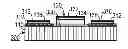
As shown in FIGS. 1A-1E, one embodiment of a transistor 100 is formed on a silicon terminated face 112 (e.g., the 0001 face) of a silicon carbide crystal 110. A mask 114 may be applied to the silicon terminated face 112, which is then subject to an etching process (e.g., oxygen plasma etching, chemical etching, ion beam etching, etc.) so as to form a raised portion 118 having opposing sidewalls 116. Because the sidewalls 116 are transverse to the silicon terminated face, they are not silicon terminated. As shown in FIG. 1C, the resulting crystal 110 is subjected to an annealing process (e.g., by heating it to a temperature of between 1000° C. and 2000° C. in a partial vacuum) that causes silicon atoms to evaporate from the crystal 110, leaving a layer 0-type graphene layer 120 (referred to as a “buffer layer”) on the silicon terminated face 112 and a layer of 1-type graphene layer 122 on the sidewalls 116. The layer 0-type graphene layer 120 is contiguous with the layer 1-type graphene layer 122 and the junction between the two layers is seamless. Because the layer 0-type graphene layer 120 is bonded directly to the silicon terminated face 112 of the crystal 110, it exhibits the properties of a semiconductor such that it exhibits a band gap of about 0.3 eV-0.5 EV. Because the layer 1-type graphene layer 122 on the sidewalls 116 is not bonded to a silicon terminated face, it exhibits semimetallic properties and can act as a conductor. The top-most layers of graphene (whether layer 0-type or layer 1-type) will be contiguous and join seamlessly.
As shown in FIG. 1D, a dielectric insulator layer 132 is deposited on a top portion of the layer 0-type graphene layer 120 and a first conductor layer (e.g., a metal layer) 134 is deposited on the dielectric insulator layer 132. Together, these two layers form a gate 130. A second conductor layer 136 is deposited on one of the layer 1-type graphene layers 122 to form a source contact and a third conductor layer 138 is deposited on one of the layer 1-type graphene layers 122 to form a drain contact. This structure can be modeled as a transistor 100, as shown in FIG. 1E.
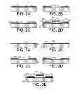
In another embodiment, as shown in FIGS. 2A-2D, at least two graphene layers are grown on the silicon terminated face 112 of a silicon carbide crystal 110 through a first annealing process in which silicon atoms are evaporated from the surface of the crystal 110. The graphene layers include a layer 0-type layer 212 that is bonded to the silicon terminated face 112 and at least one layer 1-type layer 222 that is bonded to the layer 0-type layer 212. As shown in FIG. 2B, an area 220 is etched into the two layers, thereby exposing a portion of the silicon terminated face 112 of the silicon carbide crystal 110. (In one example, an oxygen plasma etch is employed.) As shown in FIG. 2C, a second layer 0-type graphene layer 230 is then grown on the exposed portion of the silicon terminated face 112 through a second annealing process. This layer 0-type graphene layer 230 acts as a semiconductor, whereas the remaining layer 1-type graphene layers 222 have semimetallic conducting properties. A gate structure 130, as described above, is deposited on to the second layer 0-type graphene layer 230 and a source contact 136 and a drain contact 138 are deposited on to the layer 1-type graphene layers 222, as shown in FIG. 2D.
In yet another embodiment, as shown in FIGS. 3A-3E, a graphene buffer layer 312 is grown on a silicon terminated face 112 of a silicon carbide crystal 110. As shown in FIG. 3B, the surface 112 of the silicon carbide crystal 110 is passivated by subjecting it to a hydrogen gas environment, thereby forming a passivated silicon carbide surface 112. As a result, the bonds between the silicon carbide crystal 110 and the graphene layer 312 are broken and the graphene layer is now a layer 0*-type layer (which may be referred to as “passivated graphene”), which is quasi free standing and which acts as a semimetallic layer. In one experimental example, the hydrogen-rich environment included a one atmosphere partial pressure of hydrogen and the graphene layer 312 was heated to about 550° C. for about 75 minutes in the hydrogen-rich environment. As shown in FIG. 3C, an opening 328 is etched to expose a portion of the silicon terminated face 112. As shown in FIG. 3D, a second annealing results in a second layer 0-type graphene layer forming on the exposed portion of the silicon terminated face 112, which couples seamlessly to the layer 0*-type graphene layer 316. A gate structure 130, as described above, is deposited on to the layer 0-type graphene layer 330 and a source contact 136 and a drain contact 138 are deposited on to the layer 0*-type graphene layers 316, as shown in FIG. 3E. A portion of the layer 0*-type graphene layer 316 can be converted back to layer 0-type graphene by subjecting it to a hydrogen-poor environment (e.g., a partial vacuum) and heating it (e.g., to about 900° C.) for a predetermined amount of time.
The above embodiments may employ one of many known patterning processes to generate complex integrated circuits. When the sources and drains of the above disclosed transistors are subjected to a suitable bias voltage and when the gates are subjected to a gate voltage, the resulting field generated by the gate will cause current to flow through the semiconducting layer 0-type graphene subjected to the field. Thus, these transistors act as switches, thereby making them suitable for digital circuit applications.
The above described embodiments, while including the preferred embodiment and the best mode of the invention known to the inventor at the time of filing, are given as illustrative examples only. It will be readily appreciated that many deviations may be made from the specific embodiments disclosed in this specification without departing from the spirit and scope of the invention. Accordingly, the scope of the invention is to be determined by the claims below rather than being limited to the specifically described embodiments above.
Claims
What is claimed is:1. A transistor, comprising:
(a) a silicon carbide crystal having a silicon terminated face;
(b) a semiconducting-type graphene layer bonded to the silicon terminated face;
(c) a first semimetallic-type graphene layer contiguous with a first portion of the semiconducting-type graphene layer;
(d) a second semimetallic-type graphene layer contiguous with a second portion of the semiconducting-type graphene layer that is spaced apart from the first portion;
(e) an insulator layer disposed on a portion of the semiconducting-type graphene layer; and
(f) a gate conductive layer disposed on the insulator layer and spaced apart from the semiconducting-type graphene layer.
2. The transistor of claim 1, wherein the semiconducting-type graphene layer comprises a layer 0-type graphene.
3. The transistor of claim 1, wherein at least one of the first semimetallic-type graphene layer and the second semimetallic-type graphene layer comprises a layer 1-type graphene.
4. The transistor of claim 1, wherein at least one of the first semimetallic-type graphene layer and the second semimetallic-type graphene layer is formed adjacent to a non-silicon terminated face of the silicon carbide crystal.
5. The transistor of claim 4, wherein the silicon terminated face comprises a horizontal surface of the silicon carbide crystal and wherein the non-silicon terminated face comprises a sidewall of the silicon carbide crystal.
6. The transistor of claim 1, wherein at least one of the first semimetallic-type graphene layer and the second semimetallic-type graphene layer is formed on a layer 0-type graphene layer.
7. The transistor of claim 1, wherein at least one of the first semimetallic-type graphene layer and the second semimetallic-type graphene layer comprises passivated graphene.
8. The transistor of claim 7, wherein passivated graphene is formed on passivated silicon carbide.
9. The transistor of claim 1, wherein the gate conductive layer comprises a metal.
10. The transistor of claim 1, further comprising:
(a) a metal source contact affixed to the first semimetallic-type graphene layer; and
(b) a metal drain contact affixed to the second semimetallic-type graphene layer.
11. A method of making a transistor, comprising the steps of:
(a) forming a semiconducting-type graphene layer on a silicon terminated face of a silicon carbide crystal;
(b) forming at least one semimetallic-type graphene layer adjacent to the silicon carbide crystal so that the semimetallic-type graphene layer is contiguous with the semiconducting-type graphene layer;
(c) applying an insulator layer on a portion of the semiconducting layer; and
(d) applying a conductor layer to the insulator layer.
12. The method of claim 11, wherein the step of forming a semiconducting-type graphene layer comprises evaporating silicon from the silicon carbide crystal.
13. The method of claim 11, further comprising the step of forming a raised portion on the silicon carbide crystal so that the raised portion has a silicon terminated face and at least one sidewall extending transversely therefrom so that the sidewall is not silicon terminated, wherein the semimetallic-type graphene is disposed on the sidewall.
14. The method of claim 11, wherein the step of forming at least one semimetallic-type graphene layer comprises forming a plurality of graphene layers on the silicon carbide crystal and wherein the step of forming a semiconducting-type graphene layer comprises removing a region of the plurality of graphene layers so as to expose an exposed silicon terminated face portion and then forming the semiconducting-type graphene layer on the exposed silicon terminated face portion.
15. The method of claim 11, wherein the step of forming a semimetallic-type graphene layer comprises the steps of:
(a) evaporating silicon from a selected surface of the silicon carbide crystal thereby forming a graphene layer; and
(b) passivating a portion of the selected surface of the silicon carbide crystal, thereby breaking chemical bonds between the portion of the selected surface and the silicon carbide crystal so that the selected surface becomes semimetallic-type graphene.
16. The method of claim 15, further comprising the step of forming a raised portion on the silicon carbide crystal so that the raised portion has a silicon terminated face and at least one sidewall extending transversely therefrom so that the sidewall is not silicon terminated.
17. The method of claim 15, wherein the step of passivating a portion of the selected surface of the silicon carbide crystal comprises the step of subjecting the selected surface to a hydrogen-rich environment at a preselected selected temperature for a preselected amount of time.
18. The method of claim 17, wherein the hydrogen-rich environment includes a one atmosphere partial pressure of hydrogen.
19. The method of claim 17, wherein the preselected temperature is about 550° C. and wherein the preselected amount of time is about 75 minutes.
20. The method of claim 17, further comprising the step of heating a selected portion of the semimetallic-type graphene in a hydrogen-poor environment at a temperature and for an amount of time sufficient to cause hydrogen to be removed from the selected portion, thereby causing the selected portion to become semiconducting.
Images & Drawings included:
Sources:
- United States Patent and Trademark Office - verify current appl. status at the USPTO↗
Similar patent applications:
- » 20240063289
Graphene transistor and method of manufacturing a graphene transistor - » 20220102526
Graphene transistor and method of manufacturing a graphene transistor - » 20120068161
METHOD FOR FORMING GRAPHENE USING LASER BEAM, GRAPHENE SEMICONDUCTOR MANUFACTURED BY THE SAME, AND GRAPHENE TRANSISTOR HAVING GRAPHENE SEMICONDUCTOR - » 20130009133
Graphene transistor with a self-aligned gate - » 20120329260
Graphene transistor with a self-aligned gate - » 20090181502
Method for fabricating graphene transistors on a silicon or SOI substrate - » 20110114919
Self-aligned graphene transistor - » 20120056161
Graphene transistor with a self-aligned gate - » 14965785
Graphene transistors on microbial cellulose - » 15590298
Graphene transistors on microbial cellulose
Recent applications in this class:
- » 20240371944 2024-11-07
SEMICONDUCTOR DEVICE AND METHOD FOR FORMING THE SAME - » 20240313056 2024-09-19
A GRAPHENE SUBSTRATE AND METHOD OF FORMING THE SAME - » 20240297221 2024-09-05
TRANSISTOR STRUCTURE INCLUDING AS-GROWN GRAPHENE AND SEMICONDUCTOR DEVICE INCLUDING THE TRANSISTOR STRUCTURE - » 20240290841 2024-08-29
NON-COVALENT MODIFICATION OF GRAPHENE-BASED CHEMICAL SENSORS - » 20240213328 2024-06-27
DIRECT ELECTROPLATING ON MODIFIED POLYMER-GRAPHENE COMPOSITES - » 20240128324 2024-04-18
Field effect transistor and fabrication method thereof - » 20240105779 2024-03-28
INTEGRATED CIRCUIT STRUCTURE AND METHOD FOR FORMING THE SAME - » 20240072118 2024-02-29
METHOD OF FORMING GRAPHENE ON A SILICON SUBSTRATE - » 20230352537 2023-11-02
Graphene Sensor and Preparation Method and Use Thereof - » 20230246074 2023-08-03
GRAPHENE TRANSISTOR
Recent applications for this Assignee:
- » 20250282937 2025-09-11
BIODEGRADABLE COMPOSITES FOR PACKAGING - » 20250272868 2025-08-28
FAST SELF-SUPERVISED SINGLE IMAGE TO CATEGORICAL 3D OBJECTS MACHINE LEARNING MODEL TRAINING - » 20250260764 2025-08-14
SYSTEMS AND METHODS FOR DETECTING CALL PROVENANCE FROM CALL AUDIO - » 20250226402 2025-07-10
SOLID-STATE BATTERIES WITH ALUMINUM-BASED ANODES - » 20250225721 2025-07-10
PERFORMING A THREE-DIMENSIONAL COMPUTER VISION TASK USING A NEURAL RADIANCE FIELD GRID REPRESENTATION OF A SCENE PRODUCED FROM TWO-DIMENSIONAL IMAGES OF AT LEAST A PORTION OF THE SCENE - » 20250194095 2025-06-12
FERROELECTRIC GATE STACK WITH TUNNEL DIELECTRIC INSERT FOR NAND APPLICATIONS - » 20250115273 2025-04-10
SYSTEMS AND METHODS FOR PERSONALIZED AUTONOMOUS DRIVING - » 20250075029 2025-03-06
POLYCYLOOLEFINIC POLYMERS AND ANION EXCHANGE MEMBRANES DERIVED THEREFROM - » 20250059809 2025-02-20
COLD DRAW PROGRAMMABLE GRAYSCALE DIGITAL LIGHT PROCESSING 3D PRINTED SHAPE-MORPHING STRUCTURES AND METHODS OF FORMING THE SAME - » 20250058275 2025-02-20
ULTRAFAST CATALYTIC CO2 CAPTURE CATALYZED BY A NOVEL ULTRASOUND-TREATED IONIC LIQUID