Method of forming an integrated inductor by dry etching and metal filling
US20140377892A1
2014-12-25
14/480,158
2014-09-08
✅ Patent granted
US 9,263,351 B2
2016-02-16
-
-
Howard Weiss | Tifney Skyles
Collard & Roe, P.C.
2034-09-08
Abstract:
The present invention discloses an inductive element formed by through silicon via interconnections. The inductive element formed by means of the special through silicon via interconnection by using through silicon via technology features advantages such as high inductance and density. Moreover, the through silicon via interconnection integrated process forming the inductive element is compatible with the ordinary through silicon interconnection integrated process without any other steps, thus making the process simple and steady. The inductive element using the present invention is applicable to the through silicon via package manufacturing of various chips, especially the package manufacturing of power control chips and radio-frequency chips.
Inventors:
- Wei ZHANG 296 🇨🇳 Shanghai, China
- Pengfei Wang 51 🇨🇳 Shanghai, China
- Qingqing Sun 40 🇨🇳 Shanghai, China
Assignee:
- FUDAN UNIVERSITY 223 🇨🇳 Shanghai, China
Applicant:
Interested in similar patents?
Get notified when new applications in this technology area are published.
Classification:
H01L22/14 » CPC main
Testing or measuring during manufacture or treatment; Reliability measurements, i.e. testing of parts without further processing to modify the parts as such; Structural arrangements therefor; Measuring as part of the manufacturing process for electrical parameters, e.g. resistance, deep-levels, CV, diffusions by electrical means
H01L21/76879 » CPC further
Processes or apparatus adapted for the manufacture or treatment of semiconductor or solid state devices or of parts thereof; Manufacture or treatment of devices consisting of a plurality of solid state components formed in or on a common substrate or of parts thereof; Manufacture of integrated circuit devices or of parts thereof; Manufacture of specific parts of devices defined in group; Applying interconnections to be used for carrying current between separate components within a device comprising conductors and dielectrics characterised by the formation and the after-treatment of the conductors; Filling of holes, grooves or trenches, e.g. vias, with conductive material by selective deposition of conductive material in the vias, e.g. selective C.V.D. on semiconductor material, plating
H01L28/10 » CPC further
Passive two-terminal components without a potential-jump or surface barrier for integrated circuits; Details thereof; Multistep manufacturing processes therefor Inductors
H01L21/768 IPC
Processes or apparatus adapted for the manufacture or treatment of semiconductor or solid state devices or of parts thereof; Manufacture or treatment of devices consisting of a plurality of solid state components formed in or on a common substrate or of parts thereof; Manufacture of integrated circuit devices or of parts thereof; Manufacture of specific parts of devices defined in group Applying interconnections to be used for carrying current between separate components within a device comprising conductors and dielectrics
H01L23/5227 » CPC further
Details of semiconductor or other solid state devices; Arrangements for conducting electric current within the device in operation from one component to another, i.e. interconnections, e.g. wires, lead frames including external interconnections consisting of a multilayer structure of conductive and insulating layers inseparably formed on the semiconductor body Inductive arrangements or effects of, or between, wiring layers
H01L23/645 » CPC further
Details of semiconductor or other solid state devices; Structural electrical arrangements for semiconductor devices not otherwise provided for, e.g. in combination with batteries; Impedance arrangements Inductive arrangements
H01L24/94 » CPC further
Arrangements for connecting or disconnecting semiconductor or solid-state bodies; Methods or apparatus related thereto; Batch processes at wafer-level, i.e. with connecting carried out on a wafer comprising a plurality of undiced individual devices
H01L25/0657 » CPC further
Assemblies consisting of a plurality of individual semiconductor or other solid state devices ; Multistep manufacturing processes thereof all the devices being of a type provided for in the same subgroup of groups - , e.g. assemblies of rectifier diodes the devices not having separate containers the devices being of a type provided for in group Stacked arrangements of devices
H01L23/481 » CPC further
Details of semiconductor or other solid state devices; Arrangements for conducting electric current to or from the solid state body in operation, e.g. leads, terminal arrangements ; Selection of materials therefor Internal lead connections, e.g. via connections, feedthrough structures
H01L24/13 » CPC further
Arrangements for connecting or disconnecting semiconductor or solid-state bodies; Methods or apparatus related thereto; Means for bonding being attached to, or being formed on, the surface to be connected, e.g. chip-to-package, die-attach, "first-level" interconnects; Manufacturing methods related thereto; Bump connectors ; Manufacturing methods related thereto; Structure, shape, material or disposition of the bump connectors prior to the connecting process of an individual bump connector
H01L2225/06527 » CPC further
Details relating to assemblies covered by the group but not provided for in its subgroups; All the devices being of a type provided for in the same subgroup of groups - the devices not having separate containers the devices being of a type provided for in group; Stacked arrangements of devices Special adaptation of electrical connections, e.g. rewiring, engineering changes, pressure contacts, layout
H01L2225/06541 » CPC further
Details relating to assemblies covered by the group but not provided for in its subgroups; All the devices being of a type provided for in the same subgroup of groups - the devices not having separate containers the devices being of a type provided for in group; Stacked arrangements of devices Conductive via connections through the device, e.g. vertical interconnects, through silicon via [TSV]
H01L2924/014 » CPC further
Indexing scheme for arrangements or methods for connecting or disconnecting semiconductor or solid-state bodies as covered by; Alloys Solder alloys
H01L2924/01005 » CPC further
Indexing scheme for arrangements or methods for connecting or disconnecting semiconductor or solid-state bodies as covered by; Chemical elements Boron [B]
H01L2924/01006 » CPC further
Indexing scheme for arrangements or methods for connecting or disconnecting semiconductor or solid-state bodies as covered by; Chemical elements Carbon [C]
H01L2924/01013 » CPC further
Indexing scheme for arrangements or methods for connecting or disconnecting semiconductor or solid-state bodies as covered by; Chemical elements Aluminum [Al]
H01L2924/01029 » CPC further
Indexing scheme for arrangements or methods for connecting or disconnecting semiconductor or solid-state bodies as covered by; Chemical elements Copper [Cu]
H01L2924/01033 » CPC further
Indexing scheme for arrangements or methods for connecting or disconnecting semiconductor or solid-state bodies as covered by; Chemical elements Arsenic [As]
H01L2924/01082 » CPC further
Indexing scheme for arrangements or methods for connecting or disconnecting semiconductor or solid-state bodies as covered by; Chemical elements Lead [Pb]
H01L2924/10253 » CPC further
Indexing scheme for arrangements or methods for connecting or disconnecting semiconductor or solid-state bodies as covered by; Details of semiconductor or other solid state devices to be connected; Material of the semiconductor or solid state bodies; Semiconducting materials; Elemental semiconductors, i.e. Group IV Silicon [Si]
H01L2924/19042 » CPC further
Indexing scheme for arrangements or methods for connecting or disconnecting semiconductor or solid-state bodies as covered by; Details of hybrid assemblies other than the semiconductor or other solid state devices to be connected; Structure; Component type being an inductor
H01L23/522 IPC
Details of semiconductor or other solid state devices; Arrangements for conducting electric current within the device in operation from one component to another, i.e. interconnections, e.g. wires, lead frames including external interconnections consisting of a multilayer structure of conductive and insulating layers inseparably formed on the semiconductor body
H01L23/64 IPC
Details of semiconductor or other solid state devices; Structural electrical arrangements for semiconductor devices not otherwise provided for, e.g. in combination with batteries Impedance arrangements
H01L25/065 IPC
Assemblies consisting of a plurality of individual semiconductor or other solid state devices ; Multistep manufacturing processes thereof all the devices being of a type provided for in the same subgroup of groups - , e.g. assemblies of rectifier diodes the devices not having separate containers the devices being of a type provided for in group
H01L49/02 IPC
Solid state devices not provided for in groups - and and not provided for in any other subclass; Processes or apparatus peculiar to the manufacture or treatment thereof or of parts thereof Thin-film or thick-film devices
H01L23/48 IPC
Details of semiconductor or other solid state devices Arrangements for conducting electric current to or from the solid state body in operation, e.g. leads, terminal arrangements ; Selection of materials therefor
H01L23/00 IPC
Details of semiconductor or other solid state devices
Description
CROSS REFERENCE TO RELATED APPLICATIONS
This application is a divisional application of Ser. No. 13/392,208 filed on Feb. 24, 2012, which is the National Stage of PCT/CN2011/000871 filed on May 19, 2011, which claims priority under 35 U.S.C. '119 of People's Republic of China Application No. 201010179375.0 filed on May 20, 2010, the disclosure of all of these applications are incorporated by reference. The international application under PCT article 21(2) was not published in English.
TECHNICAL FIELD
The present invention belongs to the technical field of highly integrated packaging technology, and relates to an integrated packaging technology using through silicon vias, and especially to an inductive loop formed by through silicon vias.
DESCRIPTION OF THE RELATED ART
Currently, three-dimensional packaging technology has been developed such as the through silicon via (TSV) interconnection packaging technology at the wafer level from the stacked die packaging or package on package at chip level.
Through silicon via is such a technology that, through making vertical vias between the silicon wafers and forming interconnection micro-joints on the front and back of the silicon wafers, several silicon wafers can be stacked directly without external lead wire interconnections. Through silicon via technology can be classified into two kinds, via first and via last. Via first is a technology where interconnection via are formed on the silicon wafers before finishing manufacturing the integrated circuit, wherein the through silicon via interconnection can be formed both at the primary steps of chip manufacturing and before BEOL (Back-end of Line). While via last is a technology where through silicon vias are interconnected after BEOL or finishing manufacturing the integrated circuit. The filling materials in the through silicon via include an insulation layer and a metal layer or highly-doped polycrystalline silicon used for electricity conduction. In order to decrease interconnection resistance and improve the working frequency of the chip, in the through silicon via three-dimensional package with multiple sensing systems, it is more preferable to use copper as the through silicon via interconnection metal. Different from the previous IC package bonding or the stacking technology using bumps, through silicon via interconnection technology can maximize the stacking density and minimize the external dimensions of the chip in three-dimensional direction, and improve the speed and performance of low power consumption greatly.
The integrated circuit made of silicon has a wide application prospect in the radio-frequency circuit field. The radio-frequency inductive element has an indispensable effect on the requirements of portable wireless communication equipment in low power voltage, power consumption, power dissipation, distortion and high working frequency, etc. However, seen from the silicon integrated circuit process of current standards, the inductive element is very difficult to be integrated or has very low inductance if integrated.
BRIEF SUMMARY OF THE INVENTION
With respect to the problems above, the present invention aims at providing an inductive element used in silicon integrated circuits, wherein the inductive element is easy to be integrated in chips and has a high inductance.
To achieve the above purpose, the present invention provides an inductive loop used to form through silicon via interconnections, comprising:
A semiconductor substrate;
Two or more (more than two) silicon wafers with finished through silicon via structures;
Interconnection joints formed on the front and back of the silicon wafers;
An inductive element formed on the semiconductor substrate, which is used to stack and interconnect the silicon wafers.
The semiconductor substrate is made of monocrystalline or polycrystalline silicon or silicon on insulators (SOI). The through silicon via structures of the silicon wafers comprises at least a conductive layer and an insulation layer isolating the conductive layer from the through silicon via surface. The insulation layer is made of silicon dioxide, or silicon nitride or the insulation substance of their combination. The conductive layer is made of aluminium, or copper or doped polycrystalline silicon.
BRIEF DESCRIPTION OF THE SEVERAL VIEWS OF THE DRAWINGS
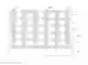
FIG. 1 is the cross sectional view of an inductive element formed by interconnecting the through silicon vias by means of through silicon via technology of the present invention.
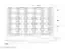
FIG. 2 is the top view of an embodiment integrating an inductive element with a analog or logic circuit of the present invention.
FIG. 3 is the schematic view when an inductive element works according to the present invention.
DETAILED DESCRIPTION OF THE INVENTION
An exemplary embodiment of the present invention is further detailed herein by referring to the drawings. The reference drawings are the schematic diagrams of the ideal embodiments of the present invention. The embodiments below are for description only rather than restricting the present invention.
Provide a semiconductor and several silicon wafers with through silicon vias and finished interconnection joints. In the embodiment, five silicon wafers with through silicon vias structure and finished interconnection joints are provided.
Next, stack and interconnect the five silicon wafers alternatively on the semiconductor substrate, as shown in FIG. 1, the semiconductor substrate 100 can be monocrystalline or polycrystalline silicon or silicon on insulators (SOI). 101, 102, 103, 104 and 105 are the five silicon wafers with through silicon vias and interconnection joints finished in the embodiment. 106 is the metal conductor after the through silicon via interconnection, wherein the metal conductor 106 comprises a conductive layer and an insulation layer isolating the conductive layer from the through silicon via surface. a and b are two measurement nodes introduced in the embodiment.
The inductive element provided by the present invention, which is used to form through silicon via interconnections, is compatible with simulation or logic circuits. FIG. 2 is the top view when integrating the inductive element provided by the embodiment of the present invention with a simulation or logic circuit. As shown in FIG. 2, 200 is a semiconductor substrate made of monocrystalline or polycrystalline silicon, wherein 201 is logic or simulation circuit, 203 is the interconnection metal conductor between measurement nodes a and b, which can be made of aluminium or copper, and 204 is the interconnection metal conductor between measurements c and d, which can be made of aluminium or copper.
FIG. 3 is the schematic diagram when the inductive element provided by the embodiment of the present invention, wherein 301 and 302 are the interconnection metal conductors between measurement nodes a, b and c, d respectively. Connecting the measurement nodes a, b, c and d in different schemes, inductive elements with different inductances can be made. Two connection schemes are provided in the embodiment.
Scheme 1: applying a specific current between measurement nodes c and d, the current flows through the metal conductor 302 and forms an electromagnetic field around the metal conductor 302, thus the metal conductor 301 between measurement nodes a and b is an inductive element.
Scheme 2: connect measurement nodes c and d in a short circuit method, and then the metal conductor 302 can form a closed loop to be an inductive element capable of forming mutual inductance with the inductive element formed by the metal conductor 301.
As described above, there are many significantly different embodiments without deviating from the spirit and scope of the present invention. It shall be understood that the present invention are not limited to the specific embodiments described in the Specification except those limited by the Claims herein.
Industrial Applicability
The inductive element formed by means of the special through silicon via interconnection by using through silicon via technology features advantages such as high inductance and density. Moreover, the through silicon via interconnection integrated process forming the inductive element is compatible with ordinary through silicon interconnection integrated process without any other steps, thus making the process simple and steady. The inductive element of the present invention is applicable to the through silicon via interconnection package manufacturing of various chips, especially the package manufacturing of power control chip and radio-frequency chip.
Claims
1. A process for creating an inductive element comprising:
a) applying a specific current between a first set of measurement nodes;
b) forming an electromagnetic field around a metal conductor; and
c) creating an inductive element between a second set of measurement nodes.
2. The process as in claim 1, wherein said step of creating an inductive element comprises providing at least one semiconductor.
3. The process as in claim 1, wherein said step of providing at least one semiconductor comprises:
stacking and interconnecting a plurality of silicon wafers alternatively on a semiconductor substrate.
4. The process as in claim 3, wherein said step of providing at least one semiconductor comprises providing at least one monocrystalline silicon or monocrystalline silicon on an insulator.
5. The process as in claim 3, wherein said step of providing at least one semiconductor comprises providing at least one polycrystalline silicon or polycrystalline silicon on an insulator.
6. A process for creating an inductive loop comprising:
a) connecting a first set of measurement nodes in a short circuit method;
b) forming a closed loop around a metal conductor to form an inductive element;
c) forming mutual inductance with said inductive element being formed by said metal conductor.
7. The process as in claim 6, wherein said step of forming an inductive element comprises providing at least one semiconductor.
8. The process as in claim 6, wherein said step of providing at least one semiconductor comprises:
stacking and interconnecting a plurality of silicon wafers alternatively on a semiconductor substrate.
9. The process as in claim 8, wherein said step of providing at least one semiconductor comprises providing at least one monocrystalline silicon or monocrystalline silicon on an insulator.
10. The process as in claim 6, wherein said step of providing at least one semiconductor comprises providing at least one polycrystalline silicon or polycrystalline silicon on an insulator.
Images & Drawings included:

Sources:
- United States Patent and Trademark Office - verify current appl. status at the USPTO↗
Recent applications in this class:
- » 20250266301 2025-08-21
SEMICONDUCTOR MANUFACTURING DEVICE AND METHOD OF MANUFACTURING SEMICONDUCTOR DEVICE - » 20250253193 2025-08-07
SEMICONDUCTOR DEVICE AND FABRICATION METHOD THEREOF - » 20250233027 2025-07-17
METHOD AND APPARATUS FOR EVALUATING INFLUENCE OF PROCESS ON SEMICONDUCTOR DEVICE PERFORMANCE AND APPLICATION THEREOF - » 20250233026 2025-07-17
SEMICONDUCTOR DEVICE AND METHOD FOR FABRICATING THE SAME - » 20250218874 2025-07-03
ANALYSIS METHOD FOR SEMICONDUCTOR DEVICE, AND ANALYSIS DEVICE THEREFOR - » 20250201637 2025-06-19
DEVICES AND METHODS FOR TESTING DIES WITH OFF-DIE CLOCKS - » 20250174498 2025-05-29
Die-Level Parametric Prediction Boosting Method and Die-Level Parametric Prediction Boosting System for Improving Prediction Accuracy by Incorporating a Wafer Map Distribution - » 20250174497 2025-05-29
Die-Level Parametric Prediction Boosting Method and System for Improving Prediction Accuracy by Incorporating Physical Location Parametric Data - » 20250157860 2025-05-15
INTEGRATED CIRCUIT PAD WITH MULTIPLE PROBING AREAS AND METHOD OF PROBING AN INTEGRATED CIRCUIT - » 20250140618 2025-05-01
PIXEL ARRAY SUBSTRATE AND FABRICATION METHOD OF DISPLAY DEVICE
Recent applications for this Assignee:
- » 20250236538 2025-07-24
Ammonia-driven hydrogel dehydration-desalination method - » 20250215598 2025-07-03
LEVELING AGENT, COMPOSITION, AND APPLICATION THEREOF - » 20250205304 2025-06-26
CD300LD INHIBITOR AND USE THEREOF IN THE PREPARATION OF TUMOR IMMUNOTHERAPY PRODUCTS - » 20250163107 2025-05-22
FUSION PROTEIN AND USE THEREOF - » 20250154146 2025-05-15
PROTEIN DEGRADERS DEVELOPED ON BASIS OF BCL-2 FAMILY PROTEIN LIGAND COMPOUNDS AND USE THEREOF - » 20250115941 2025-04-10
Exposure device for exposing microorganisms to gaseous pollutants and detection system thereof - » 20250115894 2025-04-10
Three-dimensional model of exposed microbial membranes at gas-liquid interface and preparation method thereof - » 20250060344 2025-02-20
Semi-online analytical apparatus for measuring atmospheric trace nitrogen-containing organic components - » 20250059120 2025-02-20
VISIBLE-LIGHT-MEDIATED ONE-STEP METHOD FOR PREPARING PHENOL AND CYCLOHEXANONE FROM CYCLOHEXYLBENZENE - » 20250040196 2025-01-30
FIN FIELD-EFFECT TRANSISTOR DEVICE WITH HYBRID CONDUCTION MECHANISM