Semiconductor device with encapsulated lead frame contact area and related methods
US20150348879A1
2015-12-03
14/293,364
2014-06-02
✅ Patent granted
US 9,490,146 B2
2016-11-08
-
-
Mark Tornow | Abbigale Boyle
Allen, Dyer, Doppelt, Milbrath & Gilchrist, P.A.
2034-06-06
Abstract:
A semiconductor device may include an IC, and lead frame contact areas adjacent the IC. Each lead frame contact area may have a lead opening. The semiconductor device may include bond wires, each bond wire coupling a respective lead frame contact area with the IC. The semiconductor device may include encapsulation material surrounding the IC, the lead frame contact areas, and the bond wires, and leads. Each lead may extend through a respective lead opening and outwardly from the encapsulation material.
Assignee:
- STMicroelectronics, Inc. 33 🇵🇭 Calamba City, Philippines
- STMicroelectronics, Inc. 10 🇵🇭 Calamba, Laguna, Philippines
Applicant:
Interested in similar patents?
Get notified when new applications in this technology area are published.
Classification:
H01L23/49513 » CPC main
Details of semiconductor or other solid state devices; Arrangements for conducting electric current to or from the solid state body in operation, e.g. leads, terminal arrangements ; Selection of materials therefor consisting of soldered constructions; Lead-frames or other flat leads characterised by the die pad having bonding material between chip and die pad
H01L24/49 » CPC further
Arrangements for connecting or disconnecting semiconductor or solid-state bodies; Methods or apparatus related thereto; Means for bonding being attached to, or being formed on, the surface to be connected, e.g. chip-to-package, die-attach, "first-level" interconnects; Manufacturing methods related thereto; Wire connectors; Manufacturing methods related thereto; Structure, shape, material or disposition of the wire connectors after the connecting process of a plurality of wire connectors
H01L23/49582 » CPC further
Details of semiconductor or other solid state devices; Arrangements for conducting electric current to or from the solid state body in operation, e.g. leads, terminal arrangements ; Selection of materials therefor consisting of soldered constructions; Lead-frames or other flat leads characterised by the materials of the lead frames or layers thereon Metallic layers on lead frames
H01L2224/85801 » CPC further
Indexing scheme for arrangements for connecting or disconnecting semiconductor or solid-state bodies and methods related thereto as covered by; Methods for connecting semiconductor or other solid state bodies using means for bonding being attached to, or being formed on, the surface to be connected using a wire connector; Bonding techniques Soldering or alloying
H01L21/4825 » CPC main
Processes or apparatus adapted for the manufacture or treatment of semiconductor or solid state devices or of parts thereof; Manufacture or treatment of semiconductor devices or of parts thereof the devices having at least one potential-jump barrier or surface barrier, e.g. PN junction, depletion layer or carrier concentration layer; Manufacture or treatment of parts, e.g. containers, prior to assembly of the devices, using processes not provided for in a single one of the subgroups -; Conductive parts; Flat leads, e.g. lead frames with or without insulating supports Connection or disconnection of other leads to or from flat leads, e.g. wires, bumps, other flat leads
H01L23/4952 » CPC further
Details of semiconductor or other solid state devices; Arrangements for conducting electric current to or from the solid state body in operation, e.g. leads, terminal arrangements ; Selection of materials therefor consisting of soldered constructions; Lead-frames or other flat leads; Additional leads the additional leads being a bump or a wire
H01L23/3107 » CPC further
Details of semiconductor or other solid state devices; Encapsulations, e.g. encapsulating layers, coatings, e.g. for protection characterised by the arrangement or shape the device being completely enclosed
H01L24/85 » CPC further
Arrangements for connecting or disconnecting semiconductor or solid-state bodies; Methods or apparatus related thereto; Methods for connecting semiconductor or other solid state bodies using means for bonding being attached to, or being formed on, the surface to be connected using a wire connector
H01L2924/14 » CPC further
Indexing scheme for arrangements or methods for connecting or disconnecting semiconductor or solid-state bodies as covered by; Details of semiconductor or other solid state devices to be connected; Device type Integrated circuits
H01L23/495 IPC
Details of semiconductor or other solid state devices; Arrangements for conducting electric current to or from the solid state body in operation, e.g. leads, terminal arrangements ; Selection of materials therefor consisting of soldered constructions Lead-frames or other flat leads
H01L21/48 IPC
Processes or apparatus adapted for the manufacture or treatment of semiconductor or solid state devices or of parts thereof; Manufacture or treatment of semiconductor devices or of parts thereof the devices having at least one potential-jump barrier or surface barrier, e.g. PN junction, depletion layer or carrier concentration layer Manufacture or treatment of parts, e.g. containers, prior to assembly of the devices, using processes not provided for in a single one of the subgroups -
H01L21/56 » CPC further
Processes or apparatus adapted for the manufacture or treatment of semiconductor or solid state devices or of parts thereof; Manufacture or treatment of semiconductor devices or of parts thereof the devices having at least one potential-jump barrier or surface barrier, e.g. PN junction, depletion layer or carrier concentration layer; Assembly of semiconductor devices using processes or apparatus not provided for in a single one of the subgroups - , e.g. sealing of a cap to a base of a container Encapsulations, e.g. encapsulation layers, coatings
H01L23/31 IPC
Details of semiconductor or other solid state devices; Encapsulations, e.g. encapsulating layers, coatings, e.g. for protection characterised by the arrangement or shape
H01L23/00 IPC
Details of semiconductor or other solid state devices
H01L23/49517 » CPC further
Details of semiconductor or other solid state devices; Arrangements for conducting electric current to or from the solid state body in operation, e.g. leads, terminal arrangements ; Selection of materials therefor consisting of soldered constructions; Lead-frames or other flat leads Additional leads
H01L23/49537 » CPC further
Details of semiconductor or other solid state devices; Arrangements for conducting electric current to or from the solid state body in operation, e.g. leads, terminal arrangements ; Selection of materials therefor consisting of soldered constructions; Lead-frames or other flat leads Plurality of lead frames mounted in one device
H01L23/49541 » CPC further
Details of semiconductor or other solid state devices; Arrangements for conducting electric current to or from the solid state body in operation, e.g. leads, terminal arrangements ; Selection of materials therefor consisting of soldered constructions; Lead-frames or other flat leads Geometry of the lead-frame
H01L24/48 » CPC further
Arrangements for connecting or disconnecting semiconductor or solid-state bodies; Methods or apparatus related thereto; Means for bonding being attached to, or being formed on, the surface to be connected, e.g. chip-to-package, die-attach, "first-level" interconnects; Manufacturing methods related thereto; Wire connectors; Manufacturing methods related thereto; Structure, shape, material or disposition of the wire connectors after the connecting process of an individual wire connector
H01L2224/73265 » CPC further
Indexing scheme for arrangements for connecting or disconnecting semiconductor or solid-state bodies and methods related thereto as covered by; Means for bonding being of different types provided for in two or more of groups; Location after the connecting process on different surfaces Layer and wire connectors
H01L2224/8385 » CPC further
Indexing scheme for arrangements for connecting or disconnecting semiconductor or solid-state bodies and methods related thereto as covered by; Methods for connecting semiconductor or other solid state bodies using means for bonding being attached to, or being formed on, the surface to be connected using a layer connector; Bonding techniques using a polymer adhesive, e.g. an adhesive based on silicone, epoxy, polyimide, polyester
H01L2224/92247 » CPC further
Indexing scheme for arrangements for connecting or disconnecting semiconductor or solid-state bodies and methods related thereto as covered by; Methods for connecting semiconductor or solid state bodies including different methods provided for in two or more of groups - ; Specific sequence of method steps; Connecting different surfaces of the semiconductor or solid-state body with connectors of different types; Sequential connecting processes the first connecting process involving a layer connector the second connecting process involving a wire connector
H01L2924/00014 » CPC further
Indexing scheme for arrangements or methods for connecting or disconnecting semiconductor or solid-state bodies as covered by; Technical content checked by a classifier the subject-matter covered by the group, the symbol of which is combined with the symbol of this group, being disclosed without further technical details
H01L2924/181 » CPC further
Indexing scheme for arrangements or methods for connecting or disconnecting semiconductor or solid-state bodies as covered by; Details of package parts other than the semiconductor or other solid state devices to be connected Encapsulation
H01L24/83 » CPC further
Arrangements for connecting or disconnecting semiconductor or solid-state bodies; Methods or apparatus related thereto; Methods for connecting semiconductor or other solid state bodies using means for bonding being attached to, or being formed on, the surface to be connected using a layer connector
H01L24/32 » CPC further
Arrangements for connecting or disconnecting semiconductor or solid-state bodies; Methods or apparatus related thereto; Means for bonding being attached to, or being formed on, the surface to be connected, e.g. chip-to-package, die-attach, "first-level" interconnects; Manufacturing methods related thereto; Layer connectors, e.g. plate connectors, solder or adhesive layers; Manufacturing methods related thereto; Structure, shape, material or disposition of the layer connectors after the connecting process of an individual layer connector
H01L2924/01013 » CPC further
Indexing scheme for arrangements or methods for connecting or disconnecting semiconductor or solid-state bodies as covered by; Chemical elements Aluminum [Al]
H01L2924/01029 » CPC further
Indexing scheme for arrangements or methods for connecting or disconnecting semiconductor or solid-state bodies as covered by; Chemical elements Copper [Cu]
Description
TECHNICAL FIELD
The present disclosure relates to the field of electronic devices, and, more particularly, to semiconductor devices and related methods.
BACKGROUND
In electronic devices with integrated circuits (ICs), the ICs are typically mounted onto circuit boards. In order to electrically couple connections between the circuit board and the IC, the IC is typically “packaged.” The IC packaging usually provides a small encasement for physically protecting the IC and provides contact pads for coupling to the circuit board. In some applications, the packaged IC may be coupled to the circuit board via wire bonds or solder bumps.
One approach to IC packaging comprises a quad-flat no-leads (QFN) package. The QFN package may provide some advantages, such as reduced lead inductance, a near chip scale footprint, thin profile, and low weight. Also, the QFN package typically includes perimeter I/O pads to ease circuit board trace routing, and the exposed copper die-pad technology offers enhanced thermal and electrical performance. QFN packaging may be well suited for applications where size, weight, and thermal and electrical performance are important.
Some IC packages may provide less than desirable reliability when subjected to high stress environments. For example, the IC package mounted onto a PCB may be subjected to vibrations, shocks and PCB bending that would result in the breaking of solder joint connection between the IC package and the PCB. Some approaches to IC packages, such as QFN, may not be functional after being subjected to continuous vibration and/or shock.
SUMMARY
Generally speaking, a semiconductor device may include at least one IC, and a plurality of lead frame contact areas adjacent the at least one IC. Each lead frame contact area may have a lead opening therein. The semiconductor device may include a plurality of bond wires. Each bond wire may couple a respective lead frame contact area with the at least one IC. The semiconductor device may include encapsulation material surrounding the at least one IC, the plurality of lead frame contact areas, and the plurality of bond wires, and a plurality of leads. Each lead may extend through a respective lead opening and outwardly from the encapsulation material.
In particular, semiconductor device may further include a plurality of solder joints, each solder joint attaching a respective lead within a corresponding lead opening. Each of the lead openings may comprise a lead through-opening extending through a corresponding lead frame contact area, and each of the solder joints may fill a corresponding lead through-opening. Each of the solder joints may be laterally spaced outwardly from a respective bond wire. Each of the solder joints may be a ball shape, for example.
In some embodiments, the semiconductor device may further comprise at least one IC die pad below the at least one IC. The semiconductor device may also comprise an adhesive layer between the at least one IC and the at least one IC die pad. For example, each lead frame contact area may have a rectangular shape. The plurality of lead frame contact areas and the plurality of leads may comprise copper.
Another aspect is directed to an electronic device. The electronic device may include a semiconductor device, and a printed circuit board (PCB) carrying the semiconductor device. The semiconductor device may include at least one IC, and a plurality of lead frame contact areas adjacent the at least one IC. Each lead frame contact area may have a lead opening therein. The semiconductor device may include a plurality of bond wires, each bond wire coupling a respective lead frame contact area with the at least one IC, and encapsulation material surrounding the at least one IC, the plurality of lead frame contact areas, and the plurality of bond wires. The semiconductor device may include a plurality of leads, each lead extending through a respective lead opening and outwardly from the encapsulation material.
Another aspect is directed to a method for making a semiconductor device. The method may include forming a plurality of lead frame contact areas adjacent at least one IC, each lead frame contact area having a lead opening therein, and coupling a respective bond wire between each lead frame contact area and the at least one IC. The method may include surrounding the at least one IC, the plurality of lead frame contact areas, and the plurality of bond wires with an encapsulation material, and coupling each of a plurality of leads to extend through a respective lead opening and outwardly from the encapsulation material.
BRIEF DESCRIPTION OF THE DRAWINGS
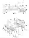
FIG. 1 is a schematic diagram of a cross-sectional view of an electronic device, according to the present disclosure.
FIG. 2 is a schematic diagram of a perspective view of the semiconductor device of FIG. 1, without the bond wires, the IC, and the adhesive layer, according to the present disclosure.
FIG. 3 is a schematic diagram of another perspective view of the semiconductor device of FIG. 1, without the leads, according to the present disclosure.
FIG. 4 is a schematic diagram of yet another perspective view of the semiconductor device of FIG. 1, before lead cutting/trimming, without the bond wires, the IC, and the adhesive layer, according to the present disclosure.
FIG. 5 is a schematic diagram of a perspective view of a step for making a semiconductor device, according to the present disclosure.
FIG. 6 is a schematic diagram of a perspective view of a step for making a semiconductor device, without the bond wires, the IC, and the adhesive layer, according to the present disclosure.
FIG. 7 is a schematic diagram of a side view of a step for making a semiconductor device, without the bond wires, the IC, and the adhesive layer, according to the present disclosure.
FIG. 8 is a schematic diagram of a side view of a step for making a semiconductor device, without the bond wires, the IC, and the adhesive layer, according to the present disclosure.
DETAILED DESCRIPTION
The present disclosure will now be described more fully hereinafter with reference to the accompanying drawings, in which several embodiments of the present disclosure are shown. This present disclosure may, however, be embodied in many different forms and should not be construed as limited to the embodiments set forth herein. Rather, these embodiments are provided so that this disclosure will be thorough and complete, and will fully convey the scope of the present disclosure to those skilled in the art. Like numbers refer to like elements throughout.
Referring initially to FIGS. 1-3, an electronic device 30 according to the present disclosure is now described. The electronic device 30 illustratively includes a semiconductor device 10, and a PCB 31 carrying the semiconductor device. The semiconductor device 10 includes an IC 11, and a plurality of lead frame contact areas 18a-18h adjacent the IC. Each lead frame contact area 18a-18h may have a lead opening therein. The semiconductor device 10 illustratively includes a plurality of bond wires 14a-14b, each bond wire coupling a respective lead frame contact area 18a-18h with the IC 11.
The semiconductor device 10 also illustratively includes encapsulation material 17 surrounding the IC 11, the plurality of lead frame contact areas 18a-18h, and the plurality of bond wires 14a-14b. For example, the encapsulation material 17 may comprise an electrically insulating resin (i.e. dielectric material). The semiconductor device 10 also illustratively includes a plurality of leads 16a-16h, each lead extending through a respective lead opening and outwardly from the encapsulation material 17. The plurality of lead frame contact areas 18a-18h and the plurality of leads 16a-16h may comprise copper, aluminum, for example.
The leads 16a-16h are coupled (e.g. soldered) to the PCB 31 via contact pads 32. Advantageously, the leads 16a-16h are flexible and mechanically robust. Accordingly, when the PCB 31 is subjected to vibration, shock, and bending, there is a reduced risk of any break or crack occurring in the outside solder joint connection between the leads 16a-16h and the PCB 31.
In particular, the semiconductor device 10 illustratively includes a plurality of solder joints 15a-15h, each solder joint attaching a respective lead 16a-16h within a corresponding lead opening. Each of the lead openings may comprise a lead through-opening extending through a corresponding lead frame contact area 18a-18h. In other words, the lead openings may completely extend through the lead frame contact areas 18a-18h, thereby defining a passageway therethrough.
Each of the solder joints 15a-15h may fill a corresponding lead through-opening. Also, as in the illustrated embodiments, each of the solder joints 15a-15h may be laterally spaced outwardly from a respective bond wire 14a-14b. Each of the solder joints 15a-15h may be a ball shape, for example. Of course, in other embodiments, the solder joints 15a-15h may have other shapes and forms.
In the illustrated embodiment, the semiconductor device 10 includes an IC die pad 13 below the IC 11, and an adhesive layer 12 between the IC and the IC die pad. The IC die pad 13 may comprise copper or aluminum. For example, in the illustrated embodiment, each lead frame contact area 18a-18h has a rectangular shape.
Another aspect is directed to a semiconductor device 10. The semiconductor device 10 may include at least one IC 11, and a plurality of lead frame contact areas 18a-18h adjacent the at least one IC. Each lead frame contact area 18a-18h may have a lead opening therein. The semiconductor device 10 may include a plurality of bond wires 14a-14b, each bond wire coupling a respective lead frame contact area 18a-18h with the at least one IC 11, and encapsulation material 17 surrounding the at least one IC, the plurality of lead frame contact areas, and the plurality of bond wires, and a plurality of leads 16a-16h, each lead extending through a respective lead opening and outwardly from the encapsulation material.
Another aspect is directed to a method for making a semiconductor device 10. The method may include forming a plurality of lead frame contact areas 18a-18h adjacent at least one IC 11, each lead frame contact area having a lead opening therein, coupling a respective bond wire 14a-14b between each lead frame contact area and the at least one IC, surrounding the at least one IC, the plurality of lead frame contact areas, and the plurality of bond wires with an encapsulation material 17, and coupling each of a plurality of leads 16a-16h to extend through a respective lead opening and outwardly from the encapsulation material.
Referring now additionally to FIGS. 4-8, a method for making the semiconductor device 10 is now described. In FIG. 5, a lead frame 22 is formed, the lead frame comprising a top lead frame component defining a plurality of recesses 24a-24h and a bottom lead frame component. The plurality of recesses 24a-24h may each have a hemisphere shape. In other embodiments, the plurality of recesses 24a-24h may each have a rectangular box shape. The top lead frame component of the lead frame 22 illustratively includes the IC die pad 13, and the plurality of lead frame contact areas 18a-18h. Each of the lead frame contact areas 18a-18h defines the recess 24a-24h. The recesses 24a-24h may be formed via a half etch isotropic process. In FIG. 6, the solder joints 15a-15h are formed respectively in the recesses 24a-24h.
The method includes positioning the IC 11 on the top lead frame component, and forming a plurality of wire bonds 14a-14b between the IC and the solder joints 15a-15h. In FIGS. 6-7, the encapsulation material 17 is formed on the lead frame 22. In FIG. 8, the lead frame 22 is etched to remove a bottom portion thereof.
As perhaps best seen in FIG. 4, once the solder joints 15a-15h are formed, the flexible lead frame 21 is positioned so that each lead 16a-16h is aligned with the respective solder joint. The method then includes a solder reflow process to couple the flexible lead frame 21 and leads 16a-16h and the solder joints 15a-15h. The flexible lead frame 21 is cut to remove the bottom portion, and the package may be singulated.
Advantageously, the semiconductor device 10 provides a tapeless lead frame IC package having bottom compliant leads to absorb shock, vibration, and PCB bending, and provide improved board level reliability (BLR). In comparison to typical small outline packaged (SOP) devices, the semiconductor device 10 can have internal rows of compliant leads (applied to QFN multi-row), unlike SOP, which only has side leads. Moreover, with the disclosed process for making the semiconductor device 10, the molding process for tapeless QFN can be used. In comparison to typical tapeless QFN devices, the semiconductor device 10 can provide leads that are compliant and expected to perform better than tapeless QFN and even tape QFN in terms of BLR and lead robustness under shock, vibration and PCB/board bending.
More generally, the semiconductor device 10 provides an approach to several problems affecting the prior art devices. Prior art devices may be subject to lead/solder joint failure when subjected to shock, vibration and PCB bending. Moreover, the semiconductor device 10 may provide an approach to improving Board Level Reliability (BLR) for typical approaches that include a package soldered on PCB and subjected to bending or thermal cycling, the non-compliant leads having lower BLR performance.
Many modifications and other embodiments of the present disclosure will come to the mind of one skilled in the art having the benefit of the teachings presented in the foregoing descriptions and the associated drawings. Therefore, it is understood that the present disclosure is not to be limited to the specific embodiments disclosed, and that modifications and embodiments are intended to be included within the scope of the appended claims.
Claims
1. A semiconductor device comprising:
at least one integrated circuit (IC);
a plurality of lead frame contact areas adjacent said at least one IC, each lead frame contact area having a lead opening therein;
a plurality of bond wires, each bond wire coupling a respective lead frame contact area with said at least one IC;
encapsulation material surrounding said at least one IC, said plurality of lead frame contact areas, and said plurality of bond wires; and
a plurality of leads, each lead extending through a respective lead opening and outwardly from said encapsulation material.
2. The semiconductor device of claim 1 further comprising a plurality of solder joints, each solder joint attaching a respective lead within a corresponding lead opening.
3. The semiconductor device of claim 2 wherein each of said lead openings comprises a lead through-opening extending through a corresponding lead frame contact area; and wherein each of said solder joints fills a corresponding lead through-opening.
4. The semiconductor device of claim 2 wherein each of said solder joints is laterally spaced outwardly from a respective bond wire.
5. The semiconductor device of claim 2 wherein each of said solder joints has a ball shape.
6. The semiconductor device of claim 1 further comprising at least one IC die pad below said at least one IC.
7. The semiconductor device of claim 6 further comprising an adhesive layer between said at least one IC and said at least one IC die pad.
8. The semiconductor device of claim 1 wherein each lead frame contact area has a rectangular shape.
9. The semiconductor device of claim 1 wherein said plurality of lead frame contact areas and said plurality of leads comprise copper.
10. An electronic device comprising:
a semiconductor device comprising
at least one integrated circuit (IC),
a plurality of lead frame contact areas adjacent said at least one IC, each lead frame contact area having a lead opening therein,
a plurality of bond wires, each bond wire coupling a respective lead frame contact area with said at least one IC,
encapsulation material surrounding said at least one IC, said plurality of lead frame contact areas, and said plurality of bond wires, and
a plurality of leads, each lead extending through a respective lead opening and outwardly from said encapsulation material; and
a printed circuit board carrying said semiconductor device.
11. The electronic device of claim 10 wherein said semiconductor device comprises a plurality of solder joints, each solder joint attaching a respective lead within a corresponding lead opening.
12. The electronic device of claim 11 wherein each of said lead openings comprises a lead through-opening extending through a corresponding lead frame contact area; and wherein each of said solder joints fills a corresponding lead through-opening.
13. The electronic device of claim 11 wherein each of said solder joints is laterally spaced outwardly from a respective bond wire.
14. The electronic device of claim 10 wherein said semiconductor device comprises at least one IC die pad below said at least one IC.
15. A method for making a semiconductor device comprising:
forming a plurality of lead frame contact areas adjacent at least one integrated circuit (IC), each lead frame contact area having a lead opening therein;
coupling a respective bond wire between each lead frame contact area and the at least one IC;
surrounding the at least one IC, the plurality of lead frame contact areas, and the plurality of bond wires with an encapsulation material; and
coupling each of a plurality of leads to extend through a respective lead opening and outwardly from the encapsulation material.
16. The method of claim 15 further comprising forming a plurality of solder joints, each solder joint attaching a respective lead within a corresponding lead opening.
17. The method of claim 16 wherein each of the lead openings comprises a lead through-opening extending through a corresponding lead frame contact area; and wherein each of the solder joints fills a corresponding lead through-opening.
18. The method of claim 16 wherein each of the solder joints is laterally spaced outwardly from a respective bond wire.
19. The method of claim 16 wherein each of the solder joints has a ball shape.
20. The method of claim 15 further comprising forming at least one IC die pad below the at least one IC.
Images & Drawings included:


Sources:
- United States Patent and Trademark Office - verify current appl. status at the USPTO↗
Recent applications in this class:
- » 20250273540 2025-08-28
METHOD OF MANUFACTURING SEMICONDUCTOR DEVICES AND CORRESPONDING SEMICONDUCTOR DEVICE - » 20250201673 2025-06-19
SEMICONDUCTOR DEVICE AND METHOD OF MANUFACTURING THE SAME - » 20250183126 2025-06-05
SEMICONDUCTOR DEVICE AND METHOD FOR MANUFACTURING THE SAME - » 20250183125 2025-06-05
ELECTRONIC DEVICE AND METHOD FOR MANUFACTURING ELECTRONIC DEVICE - » 20250157893 2025-05-15
DISCRETE SEMICONDUCTOR DEVICE PACKAGE WITH LEAD FRAME CLIP - » 20250125228 2025-04-17
METHOD OF MANUFACTURING SEMICONDUCTOR DEVICES AND CORRESPONDING SEMICONDUCTOR DEVICE - » 20250112127 2025-04-03
IC ASSEMBLIES WITH METAL PASSIVATION AT BOND INTERFACES - » 20250105103 2025-03-27
SEMICONDUCTOR PACKAGE INCLUDING ONE OR MORE SOLDER JOINTS ELECTRICALLY AND MECHANICALLY COUPLING FIRST AND SECOND POWER SEMICONDUCTOR CHIPS TO A LEADFRAME PART AND METHOD FOR FABRICATING THEA SEMICONDUCTOR PACKAGE - » 20250096078 2025-03-20
SEMICONDUCTOR DEVICE AND METHOD OF MANUFACTURING THE SAME - » 20250029901 2025-01-23
COMPACT DIRECT-BONDED METAL SUBSTRATE PACKAGE
Recent applications for this Assignee:
- » 20250183136 2025-06-05
LEAD STABILIZATION IN SEMICONDUCTOR PACKAGES - » 20250183135 2025-06-05
LEAD STABILIZATION IN SEMICONDUCTOR PACKAGES - » 20240178006 2024-05-30
Method for manufacturing leadless semiconductor package with wettable flanks - » 20240162168 2024-05-16
Semiconductor device having cavities at an interface of an encapsulant and a die pad or leads - » 20240124300 2024-04-18
CAPLESS SEMICONDUCTOR PACKAGE WITH A MICRO-ELECTROMECHANICAL SYSTEM (MEMS) - » 20240113064 2024-04-04
POWER LEADFRAME PACKAGE WITH REDUCED SOLDER VOIDS - » 20230420390 2023-12-28
LEADFRAME WITH PAD ANCHORING MEMBERS AND METHOD OF FORMING THE SAME - » 20230411251 2023-12-21
THIN SUBSTRATE PACKAGE AND LEAD FRAME - » 20230275008 2023-08-31
SEMICONDUCTOR PACKAGE WITH OVERLAPPING LEADS AND DIE PAD - » 20230253213 2023-08-10
Lead frame for improving adhesive fillets on semiconductor die corners