Vehicular panel and wiring structure for vehicle
US20170151916A1
2017-06-01
15/355,149
2016-11-18
✅ Patent granted
US 10,017,133 B2
2018-07-10
-
-
Michael F McAllister
Metrolexis Law Group, PLLC
2036-11-18
Abstract:
An instrument panel as a vehicular panel includes a panel body on a surface side of which key tops are installed, a printed wiring section arranged on the surface side of the panel body, and an insulation outer layer arranged on the surface side of the panel body so as to cover the printed wiring section.
Inventors:
- Mitsunori Tsunoda 12 🇯🇵 Shizuoka, Japan
- Gaku ITO 5 🇯🇵 Shizuoka, Japan
- Tomoaki SASAKI 2 🇯🇵 Shizuoka, Japan
- Shuji KIMURA 3 🇯🇵 Shizuoka, Japan
- Taku FURUTA 23 🇯🇵 Shizuoka, Japan
- Shoichi NOMURA 8 🇯🇵 Shizuoka, Japan
Assignee:
- Yazaki Corporation 5,523 🇯🇵 Tokyo, Japan
Applicant:
Interested in similar patents?
Get notified when new applications in this technology area are published.
Classification:
H05K2201/0338 » CPC further
Indexing scheme relating to printed circuits covered by; Conductive materials; Structure of the conductor; Layered conductors or foils Layered conductor, e.g. layered metal substrate, layered finish layer, layered thin film adhesion layer
H05K2201/0338 » CPC further
Indexing scheme relating to printed circuits covered by; Conductive materials; Structure of the conductor; Layered conductors or foils Layered conductor, e.g. layered metal substrate, layered finish layer, layered thin film adhesion layer
B60R16/02 » CPC main
Electric or fluid circuits specially adapted for vehicles and not otherwise provided for; Arrangement of elements of electric or fluid circuits specially adapted for vehicles and not otherwise provided for electric constitutive elements
B60R16/0215 » CPC further
Electric or fluid circuits specially adapted for vehicles and not otherwise provided for; Arrangement of elements of electric or fluid circuits specially adapted for vehicles and not otherwise provided for electric constitutive elements; Wire harnesses Protecting, fastening and routing means therefor
H05K1/0265 » CPC further
Printed circuits; Details; Electrical arrangements not otherwise provided for; High current adaptations, e.g. printed high current conductors or using auxiliary non-printed means; Fine and coarse circuit patterns on one circuit board characterized by the lay-out of or details of the printed conductors, e.g. reinforced conductors, redundant conductors, conductors having different cross-sections
H05K1/0284 » CPC further
Printed circuits; Details Details of three-dimensional rigid printed circuit boards
H05K1/0284 » CPC further
Printed circuits; Details Details of three-dimensional rigid printed circuit boards
H05K1/181 » CPC further
Printed circuits; Printed circuits structurally associated with non-printed electric components associated with surface mounted components
H05K1/181 » CPC further
Printed circuits; Printed circuits structurally associated with non-printed electric components associated with surface mounted components
H05K3/26 » CPC further
Apparatus or processes for manufacturing printed circuits; Secondary treatment of printed circuits Cleaning or polishing of the conductive pattern
H05K3/26 » CPC further
Apparatus or processes for manufacturing printed circuits; Secondary treatment of printed circuits Cleaning or polishing of the conductive pattern
H05K3/043 » CPC further
Apparatus or processes for manufacturing printed circuits in which the conductive material is applied to the surface of the insulating support and is thereafter removed from such areas of the surface which are not intended for current conducting or shielding the conductive material being removed mechanically, e.g. by punching by using a moving tool for milling or cutting the conductive material
H05K3/045 » CPC further
Apparatus or processes for manufacturing printed circuits in which the conductive material is applied to the surface of the insulating support and is thereafter removed from such areas of the surface which are not intended for current conducting or shielding the conductive material being removed mechanically, e.g. by punching by making a conductive layer having a relief pattern, followed by abrading of the raised portions
H05K3/125 » CPC further
Apparatus or processes for manufacturing printed circuits in which conductive material is applied to the insulating support in such a manner as to form the desired conductive pattern using printing techniques to apply the conductive material by ink-jet printing or drawing by dispensing by ink-jet printing
H05K3/247 » CPC further
Apparatus or processes for manufacturing printed circuits; Secondary treatment of printed circuits; Reinforcing the conductive pattern; Reinforcing conductive patterns made by printing techniques or by other techniques for applying conductive pastes, inks or powders; Reinforcing other conductive patterns by such techniques Finish coating of conductors by using conductive pastes, inks or powders
H05K2201/0352 » CPC further
Indexing scheme relating to printed circuits covered by; Conductive materials; Structure of the conductor; Layered conductors or foils Differences between the conductors of different layers of a multilayer
H05K2201/0352 » CPC further
Indexing scheme relating to printed circuits covered by; Conductive materials; Structure of the conductor; Layered conductors or foils Differences between the conductors of different layers of a multilayer
H05K2201/0391 » CPC further
Indexing scheme relating to printed circuits covered by; Conductive materials; Structure of the conductor; Other aspects of conductors Using different types of conductors
H05K2201/0391 » CPC further
Indexing scheme relating to printed circuits covered by; Conductive materials; Structure of the conductor; Other aspects of conductors Using different types of conductors
H05K2201/09036 » CPC further
Indexing scheme relating to printed circuits covered by; Shape and layout; Substrate related Recesses or grooves in insulating substrate
H05K2201/09036 » CPC further
Indexing scheme relating to printed circuits covered by; Shape and layout; Substrate related Recesses or grooves in insulating substrate
H05K2201/09727 » CPC further
Indexing scheme relating to printed circuits covered by; Shape and layout; Shape and layout details of conductors covering at least two types of conductors provided for in - Varying width along a single conductor; Conductors or pads having different widths
H05K2201/09727 » CPC further
Indexing scheme relating to printed circuits covered by; Shape and layout; Shape and layout details of conductors covering at least two types of conductors provided for in - Varying width along a single conductor; Conductors or pads having different widths
H05K2201/09736 » CPC further
Indexing scheme relating to printed circuits covered by; Shape and layout; Shape and layout details of conductors covering at least two types of conductors provided for in - Varying thickness of a single conductor; Conductors in the same plane having different thicknesses
H05K2201/10053 » CPC further
Indexing scheme relating to printed circuits covered by; Details of components or other objects attached to or integrated in a printed circuit board; Types of components Switch
H05K2201/10053 » CPC further
Indexing scheme relating to printed circuits covered by; Details of components or other objects attached to or integrated in a printed circuit board; Types of components Switch
H05K2201/10272 » CPC further
Indexing scheme relating to printed circuits covered by; Details of components or other objects attached to or integrated in a printed circuit board; Other objects, e.g. metallic pieces Busbars, i.e. thick metal bars mounted on the PCB as high-current conductors
H05K2201/10272 » CPC further
Indexing scheme relating to printed circuits covered by; Details of components or other objects attached to or integrated in a printed circuit board; Other objects, e.g. metallic pieces Busbars, i.e. thick metal bars mounted on the PCB as high-current conductors
H05K2203/025 » CPC further
Indexing scheme relating to apparatus or processes for manufacturing printed circuits covered by; Details related to mechanical or acoustic processing, e.g. drilling, punching, cutting, using ultrasound Abrading, e.g. grinding or sand blasting
H05K2203/025 » CPC further
Indexing scheme relating to apparatus or processes for manufacturing printed circuits covered by; Details related to mechanical or acoustic processing, e.g. drilling, punching, cutting, using ultrasound Abrading, e.g. grinding or sand blasting
H05K2203/0353 » CPC further
Indexing scheme relating to apparatus or processes for manufacturing printed circuits covered by; Metal processing Making conductive layer thin, e.g. by etching
H05K2203/0353 » CPC further
Indexing scheme relating to apparatus or processes for manufacturing printed circuits covered by; Metal processing Making conductive layer thin, e.g. by etching
H05K2203/0545 » CPC further
Indexing scheme relating to apparatus or processes for manufacturing printed circuits covered by; Patterning and lithography; Masks; Details of resist; Patterning and lithography Pattern for applying drops or paste; Applying a pattern made of drops or paste
H05K2203/0545 » CPC further
Indexing scheme relating to apparatus or processes for manufacturing printed circuits covered by; Patterning and lithography; Masks; Details of resist; Patterning and lithography Pattern for applying drops or paste; Applying a pattern made of drops or paste
H05K1/02 IPC
Printed circuits Details
H05K1/02 IPC
Printed circuits Details
H05K1/18 IPC
Printed circuits Printed circuits structurally associated with non-printed electric components
H05K1/18 IPC
Printed circuits Printed circuits structurally associated with non-printed electric components
H05K3/12 IPC
Apparatus or processes for manufacturing printed circuits in which conductive material is applied to the insulating support in such a manner as to form the desired conductive pattern using printing techniques to apply the conductive material
H05K3/12 IPC
Apparatus or processes for manufacturing printed circuits in which conductive material is applied to the insulating support in such a manner as to form the desired conductive pattern using printing techniques to apply the conductive material
H05K3/04 IPC
Apparatus or processes for manufacturing printed circuits in which the conductive material is applied to the surface of the insulating support and is thereafter removed from such areas of the surface which are not intended for current conducting or shielding the conductive material being removed mechanically, e.g. by punching
H05K3/24 IPC
Apparatus or processes for manufacturing printed circuits; Secondary treatment of printed circuits Reinforcing the conductive pattern
H05K3/24 IPC
Apparatus or processes for manufacturing printed circuits; Secondary treatment of printed circuits Reinforcing the conductive pattern
Description
CROSS REFERENCE TO RELATED APPLICATION
The present application is based on, and claims priority from Japanese Patent Application No. 2015-231572, filed Nov. 27, 2015, the disclosure of which is hereby incorporated by reference herein in its entirety.
TECHNICAL FIELD
The present application relates to a vehicular panel and a wiring structure for a vehicle.
BACKGROUND ART
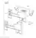
Heretofore, various proposals have been made for an electric wire arrangement of a vehicular panel that uses a wire harness (see JP H01-067809 A1. A vehicular panel having such a structure according to a conventional example is illustrated in FIG. 12. In FIG. 12, a plurality of electric components 101 are installed on the surface side of an instrument panel 100 as the vehicular panel according to the conventional example. The instrument panel 100 is composed of a panel body 100A and an outer layer 100B arranged on the surface side thereof. A wire harness WH is wired on the back side of the instrument panel 100. Electric connections between the electric components 101 are made by the wire harness WH.
SUMMARY
In the vehicular panel according to the conventional example, a wiring operation of the wire harness WH, and a connecting operation of connectors between the wire harness WH and the panel body 100A, and the like need to be performed on the back side of the panel body 100A. On the other hand, operations such as mounting of the electric components 101, and mounting of the outer layer 100B to the panel body 100A, and the like need to be performed on the surface side of the panel body 100A. Since it is necessary that operations are performed on both the surface side and the back side of the panel body 100A as such, there is a problem that workability in the manufacturing process is poor.
Accordingly, the present application was made to solve the above-described problem and it aims to provide a vehicular panel and a wiring structure for vehicle which have good workability in the manufacturing process.
A vehicular panel according to a first aspect of the present application includes a panel body on a surface side of which an electric component is installed, a printed wiring section including a conductive member arranged on the surface side of the panel body, and an insulation outer layer arranged on the surface side of the panel body so as to cover the printed wiring section.
A wiring structure for vehicle according to a second aspect of the present application includes a panel body on a surface side of which an electric component is installed, an insulation outer layer arranged on the surface side of the panel body, and a printed wiring section including a conductive member arranged between the panel body and the insulation outer layer.
With the vehicular panel according to the first aspect of the present application and the wiring structure for vehicle according to the second aspect of the present application, a mounting operation of the electric component, an arranging operation of the printed wiring section, and a mounting operation of the insulation outer layer to the panel body can be performed from the surface side of the panel body, and therefore, workability in the manufacturing process is good.
BRIEF DESCRIPTION OF DRAWINGS
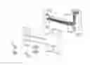
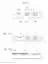
FIG. 1 is an exploded perspective view of an instrument panel according to an embodiment.
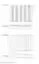
FIG. 2A is a plan view of a main part of printed wiring sections of the instrument panel according to the embodiment (in which printed wiring sections 3 are illustrated as being hatched).
FIG. 2B is a cross-sectional view of the main part of the printed wiring sections of the instrument panel according to the embodiment.
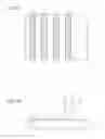
FIG. 3A is a plan view of the main part for explanation of a manufacturing process of the printed wiring sections of the instrument panel according to the embodiment.
FIG. 3B is a cross-sectional view of the main part for explanation of a manufacturing process of the printed wiring sections of the instrument panel according to the embodiment.
FIG. 4A is a plan view of the main part for explanation of a manufacturing process of the printed wiring sections of the instrument panel according to the embodiment (in Which a conductive member 30 is illustrated as being hatched).
FIG. 4B is a cross-sectional view of the main part for explanation of a manufacturing process of the printed wiring sections of the instrument panel according to the embodiment.
FIG. 5 is a cross-sectional view of the main part for explanation of a manufacturing process of the printed wiring sections of the instrument panel according to the embodiment.
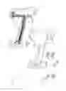
FIG. 6A is a plan view of a main part of printed wiring sections of the instrument panel according to a comparative example 1 (in which printed wiring sections 3 are illustrated as being hatched).
FIG. 6B is a cross-sectional view of the main part of the printed wiring sections of the instrument panel according to the comparative example 1.
FIG. 7A is a plan view of a main part for explanation of a manufacturing process of an electronic component mounting portion of the printed wiring sections of the instrument panel according to a first modification (in which the printed wiring sections 3 are illustrated as being hatched).
FIG. 7B is a cross-sectional view of the main part for explanation of the manufacturing process of the electronic component mounting portion of the printed wiring sections of the instrument panel according to the first modification.
FIG. 8A is a plan view of the main part for explanation of a manufacturing process of the electronic component mounting portion of the printed wiring sections of the instrument panel according to the first modification (in which the conductive members 30 are illustrated as being hatched).
FIG. 8B is a cross-sectional view of the main part for explanation of the manufacturing process of the electronic component mounting portion of the printed wiring sections of the instrument panel according to the first modification.
FIG. 9A is a plan view of the main part for explanation of a manufacturing process of the printed wiring sections of the instrument panel according to the first modification (in which printed wiring sections 3 are illustrated as being hatched).
FIG. 9B is a cross-sectional view of the main part for explanation of the manufacturing process of the printed wiring sections of the instrument panel according to the first modification.
FIG. 10 is a cross-sectional view of a main part of a portion in which a printed wiring section for a small current and a printed wiring section for a large current exist in the instrument panel according to a second modification.
FIG. 11A is a cross-sectional view of a main part of the printed wiring sections of the instrument panel according to a comparative example 2.
FIG. 11B is a cross-sectional view of a main part of the printed wiring sections of the instrument panel according to a comparative example 3.
FIG. 12 is a perspective view of an instrument panel and a wire harness according to a conventional example.
DESCRIPTION OF EMBODIMENTS
Hereinafter, a vehicular panel according to an embodiment will be explained based on the drawings.
(Overall Structure)
An instrument panel 1 as the vehicular panel according to the embodiment and a wiring structure for vehicle applied thereto will be explained.
As illustrated in FIG. 1, the instrument panel 1 as the vehicular panel according to the embodiment includes a panel body 2, a printed wiring section 3 arranged on the surface of the panel body 2, and an insulation outer layer 4 arranged on the surface side of the panel body 2 so as to cover the printed wiring section 3.
Key tops 6 of switches as a plurality of electric components are installed on the surface side of the panel body 2.
The printed wiring section 3 is arranged by directly printing a conductive member (conductive ink, conductive paste, or the like) on the surface of the panel body 2. An electronic component 7 for the switches is mounted on a terminal of the printed wiring section 3. Fabrication of the printed wiring section 3 and mounting of the electronic component 7 will be described in detail below.
The insulation outer layer 4 is formed in approximately the same shape as a surface shape of the panel body 2. The insulation outer layer 4 covers almost entirety of the panel body 2 except for the installation regions of the key tops 6.
Assembling order of the instrument panel 1 will be explained. An intended printed wiring section 3 is formed such as by spraying conductive ink with an ink jet nozzle (not illustrated) onto the surface of the panel body 2. Next, the key tops 6 of the switches are mounted on the panel body 2 from its surface side. Then, the insulation outer layer 4 is affixed to the surface side of the panel body 2. Next, bezels 8 are put on the surface side of the panel body 2 so as to cover the parting lines. With this, assembly of the instrument panel 1 is completed.
As explained above, the instrument panel 1 includes the panel body 2 on the surface side of which the key tops 6 as the electric components are installed, the printed wiring section 3 arranged on the surface of the panel body 2, and the insulation outer layer 4 arranged on the surface side of the panel body 2 so as to cover the printed wiring section 3. As the vehicular wiring structure, it has a structure such that it includes the panel body 2 on the surface side of which the key tops 6 as the electric components are installed, the insulation outer layer 4 arranged on the surface side of the panel body 2, and the printed wiring section 3 arranged between the panel body 2 and the insulation outer layer 4.
Therefore, mounting of the key tops 6 as the electric components, an arranging operation of the printed wiring section 3, and a mounting operation of the insulation outer layer 4 onto the panel body 4 can all be performed from the surface side of the panel body 2, and thus, workability in the manufacturing process is good.
Since the insulation outer layer 4 has a design function of the instrument panel 1 and at the same time performs insulation and protection of the printed wiring section 3, it is not necessary to provide an insulation protective film on the surface of the printed wiring section 3 separately.
In the embodiment, the printed wiring section 3 is arranged by directly printing the conductive member (such as conductive ink) on the surface of the panel body 2, but it can also be arranged for example by affixing a film on which a conductive member (such as conductive ink) is printed onto the surface of the panel body 2.
(Details of the Printed Wiring Section)
As illustrated in FIGS. 2A and 2B, routing grooves 10 are formed along the wiring patterns of the printed wiring sections 3 on the surface side of the panel body 2. The printed wiring sections 3 are respectively arranged on each of the routing grooves 10. Fabrication of the printed wiring sections 3 is as follows. First, as illustrated in FIGS. 3A and 3B, the routing grooves 10 are formed on the panel body 2. Next, as illustrated in FIGS. 4A and 4B, a conductive member (such as conductive ink) 30 is sprayed with an ink jet nozzle 20 over the entire region of the panel body 2. Then, as illustrated in FIG. 5, the entire surface region of the panel body 2 is wiped with e.g. sandpaper 21, thus removing the conductive member 30 on the surface of the panel body 2 (i.e., other than the conductive member within the routing grooves 10). With this, the printed wiring sections 3 as illustrated in FIGS. 2A and 2B are formed.
Moreover, in the plan views of FIGS. 2A, 4A, and 6A, the printed wiring sections 3 and the conductive member 30 are illustrated as being hatched for the sake of clarity.
According to such a structure, fabrication (processing) time for the printed wiring sections 3 can be shortened.
In a case of disposing the electronic component 7 on the way of a route of the printed wiring section 3, the routing groove 10 is not formed at that position. In other words, divided routing grooves 10 are formed. The electronic component 7 is arranged at the divided portion of the routing groove 10. Thus, the printed wiring section 3 on which the electronic component 7 is mounted is fabricated.
In other words, in a conventional example using a wire harness as the wiring member, there is usually a need to connect with the panel body side by a connector; however, in a case of the printed wiring section 3, it becomes possible to make an electronic connection without using a connector and the structure becomes simple.
COMPARATIVE EXAMPLE 1
In an instrument panel according to a comparative example 1 as illustrated in FIGS. 6A and 6B, a conductive member (such as conductive ink) is sprayed onto the panel body 2 along a wiring pattern with the ink jet nozzle 20. In other words, the printed wiring sections 3 are formed by drawing with the ink jet nozzle 20. Since it is necessary that all of the printed wiring sections 3 are drawn with the ink jet nozzle 20, there is a problem that the fabrication (processing) time to form the printed wiring sections 3 becomes long. In the present embodiment, such a problem is solved and it is possible to shorten the fabrication (processing) time to form the printed wiring sections 3.
(Details of the Electronic Component Arrangement and its Peripheral Printed Wiring Section)
FIGS. 7A to 9B illustrate a first modification of the embodiment. As illustrated in FIGS. 7A and 7B, a protrusion 11 is provided at a portion on which the electronic component 7 is arranged on the surface of the panel body 2. The printed wiring sections 3 are arranged at both sides of the protrusion 11.
The electronic component 7 is mounted on the protrusion 11. Lead portions 7a of the electronic component 7 are connected to the printed wiring sections 3 at both sides of the protrusion 11 such as by soldering.
Arrangement of the electronic component 7 and fabrication of the peripheral printed wiring sections 3 are as follows. First, the protrusion 11 is formed at a mounting position of the electronic component 7 on the surface of the panel body 2. Then, as illustrated in FIGS. 8A and 8B, the conductive member 30 (such as conductive ink) is sprayed with the ink jet nozzle 20 along a wiring pattern that includes an area on the protrusion 11. Since the protrusion 11 exists on the wiring pattern, the conductive member (such as conductive ink) 30 is disposed on the upper surface of the protrusion 11 also. Then, as illustrated in FIGS. 9A and 9B, only the conductive member 30 (such as conductive ink) on the upper surface of the protrusion 11 is wiped with e.g. sandpaper 21. Thus, the divided printed wiring sections 3 are formed at both sides of the protrusion 11. Next, as illustrated in FIGS. 7A and 7B, once the electronic component 7 is mounted on the protrusion 11 and the lead portions 7a of the electronic component 7 are connected to the printed wiring sections 3 such as by soldering, it is completed.
Moreover, in the plan views of FIGS. 7A, 8A, and 9A, the printed wiring sections 3 and the conductive member 30 are illustrated as being hatched for the sake of clarity.
Since spraying of the conductive member at the ink jet nozzle 20 can be performed without considering the mounting position of the electronic component 7, controlling of the ink jet nozzle 20 is easy.
(Printed Wiring Sections for Small Current and for Large Current)
FIG. 10 illustrates a second modification of the embodiment. As illustrated in FIG. 10, the printed wiring sections 3A, 3B includes large current wiring sections 3A for a large current and a small current wiring section 3B for a small current. Bus bars 12 are buried along large current routing grooves 10A at the bottom of the large current routing grooves 10A in which the printed large current wiring sections 3A are arranged.
Each of the large current wiring sections 3A includes the bus bar 12 and a conductive member (such as conductive ink) 3a arranged in the large current routing groove 10A. The small current wiring section 3B is composed only of a conductive member (such as conductive ink) arranged in the routing groove for a small current 10B.
With such a structure, by preparing a panel body 2 in which the bus bars 12 are buried, operations of the later printing process for the large current wiring sections 3A and for the small current wiring section 3B can be the same. In other words, the large current wiring sections 3A and the small current wiring section 3B can be worked on by an operation of the same printing process, and thus, work efficiency can be improved.
Instead of the bus bar 12, copper foil may be buried for each of the large current wiring sections 3A also.
COMPARATIVE EXAMPLES 2 AND 3
In a comparative example 2 as illustrated in FIG. 11A, in a case that large current wiring sections 3C and a small current wiring section 3D are formed as the printed wiring sections 3C, 3D, thickness of each of the large current wiring sections 3C is formed to be thicker and thickness of the small current wiring section 3C is formed to be thinner.
In a comparative example 3 as illustrated in FIG. 11B, in a case that large current wiring sections 3E and a small current wiring section 3F are formed as the printed wiring sections 3E, 3F, width of each of the large current wiring sections 3E is formed to be wider and width of the small current wiring section 3F is formed to be narrower.
In both of the comparative examples 2 and 3, operations of the printing process for the large current wiring sections 3C, 3E and for the small current wiring sections 3D, 3F need to be altered, and the operations become complex. The above-described structure solves the problems of these comparative examples 2 and 3, and makes it possible for operations of the printing process for the large current wiring sections 3A and for the small current wiring section 3B to be made the same.
Claims
What is claimed is:1. A vehicular panel, comprising:
a panel body on a surface side of which an electric component is installed;
a printed wiring section comprising a conductive member arranged on the surface side of the panel body; and
an insulation outer layer arranged on the surface side of the panel body so as to cover the printed wiring section.
2. The vehicular panel of claim 1, wherein
a routing groove is formed on the panel body, and
the printed wiring section is arranged in the routing groove.
3. The vehicular panel of claim 2, wherein:
the printed wiring section comprises a large current wiring section for a large current and a small current wiring section for a small current;
the routing groove includes a large current routing groove in which the large current wiring section is arranged, and a small current routing groove in which the small current wiring section is arranged;
a bus bar is buried at a bottom of the large current routing groove;
the large current wiring section comprises the bus bar and the conductive member arranged in the large current routing groove; and
the small current wiring section is composed of the conductive member arranged in the small current routing groove.
4. A wiring structure for vehicle, comprising:
a panel body on a surface side of which an electric component is installed;
an insulation outer layer arranged on the surface side of the panel body; and
a printed wiring section comprising a conductive member arranged between the panel body and the insulation outer layer.
Images & Drawings included:


Sources:
- United States Patent and Trademark Office - verify current appl. status at the USPTO↗
Recent applications in this class:
- » 20250206241 2025-06-26
ATTACHMENT STRUCTURE OF ELECTRICAL COMPONENT AND MANUFACTURING METHOD OF ATTACHMENT STRUCTURE - » 20250115195 2025-04-10
IN-VEHICLE CONTROL DEVICE, CONTROL METHOD, AND COMPUTER PROGRAM - » 20240300421 2024-09-12
VEHICLE TRIM PANEL ASSEMBLY - » 20240246497 2024-07-25
ELECTRICAL SYSTEM - » 20240217457 2024-07-04
INSTALLATION STRUCTURE FOR HIGH-VOLTAGE ELECTRICAL DEVICE INSTALLED ON FRONT SECTION OF VEHICLE - » 20240198931 2024-06-20
In-Vehicle Control Device and Manufacturing Method - » 20240101049 2024-03-28
VEHICLE CONTROL DEVICE, NON-TRANSITORY COMPUTER-READABLE STORAGE MEDIUM STORING VEHICLE CONTROL PROGRAM, AND VEHICLE CONTROL SYSTEM - » 20230406236 2023-12-21
VEHICLE DEVICE - » 20230406235 2023-12-21
VEHICLE REMOTE POWER SUPPLY SYSTEMS WITH INTEGRATED RETRACTABLE EXTENSION CORDS - » 20230242051 2023-08-03
Jumper cable device and jump start system
Recent applications for this Assignee:
- » 20250293495 2025-09-18
WIRE HARNESS - » 20250292932 2025-09-18
WIRE HARNESS AND EXTERIOR MEMBER - » 20250289379 2025-09-18
WIRE HARNESS WIRING STRUCTURE AND WIRE HARNESS - » 20250287515 2025-09-11
ELECTRONIC CONTROL UNIT - » 20250286357 2025-09-11
ELECTRONIC CONTROL UNIT - » 20250286356 2025-09-11
WATERPROOF STRUCTURE AND WIRE HARNESS - » 20250279617 2025-09-04
CONNECTOR - » 20250279616 2025-09-04
CONNECTOR - » 20250273916 2025-08-28
CONNECTOR - » 20250273894 2025-08-28
CONNECTOR