Integrated circuit die having a split solder pad
US20180053699A1
2018-02-22
15/678,186
2017-08-16
✅ Patent granted
US 10,192,798 B2
2019-01-29
-
-
William Harriston
Oblon, McClelland, Maier & Neustadt, L.L.P.
2037-08-16
Abstract:
The invention relates to an electronic system comprising:
-
- an integrated circuit die having:
- at least 2 bond pads
- a redistribution layer, said redistribution layer having:
- at least a solder pad comprising 2 portions arranged to enable an electrical connection between each other by a same solder ball placed on said solder pad, but electrically isolated of each other in the absence of a solder ball on the solder pad
- at least 2 redistribution wires, each one connecting one of the 2 portions to one of the 2 bond pads,
a second bond pad connected via a second redistribution wire to a second portion of the solder pad being dedicated to testing said integrated circuit die
- a grounded printed circuit board track, a solder ball being placed between the solder pad and the printed circuit board track.
- an integrated circuit die having:
Inventors:
- Yves DUPRAZ 5 🇨🇭 Valeyres-sous-Montagny, Switzerland
- Christoph KURATLI 2 🇨🇭 Guemmenen, Switzerland
Assignee:
- EM Microelectronic-Marin S.A. 226 🇨🇭 Marin, Switzerland
Applicant:
Interested in similar patents?
Get notified when new applications in this technology area are published.
Classification:
H01L22/32 » CPC main
Testing or measuring during manufacture or treatment; Reliability measurements, i.e. testing of parts without further processing to modify the parts as such; Structural arrangements therefor; Structural arrangements specially adapted for testing or measuring during manufacture or treatment, or specially adapted for reliability measurements Additional lead-in metallisation on a device or substrate, e.g. additional pads or pad portions, lines in the scribe line, sacrificed conductors
H01L24/05 » CPC further
Arrangements for connecting or disconnecting semiconductor or solid-state bodies; Methods or apparatus related thereto; Means for bonding being attached to, or being formed on, the surface to be connected, e.g. chip-to-package, die-attach, "first-level" interconnects; Manufacturing methods related thereto; Bonding areas ; Manufacturing methods related thereto; Structure, shape, material or disposition of the bonding areas prior to the connecting process of an individual bonding area
H01L2224/02375 » CPC further
Indexing scheme for arrangements for connecting or disconnecting semiconductor or solid-state bodies and methods related thereto as covered by; Means for bonding being attached to, or being formed on, the surface to be connected, e.g. chip-to-package, die-attach, "first-level" interconnects; Manufacturing methods related thereto; Bonding areas; Manufacturing methods related thereto; Redistribution layers [RDL] for bonding areas; Disposition of the redistribution layers Top view
H01L2224/0401 » CPC further
Indexing scheme for arrangements for connecting or disconnecting semiconductor or solid-state bodies and methods related thereto as covered by; Means for bonding being attached to, or being formed on, the surface to be connected, e.g. chip-to-package, die-attach, "first-level" interconnects; Manufacturing methods related thereto; Bonding areas; Manufacturing methods related thereto; Structure, shape, material or disposition of the bonding areas prior to the connecting process Bonding areas specifically adapted for bump connectors, e.g. under bump metallisation [UBM]
H01L23/00 IPC
Details of semiconductor or other solid state devices
H01L23/5286 » CPC further
Details of semiconductor or other solid state devices; Arrangements for conducting electric current within the device in operation from one component to another, i.e. interconnections, e.g. wires, lead frames including external interconnections consisting of a multilayer structure of conductive and insulating layers inseparably formed on the semiconductor body layout of the interconnection structure Arrangements of power or ground buses
H01L24/49 » CPC further
Arrangements for connecting or disconnecting semiconductor or solid-state bodies; Methods or apparatus related thereto; Means for bonding being attached to, or being formed on, the surface to be connected, e.g. chip-to-package, die-attach, "first-level" interconnects; Manufacturing methods related thereto; Wire connectors; Manufacturing methods related thereto; Structure, shape, material or disposition of the wire connectors after the connecting process of a plurality of wire connectors
G01R31/31715 » CPC further
Arrangements for testing electric properties; Arrangements for locating electric faults; Arrangements for electrical testing characterised by what is being tested not provided for elsewhere; Testing of electronic circuits, e.g. by signal tracer; Testing of digital circuits; Input or output aspects Testing of input or output circuits; test of circuitry between the I/C pins and the functional core, e.g. testing of input or output driver, receiver, buffer
G01R31/31937 » CPC further
Arrangements for testing electric properties; Arrangements for locating electric faults; Arrangements for electrical testing characterised by what is being tested not provided for elsewhere; Testing of electronic circuits, e.g. by signal tracer; Testing of digital circuits; Functional testing; Tester hardware, i.e. output processing circuits with comparison between actual response and known fault free response Timing aspects, e.g. measuring propagation delay
H01L23/3114 » CPC further
Details of semiconductor or other solid state devices; Encapsulations, e.g. encapsulating layers, coatings, e.g. for protection characterised by the arrangement or shape the device being completely enclosed the device being a chip scale package, e.g. CSP
G01R31/317 IPC
Arrangements for testing electric properties; Arrangements for locating electric faults; Arrangements for electrical testing characterised by what is being tested not provided for elsewhere; Testing of electronic circuits, e.g. by signal tracer Testing of digital circuits
H01L24/06 » CPC further
Arrangements for connecting or disconnecting semiconductor or solid-state bodies; Methods or apparatus related thereto; Means for bonding being attached to, or being formed on, the surface to be connected, e.g. chip-to-package, die-attach, "first-level" interconnects; Manufacturing methods related thereto; Bonding areas ; Manufacturing methods related thereto; Structure, shape, material or disposition of the bonding areas prior to the connecting process of a plurality of bonding areas
H01L24/09 » CPC further
Arrangements for connecting or disconnecting semiconductor or solid-state bodies; Methods or apparatus related thereto; Means for bonding being attached to, or being formed on, the surface to be connected, e.g. chip-to-package, die-attach, "first-level" interconnects; Manufacturing methods related thereto; Bonding areas ; Manufacturing methods related thereto; Structure, shape, material or disposition of the bonding areas after the connecting process of a plurality of bonding areas
H01L24/16 » CPC further
Arrangements for connecting or disconnecting semiconductor or solid-state bodies; Methods or apparatus related thereto; Means for bonding being attached to, or being formed on, the surface to be connected, e.g. chip-to-package, die-attach, "first-level" interconnects; Manufacturing methods related thereto; Bump connectors ; Manufacturing methods related thereto; Structure, shape, material or disposition of the bump connectors after the connecting process of an individual bump connector
H01L24/17 » CPC further
Arrangements for connecting or disconnecting semiconductor or solid-state bodies; Methods or apparatus related thereto; Means for bonding being attached to, or being formed on, the surface to be connected, e.g. chip-to-package, die-attach, "first-level" interconnects; Manufacturing methods related thereto; Bump connectors ; Manufacturing methods related thereto; Structure, shape, material or disposition of the bump connectors after the connecting process of a plurality of bump connectors
H01L2224/02371 » CPC further
Indexing scheme for arrangements for connecting or disconnecting semiconductor or solid-state bodies and methods related thereto as covered by; Means for bonding being attached to, or being formed on, the surface to be connected, e.g. chip-to-package, die-attach, "first-level" interconnects; Manufacturing methods related thereto; Bonding areas; Manufacturing methods related thereto; Redistribution layers [RDL] for bonding areas; Disposition of the redistribution layers connecting the bonding area on a surface of the semiconductor or solid-state body with another surface of the semiconductor or solid-state body
H01L2224/02377 » CPC further
Indexing scheme for arrangements for connecting or disconnecting semiconductor or solid-state bodies and methods related thereto as covered by; Means for bonding being attached to, or being formed on, the surface to be connected, e.g. chip-to-package, die-attach, "first-level" interconnects; Manufacturing methods related thereto; Bonding areas; Manufacturing methods related thereto; Redistribution layers [RDL] for bonding areas; Disposition of the redistribution layers Fan-in arrangement
H01L2224/04042 » CPC further
Indexing scheme for arrangements for connecting or disconnecting semiconductor or solid-state bodies and methods related thereto as covered by; Means for bonding being attached to, or being formed on, the surface to be connected, e.g. chip-to-package, die-attach, "first-level" interconnects; Manufacturing methods related thereto; Bonding areas; Manufacturing methods related thereto; Structure, shape, material or disposition of the bonding areas prior to the connecting process Bonding areas specifically adapted for wire connectors, e.g. wirebond pads
H01L2224/0603 » CPC further
Indexing scheme for arrangements for connecting or disconnecting semiconductor or solid-state bodies and methods related thereto as covered by; Means for bonding being attached to, or being formed on, the surface to be connected, e.g. chip-to-package, die-attach, "first-level" interconnects; Manufacturing methods related thereto; Bonding areas; Manufacturing methods related thereto; Structure, shape, material or disposition of the bonding areas prior to the connecting process of a plurality of bonding areas; Structure Bonding areas having different sizes, e.g. different heights or widths
H01L2224/06051 » CPC further
Indexing scheme for arrangements for connecting or disconnecting semiconductor or solid-state bodies and methods related thereto as covered by; Means for bonding being attached to, or being formed on, the surface to be connected, e.g. chip-to-package, die-attach, "first-level" interconnects; Manufacturing methods related thereto; Bonding areas; Manufacturing methods related thereto; Structure, shape, material or disposition of the bonding areas prior to the connecting process of a plurality of bonding areas; Shape Bonding areas having different shapes
H01L2224/1613 » CPC further
Indexing scheme for arrangements for connecting or disconnecting semiconductor or solid-state bodies and methods related thereto as covered by; Means for bonding being attached to, or being formed on, the surface to be connected, e.g. chip-to-package, die-attach, "first-level" interconnects; Manufacturing methods related thereto; Bump connectors; Manufacturing methods related thereto; Structure, shape, material or disposition of the bump connectors after the connecting process of an individual bump connector; Disposition the bump connector connecting within a semiconductor or solid-state body, i.e. connecting two bonding areas on the same semiconductor or solid-state body
H01L2924/00014 » CPC further
Indexing scheme for arrangements or methods for connecting or disconnecting semiconductor or solid-state bodies as covered by; Technical content checked by a classifier the subject-matter covered by the group, the symbol of which is combined with the symbol of this group, being disclosed without further technical details
H01L23/31 IPC
Details of semiconductor or other solid state devices; Encapsulations, e.g. encapsulating layers, coatings, e.g. for protection characterised by the arrangement or shape
G01R31/3193 IPC
Arrangements for testing electric properties; Arrangements for locating electric faults; Arrangements for electrical testing characterised by what is being tested not provided for elsewhere; Testing of electronic circuits, e.g. by signal tracer; Testing of digital circuits; Functional testing; Tester hardware, i.e. output processing circuits with comparison between actual response and known fault free response
H01L23/525 » CPC further
Details of semiconductor or other solid state devices; Arrangements for conducting electric current within the device in operation from one component to another, i.e. interconnections, e.g. wires, lead frames including external interconnections consisting of a multilayer structure of conductive and insulating layers inseparably formed on the semiconductor body with adaptable interconnections
H01L23/528 » CPC further
Details of semiconductor or other solid state devices; Arrangements for conducting electric current within the device in operation from one component to another, i.e. interconnections, e.g. wires, lead frames including external interconnections consisting of a multilayer structure of conductive and insulating layers inseparably formed on the semiconductor body layout of the interconnection structure
H01L24/48 » CPC further
Arrangements for connecting or disconnecting semiconductor or solid-state bodies; Methods or apparatus related thereto; Means for bonding being attached to, or being formed on, the surface to be connected, e.g. chip-to-package, die-attach, "first-level" interconnects; Manufacturing methods related thereto; Wire connectors; Manufacturing methods related thereto; Structure, shape, material or disposition of the wire connectors after the connecting process of an individual wire connector
Description
This application claims priority from European patent application No. 16184545.8 filed on Aug. 17, 2016, the entire disclosure of which is hereby incorporated herein by reference.
FIELD OF THE INVENTION
The invention relates to a pad for a solder ball, called solder pad, in a redistribution layer of an integrated circuit die.
BACKGROUND OF THE INVENTION
An integrated circuit (IC) die (also called chip) is classically put into a protective package acting as a mechanical interface between said integrated circuit die and a printed circuit board (PCB). A very large number of different types of package exist, which are basically separated into two main techniques.
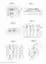
In the traditional wire-bond packaging technique, illustrated in FIG. 1 and 2, an integrated circuit die 10 is placed into a protective package 12 and bond pads 9 of said integrated circuit die 10 are connected to pins 11 of said protective package 12 via tiny bond wires 13. These pins 11 are in turn connected to tracks 14 of a printed circuit board 15.
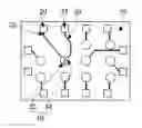
In the more recent flip-chip technique, illustrated in FIG. 3, the integrated circuit die 10 is directly connected to the printed circuit board 15 via solder balls 16 (or solder bumps). In this technique, solder balls 16 are placed onto solder pads 17 of the integrated circuit die 10. Then, the integrated circuit die 10 is flipped and placed onto the printed circuit board 15, the solder balls establishing electrical connections between the solder pads 17 and the tracks 14. As can be seen in FIG. 4, such an integrated circuit die 10 comprises an extra metal layer, called redistribution layer (RDL). The redistribution layer comprises redistribution wires 18 connecting the solder pads 17 to the input/output bond pads 14 of the integrated circuit die 10. As it is classically practiced, a bond pad 20 is dedicated to the digital ground (VSS), and another bond pad 37 is dedicated to test the die 10. Such a test is usually performed by connecting a test circuitry to the dedicated test bond pad 37 of the die 10.
There is a need to prevent a testing of the die after a flip-chip packaging operation while saving a solder ball.
SUMMARY OF THE INVENTION
It is an object of the invention to meet the aforementioned need. Therefore, the invention relates to an electronic system comprising an integrated circuit die, as defined in claim 1.
The integrated circuit die according to the invention behaves differently either there is a solder ball on the split solder pad or not. Such a die may be used for applications in which an integrated circuit die is needed to behave differently before and after an operation of flip-chip packaging. Thus, the split solder pad of the integrated circuit die according to the invention may be used to prevent a testing of the die after a flip-chip packaging operation while saving a solder ball.
As previously mentioned, such a test is usually performed by connecting a test circuitry to a dedicated test bond pad of the die. By using the split solder pad, the test bond pad may be grounded after packaging. This is done by connecting the test bond pad to a first portion of the solder pad and connecting the VSS bond pad to a second portion of the solder pad (c.f. FIG. 5). As long as no solder ball is placed onto the solder pad, the test in enabled. However, when a solder ball connects the first and the second portions, the test bond pad and the VSS bond pads are merged, and the chip can no longer be tested.
In an embodiment, the solder pad is made of two demi-disks.
BRIEF DESCRIPTION OF THE DRAWINGS
Other features and advantages of the present invention will appear more clearly upon reading the following detailed description, made with reference to the annexed drawings given by way of non-limiting examples:
FIG. 1 schematically illustrates a top view of a classical wire-bond package
FIG. 2 schematically illustrates a side view of the package of FIG. 1
FIG. 3 schematically illustrates a side view of a classical flip-chip package
FIG. 4 schematically illustrates an integrated circuit die according to the state of the art
FIG. 5 schematically illustrates an integrated circuit die according to a non-limited embodiment of the invention
FIG. 6 schematically illustrates the integrated circuit die of FIG. 5 used to prevent said die from being tested after a flip-chip packaging.
DETAILED DESCRIPTION OF THE PREFERRED EMBODIMENTS
FIG. 5 shows an integrated circuit die 10′ similar to the integrated circuit die 10 of FIG. 4, with the difference that it comprises a solder pad 19′ that is split in half. More precisely, the solder pad 19′ comprises a first portion 33 and a second portion 34 facing each other, each having a shape of a demi-disk. The first portion 33 is connected to the VSS bond pad 20 via the redistribution wire 22, and the second portion 34 is connected to the test bond pad 37 via the redistribution wire 39.
When no solder ball is placed onto the solder pad 19′, the first portion 33 and the second portion 34 are not in electrical contact with each other. However, when a solder ball is placed onto the solder pad 19′, the first portion 33 and the second portion 34 become in electrical contact with each other. Naturally, the portions 33, 34 may have another shape or be laid out differently on the die 10′, as long as a single solder ball can establish an electrical contact between them.
The key feature of the invention is that the electrical connections between the bond pads linked to the different portions are different depending on whether a solder ball is placed on the solder pad 19′ or not. As a consequence, the split solder pad 19′ may be used in order to prevent the integrated circuit die 10′ from being tested after a flip-chip packaging, as illustrated on FIG. 6. In this example, the VSS bond pad 20 is chip-grounded.
As long as no solder ball is placed onto the solder pad 19′, the die may be tested via the test circuitry 36. In order to do this, one terminal of a resistance 38 is generally connected to the test bond pad 37, and a potential VSS with a high state (“1”) is applied to the other terminal of the resistance 38. As a consequence, the test circuitry 36 is automatically enabled, and the die can be tested. However, after a solder ball 35 is placed onto the solder pad 19′ in order to ground the VSS bond pad 20 via a printed circuit track 24, the test bond pad 37 becomes electrically connected to the VSS bond pad 20, and the test circuitry becomes disabled. This situation is wanted when the integrated circuit die is used in applications (that is to say after packaging), so as to avoid the die to enter a test mode.
Claims
What is claimed is:1. An electronic system comprising:
an integrated circuit die having:
at least 2 bond pads
a redistribution layer, said redistribution layer having:
at least a solder pad comprising 2 portions arranged to enable an electrical connection between each other by a same solder ball placed on said solder pad, but electrically isolated of each other in the absence of a solder ball on the solder pad
at least 2 redistribution wires, each one connecting one of the 2 portions to one of the 2 bond pads, a second bond pad connected via a second redistribution wire to a second portion of the solder pad being dedicated to testing said integrated circuit die
a grounded printed circuit board track, a solder ball being placed between the solder pad and the printed circuit board track.
2. The electronic system according to the previous claim, wherein the portions have a shape of a demi-disk.
Images & Drawings included:
Sources:
- United States Patent and Trademark Office - verify current appl. status at the USPTO↗
Similar patent applications:
- » 20180053738
Integrated circuit die having a split solder pad
Recent applications in this class:
- » 20250293098 2025-09-18
SEMICONDUCTOR DEVICE AND METHOD OF MANUFACTURING THE SAME - » 20250279322 2025-09-04
ELECTRONIC DEVICE, ELECTRONIC STRUCTURE AND METHOD OF MANUFACTURING THE SAME - » 20250266302 2025-08-21
ELECTRONIC DEVICE - » 20250246488 2025-07-31
SUBSTRATE CIRCUIT STRUCTURE - » 20250239495 2025-07-24
SEMICONDUCTOR DIE AND WAFER BONDING CRACK DETECTOR STRUCTURES AND METHODS OF FORMING SAME - » 20250233028 2025-07-17
MICRO-LED WAFER TESTING DEVICE AND MICRO-LED WAFER TESTING METHOD - » 20250226269 2025-07-10
TEST PAD STRUCTURE AND METHOD OF MANUFACTURING AND OPERATING THE SAME - » 20250218876 2025-07-03
STACKED SEMICONDUCTOR DEVICE TEST CIRCUITS AND METHODS OF USE - » 20250218875 2025-07-03
SEMICONDUCTOR DEVICE - » 20250210418 2025-06-26
SEMICONDUCTOR PACKAGE AND PACKAGE MODULE INCLUDING THE SAME
Recent applications for this Assignee:
- » 20250209012 2025-06-26
SYSTEM COMPRISING A PROCESSOR AND PERIPHERALS - » 20250202703 2025-06-19
METHOD FOR VERIFYING THE CONFORMITY OF A NDEF MESSAGE - » 20250175093 2025-05-29
RECTIFIER CIRCUIT FOR AN RFID TAG - » 20250119751 2025-04-10
A BLUETOOTH COMMUNICATION METHOD AND SYSTEM - » 20240403591 2024-12-05
ENERGY HARVESTING WITH DUAL BUFFER CAPACITOR ARRANGEMENT - » 20240348226 2024-10-17
IMPEDANCE MATCHING NETWORK - » 20240211348 2024-06-27
METHOD FOR MANAGING DATA STORED IN A PAGE WITHIN A MEMORY ELEMENT - » 20240211342 2024-06-27
ELECTRONIC DEVICE COMPRISING A BLUETOOTH COMMUNICATION UNIT - » 20240210590 2024-06-27
SKIN CONTACT SENSING DEVICE - » 20240204758 2024-06-20
SYSTEM WITH A LOW-DRIFT ON-CHIP OSCILLATOR WITH LOWERED SENSITIVITY TO RANDOM TELEGRAPH NOISE