Electronic package structure with multiple electronic components
US20180061809A1
2018-03-01
15/352,822
2016-11-16
✅ Patent granted
US 10,573,623 B2
2020-02-25
-
-
Jamie C Niesz | Scott E Bauman
Mintz Levin Cohn Ferris Glovsky and Popeo, P.C. | Peter F. Corless | Steven M. Jensen
2036-11-16
Abstract:
An electronic package structure is provided, which includes: a first carrier having an opening; at least a first electronic component and a plurality of conductive elements disposed on the first carrier; a second carrier bonded to the conductive elements; at least a second electronic component disposed on the second carrier and received in the opening of the first carrier; and an encapsulant formed on the first carrier and the second carrier and encapsulating the first electronic component, the second electronic component and the conductive elements. By receiving the second electronic component in the opening of the first carrier, the present disclosure reduces the height of the electronic package structure. The present disclosure further provides a method for fabricating the electronic package structure.
Assignee:
- Siliconware Precision Industries Co., Ltd. 673 🇹🇼 Taichung, Taiwan
Applicant:
Interested in similar patents?
Get notified when new applications in this technology area are published.
Classification:
H01L25/0657 » CPC main
Assemblies consisting of a plurality of individual semiconductor or other solid state devices ; Multistep manufacturing processes thereof all the devices being of a type provided for in the same subgroup of groups - , e.g. assemblies of rectifier diodes the devices not having separate containers the devices being of a type provided for in group Stacked arrangements of devices
H01L24/17 » CPC further
Arrangements for connecting or disconnecting semiconductor or solid-state bodies; Methods or apparatus related thereto; Means for bonding being attached to, or being formed on, the surface to be connected, e.g. chip-to-package, die-attach, "first-level" interconnects; Manufacturing methods related thereto; Bump connectors ; Manufacturing methods related thereto; Structure, shape, material or disposition of the bump connectors after the connecting process of a plurality of bump connectors
H01L23/49541 » CPC further
Details of semiconductor or other solid state devices; Arrangements for conducting electric current to or from the solid state body in operation, e.g. leads, terminal arrangements ; Selection of materials therefor consisting of soldered constructions; Lead-frames or other flat leads Geometry of the lead-frame
H01L23/3107 » CPC further
Details of semiconductor or other solid state devices; Encapsulations, e.g. encapsulating layers, coatings, e.g. for protection characterised by the arrangement or shape the device being completely enclosed
H01L23/49531 » CPC further
Details of semiconductor or other solid state devices; Arrangements for conducting electric current to or from the solid state body in operation, e.g. leads, terminal arrangements ; Selection of materials therefor consisting of soldered constructions; Lead-frames or other flat leads; Additional leads the additional leads being a wiring board
H01L23/552 » CPC further
Details of semiconductor or other solid state devices Protection against radiation, e.g. light or electromagnetic waves
H01L24/33 » CPC further
Arrangements for connecting or disconnecting semiconductor or solid-state bodies; Methods or apparatus related thereto; Means for bonding being attached to, or being formed on, the surface to be connected, e.g. chip-to-package, die-attach, "first-level" interconnects; Manufacturing methods related thereto; Layer connectors, e.g. plate connectors, solder or adhesive layers; Manufacturing methods related thereto; Structure, shape, material or disposition of the layer connectors after the connecting process of a plurality of layer connectors
H01L24/49 » CPC further
Arrangements for connecting or disconnecting semiconductor or solid-state bodies; Methods or apparatus related thereto; Means for bonding being attached to, or being formed on, the surface to be connected, e.g. chip-to-package, die-attach, "first-level" interconnects; Manufacturing methods related thereto; Wire connectors; Manufacturing methods related thereto; Structure, shape, material or disposition of the wire connectors after the connecting process of a plurality of wire connectors
H01L24/81 » CPC further
Arrangements for connecting or disconnecting semiconductor or solid-state bodies; Methods or apparatus related thereto; Methods for connecting semiconductor or other solid state bodies using means for bonding being attached to, or being formed on, the surface to be connected using a bump connector
H01L25/03 » CPC further
Assemblies consisting of a plurality of individual semiconductor or other solid state devices ; Multistep manufacturing processes thereof all the devices being of a type provided for in the same subgroup of groups - , e.g. assemblies of rectifier diodes
H01L25/105 » CPC further
Assemblies consisting of a plurality of individual semiconductor or other solid state devices ; Multistep manufacturing processes thereof all the devices being of a type provided for in the same subgroup of groups - , e.g. assemblies of rectifier diodes the devices having separate containers the devices being of a type provided for in group
H01L25/16 » CPC further
Assemblies consisting of a plurality of individual semiconductor or other solid state devices ; Multistep manufacturing processes thereof the devices being of types provided for in two or more different main groups of - , e.g. forming hybrid circuits
H01L25/50 » CPC further
Assemblies consisting of a plurality of individual semiconductor or other solid state devices ; Multistep manufacturing processes thereof Multistep manufacturing processes of assemblies consisting of devices, each device being of a type provided for in group or
H01L21/561 » CPC further
Processes or apparatus adapted for the manufacture or treatment of semiconductor or solid state devices or of parts thereof; Manufacture or treatment of semiconductor devices or of parts thereof the devices having at least one potential-jump barrier or surface barrier, e.g. PN junction, depletion layer or carrier concentration layer; Assembly of semiconductor devices using processes or apparatus not provided for in a single one of the subgroups - , e.g. sealing of a cap to a base of a container; Encapsulations, e.g. encapsulation layers, coatings Batch processing
H01L21/568 » CPC further
Processes or apparatus adapted for the manufacture or treatment of semiconductor or solid state devices or of parts thereof; Manufacture or treatment of semiconductor devices or of parts thereof the devices having at least one potential-jump barrier or surface barrier, e.g. PN junction, depletion layer or carrier concentration layer; Assembly of semiconductor devices using processes or apparatus not provided for in a single one of the subgroups - , e.g. sealing of a cap to a base of a container; Encapsulations, e.g. encapsulation layers, coatings Temporary substrate used as encapsulation process aid
H01L23/3128 » CPC further
Details of semiconductor or other solid state devices; Encapsulations, e.g. encapsulating layers, coatings, e.g. for protection characterised by the arrangement or shape the device being completely enclosed a substrate forming part of the encapsulation the substrate having spherical bumps for external connection
H01L2224/0401 » CPC further
Indexing scheme for arrangements for connecting or disconnecting semiconductor or solid-state bodies and methods related thereto as covered by; Means for bonding being attached to, or being formed on, the surface to be connected, e.g. chip-to-package, die-attach, "first-level" interconnects; Manufacturing methods related thereto; Bonding areas; Manufacturing methods related thereto; Structure, shape, material or disposition of the bonding areas prior to the connecting process Bonding areas specifically adapted for bump connectors, e.g. under bump metallisation [UBM]
H01L2225/06517 » CPC further
Details relating to assemblies covered by the group but not provided for in its subgroups; All the devices being of a type provided for in the same subgroup of groups - the devices not having separate containers the devices being of a type provided for in group; Stacked arrangements of devices Bump or bump-like direct electrical connections from device to substrate
H01L2225/06572 » CPC further
Details relating to assemblies covered by the group but not provided for in its subgroups; All the devices being of a type provided for in the same subgroup of groups - the devices not having separate containers the devices being of a type provided for in group; Stacked arrangements of devices Auxiliary carrier between devices, the carrier having an electrical connection structure
H01L2225/1023 » CPC further
Details relating to assemblies covered by the group but not provided for in its subgroups; All the devices being of a type provided for in the same subgroup of groups - the devices having separate containers the devices being of a type provided for in group the containers being in a stacked arrangement the lowermost container comprising a device support the support being an insulating substrate
H01L2225/1058 » CPC further
Details relating to assemblies covered by the group but not provided for in its subgroups; All the devices being of a type provided for in the same subgroup of groups - the devices having separate containers the devices being of a type provided for in group the containers being in a stacked arrangement; Details of electrical connections between containers Bump or bump-like electrical connections, e.g. balls, pillars, posts
H01L2924/00014 » CPC further
Indexing scheme for arrangements or methods for connecting or disconnecting semiconductor or solid-state bodies as covered by; Technical content checked by a classifier the subject-matter covered by the group, the symbol of which is combined with the symbol of this group, being disclosed without further technical details
H01L2924/11 » CPC further
Indexing scheme for arrangements or methods for connecting or disconnecting semiconductor or solid-state bodies as covered by; Details of semiconductor or other solid state devices to be connected Device type
H01L2924/15151 » CPC further
Indexing scheme for arrangements or methods for connecting or disconnecting semiconductor or solid-state bodies as covered by; Details of package parts other than the semiconductor or other solid state devices to be connected; Die mounting substrate; Shape the die mounting substrate comprising an aperture, e.g. for underfilling, outgassing, window type wire connections
H01L2924/15311 » CPC further
Indexing scheme for arrangements or methods for connecting or disconnecting semiconductor or solid-state bodies as covered by; Details of package parts other than the semiconductor or other solid state devices to be connected; Die mounting substrate; Connection portion the connection portion being formed only on the surface of the substrate opposite to the die mounting surface being a ball array, e.g. BGA
H01L2924/15321 » CPC further
Indexing scheme for arrangements or methods for connecting or disconnecting semiconductor or solid-state bodies as covered by; Details of package parts other than the semiconductor or other solid state devices to be connected; Die mounting substrate; Connection portion the connection portion being formed on the die mounting surface of the substrate being a ball array, e.g. BGA
H01L2924/181 » CPC further
Indexing scheme for arrangements or methods for connecting or disconnecting semiconductor or solid-state bodies as covered by; Details of package parts other than the semiconductor or other solid state devices to be connected Encapsulation
H01L2924/19041 » CPC further
Indexing scheme for arrangements or methods for connecting or disconnecting semiconductor or solid-state bodies as covered by; Details of hybrid assemblies other than the semiconductor or other solid state devices to be connected; Structure; Component type being a capacitor
H01L2924/19042 » CPC further
Indexing scheme for arrangements or methods for connecting or disconnecting semiconductor or solid-state bodies as covered by; Details of hybrid assemblies other than the semiconductor or other solid state devices to be connected; Structure; Component type being an inductor
H01L2924/19043 » CPC further
Indexing scheme for arrangements or methods for connecting or disconnecting semiconductor or solid-state bodies as covered by; Details of hybrid assemblies other than the semiconductor or other solid state devices to be connected; Structure; Component type being a resistor
H01L2924/19105 » CPC further
Indexing scheme for arrangements or methods for connecting or disconnecting semiconductor or solid-state bodies as covered by; Details of hybrid assemblies other than the semiconductor or other solid state devices to be connected; Disposition of discrete passive components in a side-by-side arrangement on a common die mounting substrate
H01L2924/19106 » CPC further
Indexing scheme for arrangements or methods for connecting or disconnecting semiconductor or solid-state bodies as covered by; Details of hybrid assemblies other than the semiconductor or other solid state devices to be connected; Disposition of discrete passive components in a mirrored arrangement on two different side of a common die mounting substrate
H01L2924/19107 » CPC further
Indexing scheme for arrangements or methods for connecting or disconnecting semiconductor or solid-state bodies as covered by; Details of hybrid assemblies other than the semiconductor or other solid state devices to be connected; Disposition of discrete passive components off-chip wires
H01L2924/3025 » CPC further
Indexing scheme for arrangements or methods for connecting or disconnecting semiconductor or solid-state bodies as covered by; Technical effects; Electrical effects Electromagnetic shielding
H01L25/065 IPC
Assemblies consisting of a plurality of individual semiconductor or other solid state devices ; Multistep manufacturing processes thereof all the devices being of a type provided for in the same subgroup of groups - , e.g. assemblies of rectifier diodes the devices not having separate containers the devices being of a type provided for in group
H01L25/10 IPC
Assemblies consisting of a plurality of individual semiconductor or other solid state devices ; Multistep manufacturing processes thereof all the devices being of a type provided for in the same subgroup of groups - , e.g. assemblies of rectifier diodes the devices having separate containers
H01L23/495 IPC
Details of semiconductor or other solid state devices; Arrangements for conducting electric current to or from the solid state body in operation, e.g. leads, terminal arrangements ; Selection of materials therefor consisting of soldered constructions Lead-frames or other flat leads
H01L21/56 » CPC further
Processes or apparatus adapted for the manufacture or treatment of semiconductor or solid state devices or of parts thereof; Manufacture or treatment of semiconductor devices or of parts thereof the devices having at least one potential-jump barrier or surface barrier, e.g. PN junction, depletion layer or carrier concentration layer; Assembly of semiconductor devices using processes or apparatus not provided for in a single one of the subgroups - , e.g. sealing of a cap to a base of a container Encapsulations, e.g. encapsulation layers, coatings
H01L23/31 IPC
Details of semiconductor or other solid state devices; Encapsulations, e.g. encapsulating layers, coatings, e.g. for protection characterised by the arrangement or shape
H01L23/00 IPC
Details of semiconductor or other solid state devices
H01L25/00 IPC
Assemblies consisting of a plurality of individual semiconductor or other solid state devices ; Multistep manufacturing processes thereof
Description
BACKGROUND
1. Technical Field
The present disclosure relates to package structures, and, more particularly, to a stack-type electronic package structure and a method of fabricating the same.
2. Description of Related Art
Along with the rapid development of portable electronic products, modern products have been developed toward the trend of high density, high performance and miniaturization. Accordingly, various package on package (PoP) technologies are developed in semiconductor packaging industries to meet the requirements of high density and miniaturization.
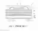
FIG. 1 is a schematic cross-sectional view of a conventional PoP structure 1. Referring to FIG. 1, the PoP structure 1 has: a first substrate 10 having a first surface 10a and a second surface 10b opposite to the first surface 10a; a first semiconductor chip 11 disposed on the first surface 10a of the first substrate 10; a plurality of solder posts 13 disposed on the first surface 10a of the first substrate 10; a first encapsulant 16 formed on the first surface 10a of the first substrate 10 to encapsulate the first semiconductor chip 11 and the solder posts 13; a plurality of solder balls 15 formed on the second surface 10b of the first substrate 10; a second substrate 14 stacked on the first substrate 10 through the solder posts 13; a plurality of second semiconductor chips 12 wire-bonded to the second substrate 14; and a second encapsulant 17 formed on the second substrate 14 to encapsulate the second semiconductor chips 12.
Generally, there is no more space available for passive components to be added to the PoP structure 1, and the electrical performance of the PoP structure 1 cannot be further optimized Besides, passive components are generally higher than the first semiconductor chip 11 and the second semiconductor chips 12. As such, if a passive component is added, the height of the PoP structure 1 will be greatly increased. For example, if the passive component is disposed on the first substrate 10, the height of the solder posts 13 will be increased; otherwise, if the passive component is disposed on the second substrate 14, the height of the second encapsulant 17 will be increased. Consequently, the PoP structure 1 cannot meet the miniaturization requirement.
Therefore, there is a need to provide an electronic package structure and a fabrication method thereof so as to overcome the above-described drawbacks.
SUMMARY
In view of the above-described drawbacks, the present disclosure provides an electronic package structure, which comprises: a first carrier having an opening; at least a first electronic component disposed on and electrically connected to the first carrier; a plurality of conductive elements disposed on and electrically connected to the first carrier;
a second carrier bonded to the conductive elements and electrically connected to the first carrier; at least a second electronic component disposed on the second carrier and received in the opening of the first carrier; and a first encapsulant formed on the second carrier and encapsulating the second electronic component and the conductive elements.
The present disclosure further provides a method for fabricating an electronic package structure, which comprises: providing a first carrier having an opening with at least a first electronic component disposed on and electrically connected to the first carrier; bonding and electrically connecting the first carrier to a second carrier through a plurality of conductive elements with at least a second electronic component disposed on the second carrier and received in the opening of the first carrier; and forming on the second carrier a first encapsulant encapsulating the second electronic component and the conductive elements.
In an embodiment, the first encapsulant is further formed on the first carrier and encapsulates the first electronic component.
In an embodiment, the opening is positioned within an edge of the first carrier.
In an embodiment, the opening is positioned on a side of the first carrier.
In an embodiment, the opening is positioned on a corner of the first carrier.
In an embodiment, at least one of the first electronic component and the second electronic component is a package, an active component, or a passive component.
In an embodiment, the conductive elements are solder balls, copper core balls, metal elements, circuit boards, or any combination thereof.
In an embodiment, at least one of the first carrier and the second carrier is a circuit structure, a lead frame, a wafer, or a carrier board with a metal layout.
In an embodiment, the first electronic component is positioned between the first carrier and the second carrier.
In an embodiment, the second electronic component is electrically connected to the first carrier, the second carrier or both the first and second carriers.
In an embodiment, the second electronic component is electrically connected to the first carrier through a conductor.
In an embodiment, the second carrier has at least a board served as an EMI shield.
In an embodiment, before formation of the encapsulant, a second encapsulant is formed and encapsulates the first electronic component.
Therefore, by receiving the second electronic component such as a passive component in the opening of the first carrier, the present disclosure reduces the height of the electronic package structure so as to meet the miniaturization requirement.
BRIEF DESCRIPTION OF DRAWINGS
FIG. 1 is a schematic cross-sectional view of a conventional PoP structure;
FIGS. 2A to 2C are schematic cross-sectional views showing a method for fabricating an electronic package structure according to a first embodiment of the present disclosure, wherein FIG. 2B′ shows another embodiment of FIG. 2B, and FIGS. 2C′ and 2C″ show other embodiments of FIG. 2C;
FIGS. 3A to 3D are schematic upper views showing various aspects of a first carrier of FIG. 2A;
FIG. 4 is a schematic cross-sectional view of an electronic package structure according to a second embodiment of the present disclosure; and
FIGS. 5A and 5B are schematic cross-sectional views showing various aspects of FIG. 2C′.
DETAILED DESCRIPTION OF EMBODIMENTS
The following illustrative embodiments are provided to illustrate the disclosure of the present disclosure, these and other advantages and effects can be apparent to those in the art after reading this specification.
It should be noted that all the drawings are not intended to limit the present disclosure. Various modifications and variations can be made without departing from the spirit of the present disclosure. Further, terms such as “first”, “second”, “on”, “a” etc. are merely for illustrative purposes and should not be construed to limit the scope of the present disclosure.
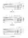
FIGS. 2A to 2C are schematic cross-sectional views showing a method for fabricating an electronic package structure 2 according to a first embodiment of the present disclosure.
Referring to FIG. 2A, a first carrier 20 is provided. The first carrier 20 has a first side 20a, a second side 20b opposite to the first side 20a, and at least an opening 201 communicating the first side 20a and the second side 20b. At least a first electronic component 21 and a plurality of conductive elements 23 such as solder balls are disposed on the first side 20a of the first carrier 20, and a plurality of first electronic components 21′, 21″ are disposed on the second side 20b of the first carrier 20.
In an embodiment, the first carrier 20 is a core circuit structure such as a packaging substrate, or a coreless circuit structure, and has a plurality of circuit layers 200 such as fan-out redistribution layers. In another embodiment, the first carrier 20 is a lead frame, a wafer, or a carrier board with a metal layout (for example, low temperature cofired ceramic (LTCC) or ferrite).
The number of the opening 201 can be one or more, and the position thereof can be determined according to the practical need and varied corresponding to the arrangement of the circuit layers 200. In an embodiment, the opening 201 can be positioned at a center, a periphery or a corner of the first carrier 20 so as to increase the area utilization of the first carrier 20. FIGS. 3A to 3D are schematic upper views showing various aspects of the first carrier 20. Referring to FIG. 3A, the opening 201 is completely positioned within an edge 20c of the first carrier 20. Referring to FIG. 3B, one side of the opening 201 communicates with an edge 20c of the first carrier 20, i.e., a side of the first carrier 20. Referring to FIG. 3C, two sides of the opening 201 communicate with an edge 20c of the first carrier 20, that is, the opening 201 is positioned on a corner of the first carrier 20. Referring to FIG. 3D, three sides of the opening 201 communicate with an edge 20c of the first carrier 20, that is, a side portion of the first carrier 20 is removed.
In an embodiment, at least one of the first electronic components 21, 21′, 21″ is a package such as a chip scale package, an active component such as a semiconductor chip, a passive component, such as a resistor, a capacitor or an inductor, or a combination thereof. In an embodiment, the first electronic component 21 is an active component, the first electronic component 21′ is a package, and the first electronic component 21″ is a passive component. In an embodiment, the first electronic components 21, 21′ are disposed in a flip-chip manner on and electrically connected to the circuit layers 200 through a plurality of conductive bumps 210. In an embodiment, the conductive bumps 210 are made of such as a solder material. In another embodiment, the first electronic components 21, 21′ are electrically connected to the circuit layers 200 through bonding wires (not shown). In another embodiment, the first electronic component 21″ is in direct contact with the circuit layers 200.
A second carrier 24 having at least a second electronic component 22 disposed thereon is provided. In an embodiment, the second carrier 24 is a lead frame having a plurality of conductive pads 240, 240′ that are separated from one another. The second electronic component 22 is bonded to the conductive pads 240′ so as to be electrically connected to the second carrier 24. In another embodiment, the second carrier 24 is a carrier carrying chips. In an embodiment, the second carrier 24 is a core circuit structure, a coreless circuit structure, a wafer, or a carrier board with a metal layout (such as LTCC or ferrite).
The second carrier 24 is optionally disposed on a supporting member 25 such as a tape. In an embodiment, the second electronic component 22 is a package such as a chip scale package, an active component such as a semiconductor chip, a passive component, such as a resistor, a capacitor or an inductor, or a combination thereof. In an embodiment, the second electronic component 22 is a passive component.
Referring to FIG. 2B, the first carrier 20 is bonded to the conductive pads 240 of the second carrier 24 through the conductive elements 23. As such, the circuit layers 200 of the first carrier 20 are electrically connected to the second carrier 24 and the second electronic component 22 is received in the opening 201 of the first carrier 20.
In another embodiment, referring to FIG. 2B′, the first carrier 20 is stacked on the second carrier 24 first and then the second electronic component 22 is disposed on the conductive pads 240′ of the second carrier 24 and received in the opening 201 of the first carrier 20.
Referring to FIG. 2C, a first encapsulant 26 is formed on the first carrier 20 and the second carrier 24 (or the supporting member 25) and filled in the opening 201 so as to encapsulate the first electronic components 21, 21′, 21″, the second electronic component 22 and the conductive elements 23. Thereafter, the supporting member 25 is removed.
In an embodiment, the first encapsulant 26 is made of polyimide, a dry film, an epoxy resin, or a molding compound. The first encapsulant 26 has a first surface 26a and a second surface 26b opposite to the first surface 26a. The second carrier 24 is embedded in the first surface 26a of the first encapsulant 26, and the conductive pads 240 are exposed from the first surface 26a of the first encapsulant 26. In an embodiment, surfaces of the conductive pads 240 are flush with the first surface 26a of the first encapsulant 26. As such, a solder material such as solder balls (not shown) can further be formed on the exposed surfaces of the conductive pads 240 for bonding with an electronic device such as a circuit board.
Further, referring to FIG. 2C′, the conductive elements 23′ can be ring-shaped circuit boards or strip-shaped circuit boards that are bonded to the circuit layers 200 and the conductive pads 240 through a solder material 23a, thus increasing the gap between the first carrier 20 and the second carrier 24 and providing sufficient space between the first and second carrier 20, 24 for receiving the first electronic component 21. In another embodiment, referring to FIG. 2C″, the conductive elements 23″ are copper core balls or (post-shaped, block-shaped or pin-shaped) metal elements of copper or gold.
Again referring to FIG. 2C′, the second electronic component 22 is electrically connected to the circuit layers 200 of the first carrier 20 of the first carrier 20 through conductors 220 such as bonding wires or clip bars. In another embodiment, referring to FIG. 5A, the conductors 220 electrically connect the circuit layers 200 of the first carrier 20 and circuits 540 of the second carrier 24. The circuits 540 are electrically connected to the conductive pads 240′. In a further embodiment, referring to FIG. 5B, the conductors 220 electrically connect side circuits 500 of the first carrier 20 and the second electronic component 22. In an embodiment, the conductors 220 are made of a conductive adhesive or a solder material.
Again referring to FIG. 2C″, the second carrier 24′ further has at least a board 241 that can be separated from or connected to the conductive pads 240, 240′ and grounded to provide an electromagnetic interference (EMI) shielding effect.
Therefore, since the second electronic component 22 (such as a passive component) disposed on the second carrier 24 is received in the opening 201 of the first carrier 20, the present disclosure reduces the height of the electronic package structure 2 and meets the miniaturization requirement.
Further, the second carrier 24′ provides an EMI shielding effect. In addition, if the second carrier 24, 24′ is a lead frame or a metal board, the heat dissipating efficiency of the electronic package structure 2 is improved.
Conventionally, active components and passive components are disposed on the same substrate and electrically connected through circuits of the substrate. By contrast, according to the present disclosure the second electronic component 22 (passive component) and the first electronic component 21 (active component) of the electronic package structure 2 are disposed on different carriers and cannot be directly electrically connected through circuits of the same carrier. Through the design of the conductors 220, the present disclosure reduces the wiring area of the first carrier 20 and the second carrier 24 (for example, the I/O count) and reduces AC and DC impedances. Referring to FIG. 2C, if the first electronic component 21 is electrically through the conductive elements 23, the conductive pads 240, and circuits (not shown) of the second carrier 24 to the conductive pads 240′ and the second electronic component 22, the circuits between the conductive pads 240, 240′ will be longer than the circuits 540 of FIG. 5A.
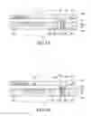
FIG. 4 is a schematic cross-sectional view of an electronic package structure 4 according to a second embodiment of the present disclosure.
Referring to FIG. 4, before the process of FIG. 2B is performed, a second encapsulant 47 is formed on the second side 20b of the first carrier 20 to encapsulate the first electronic components 21′, 21″. The second encapsulant 47 is not filled in the opening 201. Then, the processes of FIGS. 2B to 2C are performed to obtain the electronic package structure 4.
In an embodiment, the second encapsulant 47 is made of polyimide, a dry film, an epoxy resin or a molding compound. The first encapsulant 26 and the second encapsulant 47 can be made of the same or different materials.
Through the above-described processes, the present disclosure further provides an electronic package structure 2, 4, which has: a first carrier 20 having at least an opening 201; a plurality of first electronic components 21, 21′, 21″ and a plurality of conductive elements 23, 23′, 23″ disposed on and electrically connected to the first carrier 20; a second carrier 24, 24′ bonded to the conductive elements 23 so as to be electrically connected to the first carrier 20; at least a second electronic component 22 disposed on the second carrier 24, 24′ and received in the opening 201; and a first encapsulant 26 formed on the first carrier 20 and the second carrier 24, 24′ and encapsulating the first electronic component 21 (and the first electronic components 21′, 21″), the second electronic component 22 and the conductive elements 23, 23′, 23″.
In an embodiment, the opening 201 is positioned within an edge 20c of the first carrier 20.
In an embodiment, the opening 201 is positioned on a side of the first carrier 20.
In an embodiment, the opening 201 is positioned on a corner of the first carrier 20.
In an embodiment, at least one of the first electronic components 21, 21′, 21″ and the second electronic component 22 is a package, an active component, a passive component, or a combination thereof.
In an embodiment, the conductive elements 23, 23′, 23″ are solder balls, copper core balls, metal elements or circuit boards.
In an embodiment, at least one of the first carrier 20 and the second carrier 24, 24′ is a circuit structure, a lead frame, a wafer, or a carrier board with a metal layout.
In an embodiment, the first electronic component 21 is positioned between the first carrier 20 and the second carrier 24.
In an embodiment, the second electronic component 22 is electrically connected to at least one of the first carrier 20 and the second carrier 24, 24′.
In an embodiment, the second electronic component 22 is electrically connected to the first carrier 20 through conductors 220.
In an embodiment, the second carrier 24′ has at least a board 241 served as an EMI shield.
In an embodiment, the electronic package structure 4 further has a second encapsulant 47 encapsulating the first electronic components 21′, 21″.
Therefore, by receiving the second electronic component such as a passive component in the opening of the first carrier, the present disclosure reduces the height of the electronic package structure so as to meet the miniaturization requirement.
Further, the second carrier provides an EMI shielding effect and improves the heat dissipating efficiency of the electronic package structure.
The above-described descriptions of the detailed embodiments are only to illustrate the implementation according to the present disclosure, and it is not to limit the scope of the present disclosure. Accordingly, all modifications and variations completed by those with ordinary skill in the art should fall within the scope of present disclosure defined by the appended claims
Claims
1. An electronic package structure, comprising:
a first carrier having an opening;
at least a first electronic component disposed on and electrically connected to the first carrier;
a plurality of conductive elements disposed on and electrically connected to the first carrier;
a second carrier bonded to the conductive elements and electrically connected to the first carrier;
at least a second electronic component received in the opening of the first carrier and disposed on the second carrier, wherein a height of the second electronic component is greater than a distance between the first carrier and the second carrier; and
a first encapsulant formed on the second carrier and encapsulating the second electronic component and the conductive elements.
2. The electronic package structure of claim 1, wherein the first encapsulant is further formed on the first carrier and encapsulates the first electronic component.
3. The electronic package structure of claim 1, wherein the opening is positioned within an edge of the first carrier, on a side of the first carrier, or on a corner of the first carrier.
4. The electronic package structure of claim 1, wherein at least one of the first electronic component and the second electronic component is a package, an active component, or a passive component.
5. The electronic package structure of claim 1, wherein the conductive elements are solder balls, copper core balls, metal elements, circuit boards, or any combination thereof.
6. The electronic package structure of claim 1, wherein at least one of the first carrier and the second carrier is a circuit structure, a lead frame, a wafer, or a carrier board with a metal layout.
7. The electronic package structure of claim 1, wherein the first electronic component is positioned between the first carrier and the second carrier, and the second electronic component is electrically connected to at least one of the first carrier and the second carrier.
8. The electronic package structure of claim 7, further comprising a conductor electrically connecting the second electronic component to the first carrier.
9. The electronic package structure of claim 1, wherein the second carrier has at least a board served as an electromagnetic interference (EMI) shield.
10. The electronic package structure of claim 1, further comprising a second encapsulant encapsulating the first electronic component.
11. A method for fabricating an electronic package structure, comprising:
providing a first carrier having an opening with at least a first electronic component disposed on and electrically connected to the first carrier;
bonding and electrically connecting the first carrier to a second carrier through a plurality of conductive elements with at least a second electronic component received in the opening of the first carrier and disposed on the second carrier; and
forming on the second carrier a first encapsulant encapsulating the second electronic component and the conductive elements.
12. The method of claim 11, wherein the first encapsulant is further formed on the first carrier and encapsulates the first electronic component.
13. The method of claim 11, wherein the opening is positioned within an edge of the first carrier, on a side of the first carrier, or on a corner of the first carrier.
14. The method of claim 11, wherein at least one of the first electronic component and the second electronic component is a package, an active component, or a passive component.
15. The method of claim 11, wherein the conductive elements are solder balls, copper core balls, metal elements, circuit boards, or any combination thereof.
16. The method of claim 11, wherein at least one of the first carrier and the second carrier is a circuit structure, a lead frame, a wafer, or a carrier board with a metal layout.
17. The method of claim 11, wherein the first electronic component is positioned between the first carrier and the second carrier, and the second electronic component is electrically connected to at least one of the first carrier and the second carrier.
18. The method of claim 17, further comprising providing a conductor electrically connecting the second electronic component to the first carrier.
19. The method of claim 11, wherein the second carrier has at least a board served an electromagnetic interference (EMI) shield.
20. The method of claim 11, further comprising, prior to forming the first encapsulant, forming a second encapsulant encapsulating the first electronic component.
Images & Drawings included:


Sources:
- United States Patent and Trademark Office - verify current appl. status at the USPTO↗
Similar patent applications:
Recent applications in this class:
- » 20250293212 2025-09-18
SEMICONDUCTOR PACKAGES - » 20250293211 2025-09-18
HEAT DISSIPATION FOR STACKED INTEGRATED CIRCUIT DEVICES - » 20250293210 2025-09-18
SYSTEMS AND METHODS FOR PACKAGING A SEMICONDUCTOR DEVICE - » 20250286021 2025-09-11
SEMICONDUCTOR PACKAGE - » 20250286020 2025-09-11
SEMICONDUCTOR BONDING STRUCTURE - » 20250286019 2025-09-11
SEMICONDUCTOR PACKAGE - » 20250286018 2025-09-11
METHOD OF FABRICATING SEMICONDUCTOR BONDING STRUCTURE - » 20250286017 2025-09-11
SEMICONDUCTOR DEVICE - » 20250279399 2025-09-04
SEMICONDUCTOR DEVICES AND MANUFACTURING METHODS OF THE SAME - » 20250279398 2025-09-04
VERTICAL INTERCONNECT STRUCTURES IN THREE-DIMENSIONAL INTEGRATED CIRCUITS
Recent applications for this Assignee:
- » 20250046771 2025-02-06
METHOD FOR FABRICATING ELECTRONIC PACKAGE - » 20250015054 2025-01-09
CARRYING SUBSTRATE, ELECTRONIC PACKAGE HAVING THE CARRYING SUBSTRATE, AND METHODS FOR MANUFACTURING THE SAME - » 20240379534 2024-11-14
ELECTRONIC PACKAGE, MANUFACTURING METHOD FOR THE SAME, AND ELECTRONIC STRUCTURE - » 20240321798 2024-09-26
Electronic package and carrier thereof and method for manufacturing the same - » 20240321784 2024-09-26
Electronic package including lead frame having multiple conductive posts - » 20240321591 2024-09-26
METHOD FOR FABRICATING ELECTRONIC PACKAGE - » 20240290701 2024-08-29
ELECTRONIC PACKAGE AND MANUFACTURING METHOD THEREOF - » 20240290675 2024-08-29
Electronic package and manufacturing method thereof - » 20240290674 2024-08-29
ELECTRONIC PACKAGE AND MANUFACTURING METHOD THEREOF - » 20240282674 2024-08-22
ELECTRONIC PACKAGE AND METHOD OF FABRICATING THE SAME