Semiconductor device having a plurality of semiconductor modules connected by a connection component
US20180130748A1
2018-05-10
15/788,148
2017-10-19
✅ Patent granted
US 10,304,777 B2
2019-05-28
-
-
Ngan V Ngo
Oliff PLC
2037-10-19
Abstract:
A semiconductor device includes an assembly configured such that a plurality of semiconductor modules is connected by a component. Each of the plurality of semiconductor modules includes a semiconductor element including a front-surface electrode fixing a front-surface electrode plate and a back-surface electrode fixing a back-surface electrode plate, wherein the component is either of a first component and a second component. The first component being configured to connect adjacent semiconductor modules to each other such that a front-surface electrode plate of one of the adjacent semiconductor modules is connected to a back-surface electrode plate of the other one of the adjacent semiconductor modules. The second component is configured to connect adjacent semiconductor modules such that respective front-surface electrode plates are connected and respective back-surface electrode plates are connected. The semiconductor modules are connected by the first component or the second component.
Inventors:
- Tomomi OKUMURA 6 🇯🇵 Kariya-shi, Japan
- Takashi UETA 1 🇯🇵 Toyota-shi, Japan
- Tomomi Okumura 10 🇯🇵 Kariya, Japan
- Takashi Ueta 1 🇯🇵 Toyota, Japan
Assignee:
- TOYOTA JIDOSHA KABUSHIKI KAISHA 25,166 🇯🇵 Toyota-shi, Japan
- TOYOTA JIDOSHA KABUSHIKI KAISHA 14,880 🇯🇵 Toyota, Japan
Applicant:
Interested in similar patents?
Get notified when new applications in this technology area are published.
Classification:
H01L23/5386 » CPC main
Details of semiconductor or other solid state devices; Arrangements for conducting electric current within the device in operation from one component to another, i.e. interconnections, e.g. wires, lead frames the interconnection structure between a plurality of semiconductor chips being formed on, or in, insulating substrates Geometry or layout of the interconnection structure
H01L27/06 IPC
Devices consisting of a plurality of semiconductor or other solid-state components formed in or on a common substrate including semiconductor components specially adapted for rectifying, oscillating, amplifying or switching and having at least one potential-jump barrier or surface barrier; including integrated passive circuit elements with at least one potential-jump barrier or surface barrier the substrate being a semiconductor body including a plurality of individual components in a non-repetitive configuration
H01L23/3107 » CPC further
Details of semiconductor or other solid state devices; Encapsulations, e.g. encapsulating layers, coatings, e.g. for protection characterised by the arrangement or shape the device being completely enclosed
H01L2924/183 » CPC further
Indexing scheme for arrangements or methods for connecting or disconnecting semiconductor or solid-state bodies as covered by; Details of package parts other than the semiconductor or other solid state devices to be connected; Encapsulation Connection portion, e.g. seal
H01L23/3185 » CPC further
Details of semiconductor or other solid state devices; Encapsulations, e.g. encapsulating layers, coatings, e.g. for protection characterised by the arrangement or shape; Partial encapsulation or coating the coating covering also the sidewalls of the semiconductor body
H01L23/4334 » CPC further
Details of semiconductor or other solid state devices; Arrangements for cooling, heating, ventilating or temperature compensation ; Temperature sensing arrangements; Fillings or auxiliary members in containers or encapsulations selected or arranged to facilitate heating or cooling; Auxiliary members in containers characterised by their shape, e.g. pistons Auxiliary members in encapsulations
H01L23/4922 » CPC further
Details of semiconductor or other solid state devices; Arrangements for conducting electric current to or from the solid state body in operation, e.g. leads, terminal arrangements ; Selection of materials therefor consisting of soldered constructions; Bases or plates or solder therefor having a heterogeneous or anisotropic structure
H01L23/49517 » CPC further
Details of semiconductor or other solid state devices; Arrangements for conducting electric current to or from the solid state body in operation, e.g. leads, terminal arrangements ; Selection of materials therefor consisting of soldered constructions; Lead-frames or other flat leads Additional leads
H01L23/49537 » CPC further
Details of semiconductor or other solid state devices; Arrangements for conducting electric current to or from the solid state body in operation, e.g. leads, terminal arrangements ; Selection of materials therefor consisting of soldered constructions; Lead-frames or other flat leads Plurality of lead frames mounted in one device
H01L23/49541 » CPC further
Details of semiconductor or other solid state devices; Arrangements for conducting electric current to or from the solid state body in operation, e.g. leads, terminal arrangements ; Selection of materials therefor consisting of soldered constructions; Lead-frames or other flat leads Geometry of the lead-frame
H01L23/49562 » CPC further
Details of semiconductor or other solid state devices; Arrangements for conducting electric current to or from the solid state body in operation, e.g. leads, terminal arrangements ; Selection of materials therefor consisting of soldered constructions; Lead-frames or other flat leads; Geometry of the lead-frame for devices being provided for in
H01L23/49575 » CPC further
Details of semiconductor or other solid state devices; Arrangements for conducting electric current to or from the solid state body in operation, e.g. leads, terminal arrangements ; Selection of materials therefor consisting of soldered constructions; Lead-frames or other flat leads Assemblies of semiconductor devices on lead frames
H01L24/30 » CPC further
Arrangements for connecting or disconnecting semiconductor or solid-state bodies; Methods or apparatus related thereto; Means for bonding being attached to, or being formed on, the surface to be connected, e.g. chip-to-package, die-attach, "first-level" interconnects; Manufacturing methods related thereto; Layer connectors, e.g. plate connectors, solder or adhesive layers; Manufacturing methods related thereto; Structure, shape, material or disposition of the layer connectors prior to the connecting process of a plurality of layer connectors
H01L24/83 » CPC further
Arrangements for connecting or disconnecting semiconductor or solid-state bodies; Methods or apparatus related thereto; Methods for connecting semiconductor or other solid state bodies using means for bonding being attached to, or being formed on, the surface to be connected using a layer connector
H01L25/072 » CPC further
Assemblies consisting of a plurality of individual semiconductor or other solid state devices ; Multistep manufacturing processes thereof all the devices being of a type provided for in the same subgroup of groups - , e.g. assemblies of rectifier diodes the devices not having separate containers the devices being of a type provided for in group the devices being arranged next to each other
H01L25/18 » CPC further
Assemblies consisting of a plurality of individual semiconductor or other solid state devices ; Multistep manufacturing processes thereof the devices being of types provided for in two or more different subgroups of the same main group of groups -
H01L27/0629 » CPC further
Devices consisting of a plurality of semiconductor or other solid-state components formed in or on a common substrate including semiconductor components specially adapted for rectifying, oscillating, amplifying or switching and having at least one potential-jump barrier or surface barrier; including integrated passive circuit elements with at least one potential-jump barrier or surface barrier the substrate being a semiconductor body including a plurality of individual components in a non-repetitive configuration integrated circuits having a two-dimensional layout of components without a common active region comprising components of the field-effect type in combination with diodes, or resistors, or capacitors
H01L23/31 IPC
Details of semiconductor or other solid state devices; Encapsulations, e.g. encapsulating layers, coatings, e.g. for protection characterised by the arrangement or shape
H01L25/07 IPC
Assemblies consisting of a plurality of individual semiconductor or other solid state devices ; Multistep manufacturing processes thereof all the devices being of a type provided for in the same subgroup of groups - , e.g. assemblies of rectifier diodes the devices not having separate containers the devices being of a type provided for in group
H01L25/10 IPC
Assemblies consisting of a plurality of individual semiconductor or other solid state devices ; Multistep manufacturing processes thereof all the devices being of a type provided for in the same subgroup of groups - , e.g. assemblies of rectifier diodes the devices having separate containers
H01L25/11 » CPC further
Assemblies consisting of a plurality of individual semiconductor or other solid state devices ; Multistep manufacturing processes thereof all the devices being of a type provided for in the same subgroup of groups - , e.g. assemblies of rectifier diodes the devices having separate containers the devices being of a type provided for in group
H01L23/433 IPC
Details of semiconductor or other solid state devices; Arrangements for cooling, heating, ventilating or temperature compensation ; Temperature sensing arrangements; Fillings or auxiliary members in containers or encapsulations selected or arranged to facilitate heating or cooling Auxiliary members in containers characterised by their shape, e.g. pistons
H01L23/492 IPC
Details of semiconductor or other solid state devices; Arrangements for conducting electric current to or from the solid state body in operation, e.g. leads, terminal arrangements ; Selection of materials therefor consisting of soldered constructions Bases or plates or solder therefor
H01L23/495 IPC
Details of semiconductor or other solid state devices; Arrangements for conducting electric current to or from the solid state body in operation, e.g. leads, terminal arrangements ; Selection of materials therefor consisting of soldered constructions Lead-frames or other flat leads
H01L23/538 IPC
Details of semiconductor or other solid state devices; Arrangements for conducting electric current within the device in operation from one component to another, i.e. interconnections, e.g. wires, lead frames the interconnection structure between a plurality of semiconductor chips being formed on, or in, insulating substrates
H01L29/739 IPC
Semiconductor devices adapted for rectifying, amplifying, oscillating or switching, or capacitors or resistors with at least one potential-jump barrier or surface barrier, e.g. PN junction depletion layer or carrier concentration layer; Details of semiconductor bodies or of electrodes thereof; Multistep manufacturing processes therefor; Types of semiconductor device ; Multistep manufacturing processes therefor controllable by only the electric current supplied, or only the electric potential applied, to an electrode which does not carry the current to be rectified, amplified or switched; Bipolar devices; Transistor-type devices, i.e. able to continuously respond to applied control signals controlled by field-effect, e.g. bipolar static induction transistors [BSIT]
H01L25/105 » CPC further
Assemblies consisting of a plurality of individual semiconductor or other solid state devices ; Multistep manufacturing processes thereof all the devices being of a type provided for in the same subgroup of groups - , e.g. assemblies of rectifier diodes the devices having separate containers the devices being of a type provided for in group
H01L29/861 » CPC further
Semiconductor devices adapted for rectifying, amplifying, oscillating or switching, or capacitors or resistors with at least one potential-jump barrier or surface barrier, e.g. PN junction depletion layer or carrier concentration layer; Details of semiconductor bodies or of electrodes thereof; Multistep manufacturing processes therefor; Types of semiconductor device ; Multistep manufacturing processes therefor controllable only by variation of the electric current supplied, or only the electric potential applied, to one or more of the electrodes carrying the current to be rectified, amplified, oscillated or switched Diodes
H01L23/4952 » CPC further
Details of semiconductor or other solid state devices; Arrangements for conducting electric current to or from the solid state body in operation, e.g. leads, terminal arrangements ; Selection of materials therefor consisting of soldered constructions; Lead-frames or other flat leads; Additional leads the additional leads being a bump or a wire
H01L23/00 IPC
Details of semiconductor or other solid state devices
Description
INCORPORATION BY REFERENCE
The disclosure of Japanese Patent Application No. 2016-218775 filed on Nov. 9, 2016 including the specification, drawings and abstract is incorporated herein by reference in its entirety.
BACKGROUND
1. Technical Field
The present specification discloses a semiconductor device in which a plurality of semiconductor elements is sealed in a molding resin in an integrated manner.
2. Description of Related Art
Japanese Patent Application Publication No. 2012-235081 (JP 2012-235081 A) discloses semiconductor devices in which two semiconductor elements are sealed in a molding resin in an integrated manner, i.e., a semiconductor device in which two semiconductor elements are connected in series in a molding resin, and a semiconductor device in which two semiconductor elements are connected in parallel in a molding resin.
In the technique of JP 2012-235081 A, at the time when two semiconductor elements are placed adjacent to each other, a back-surface electrode plate that makes contact with back-surface electrodes of the semiconductor elements, and a front-surface electrode plate that makes contact with front-surface electrodes of the semiconductor elements are used. In a case where a semiconductor device in which two semiconductor elements are connected in parallel is manufactured, an assembly in which respective back-surface electrodes are connected to each other via the back-surface electrode plate and respective front-surface electrodes are connected to each other via the front-surface electrode plate is packaged with a molding resin. In a case where a semiconductor device in which two semiconductor elements are connected in series, the front-surface electrode plate and the back-surface electrode plate of the assembly in the above state are partially cut and deformed in such a shape that the front-surface electrode plate of one of the semiconductor elements makes contact with the back-surface electrode plate of the other one of the semiconductor elements, and the assembly thus deformed is packaged with a molding resin.
SUMMARY
In the technique of JP 2012-235081 A, in a case of manufacturing a semiconductor device providing a series circuit, an assembly to be subjected to a resin molding step is obtained through a step of assembling an assembly in which two semiconductor elements are fixed to a back-surface electrode plate and the two semiconductor elements are fixed to a front-surface electrode plate, and a step of cutting and deforming the electrode plates. The assembling step and the cutting and deforming step require different facilities, which leaves a problem for productivity. The present specification discloses a technique that does not require a cutting and deforming step at the time of assembling.
A semiconductor device according to a first aspect of the disclosure includes: an assembly configured such that a plurality of semiconductor modules is connected by a connection component, the assembly being sealed with a molding resin, wherein: each of the plurality of semiconductor modules includes a semiconductor element including a front-surface electrode and a back-surface electrode, a front-surface electrode plate fixed to the front-surface electrode, and a back-surface electrode plate fixed to the back-surface electrode; the connection component is either of a first connection component and a second connection component, the first connection component being configured to connect adjacent semiconductor modules to each other such that a front-surface electrode plate of one of the adjacent semiconductor modules is connected to a back-surface electrode plate of the other one of the adjacent semiconductor modules, the second connection component being configured to connect adjacent semiconductor modules to each other such that respective front-surface electrode plates are connected to each other and respective back-surface electrode plates are connected to each other; and the adjacent semiconductor modules are configured to be connected to each other by the first connection component or the second connection component.
A semiconductor device according to a second aspect of the disclosure includes: a first semiconductor module including a first semiconductor element including a first front-surface electrode and a first back-surface electrode, a first front-surface electrode plate fixed to the first front-surface electrode, and a first back-surface electrode plate fixed to the first back-surface electrode; a second semiconductor module including a second semiconductor element including a second front-surface electrode and a second back-surface electrode, a second front-surface electrode plate fixed to the second front-surface electrode, and a second back-surface electrode plate fixed to the second back-surface electrode; a connection component configured to connect the first front-surface electrode plate to the second back-surface electrode plate; and a molding resin configured to seal the first semiconductor module, the second semiconductor module, and the connection component.
In the second aspect, the first front-surface electrode, the second back-surface electrode, and the connection component may be partially exposed from the molding resin.
A semiconductor device according to a third aspect of the disclosure includes: a first semiconductor module including a first semiconductor element including a first front-surface electrode and a first back-surface electrode, a first front-surface electrode plate fixed to the first front-surface electrode, and a first back-surface electrode plate fixed to the first back-surface electrode; a second semiconductor module including a second semiconductor element including a second front-surface electrode and a second back-surface electrode, a second front-surface electrode plate fixed to the second front-surface electrode, and a second back-surface electrode plate fixed to the second back-surface electrode; a first connection component configured to connect the first front-surface electrode plate to the second front-surface electrode plate; a second connection component configured to connect the first back-surface electrode plate to the second back-surface electrode plate; and a molding resin configured to seal the first semiconductor module, the second semiconductor module, the first connection component, and the second connection component.
In the third aspect, the first front-surface electrode, the second front-surface electrode, and the first connection component may be partially exposed from the molding resin.
In the third aspect, the first back-surface electrode, the second back-surface electrode, and the second connection component may be partially exposed from the molding resin.
In the third aspect, the first connection component and the second connection component may be integrated with each other by an insulating material.
The above semiconductor device does not require a cutting and deforming step at the time of assembling. By using the connection component to connect the semiconductor modules, it is possible to obtain an assembly to be subjected to a resin molding step. Further, a common semiconductor module can be used for both serial connection and parallel connection. Until the assembling of the semiconductor modules, it is possible to mass produce the semiconductor modules without distinguishing semiconductor modules for parallel connection from semiconductor modules for serial connection.
The technique described in the present specification is useful for a case where two or more semiconductor elements are used, and is not limited to a case where two semiconductor elements are used. The technique is also applicable to a semiconductor device in which three or more semiconductor elements are connected in series, a semiconductor device in which three or more semiconductor elements are connected in parallel, a semiconductor device in which circuits each including two semiconductor elements connected in parallel are connected in series, and the like semiconductor devices.
BRIEF DESCRIPTION OF THE DRAWINGS
Features, advantages, and technical and industrial significance of exemplary embodiments of the disclosure will be described below with reference to the accompanying drawings, in which like numerals denote like elements, and wherein:
FIG. 1 is a schematic exploded perspective view of a semiconductor module of an embodiment;
FIG. 2A illustrates a state where serial connection is provided by using connection components properly;
FIG. 2B illustrates a state where parallel connection is provided by using connection components properly;
FIG. 3 is a plan view of a semiconductor device of serial connection;
FIG. 4 is a sectional view of the semiconductor device in FIG. 3;
FIG. 5 is a perspective view of a first connection component;
FIG. 6 illustrates a circuit provided by the semiconductor device in FIG. 3;
FIG. 7 is a plan view of a semiconductor device of parallel connection;
FIG. 8 is a sectional view of the semiconductor device in FIG. 7;
FIG. 9 is a perspective view of a second connection component;
FIG. 10 illustrates a circuit provided by the semiconductor device in FIG. 7;
FIG. 11 is a plan view of a semiconductor device in which two circuits of parallel connection are connected in series;
FIG. 12 is a sectional view of the semiconductor device in FIG. 11; and
FIG. 13 illustrates a circuit provided by the semiconductor device in FIG. 11.
DETAILED DESCRIPTION OF EMBODIMENTS
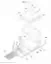
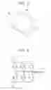
As illustrated in FIG. 1, a semiconductor module 10 includes a back-surface electrode plate 18, a semiconductor element 16, a spacer 14, a front-surface electrode plate 12, and so on. The semiconductor element 16 is an IGBT in which a diode is incorporated, and includes a back-surface electrode (in practice, a collector electrode) 16D, and a front-surface electrode (in practice, an emitter electrode) 16A. The back-surface electrode 16D expands over a whole area on a back surface of the semiconductor element 16, whereas the front-surface electrode 16A expands in a partial range on a front surface of the semiconductor element 16, and wire bond pads 16C are provided in a range 16B where the front-surface electrode 16A is not formed. In the figure, a reference numeral is assigned only to one wire bond pad, but a plurality of wire bond pads is provided in practice. The wire bonding pads include a pad connected to a gate electrode of the IGBT, a pad connected to a sensor for outputting a voltage indicative of a temperature of the IGBT, a pad connected to a sensor for outputting a voltage indicative of a conducting current of the IGBT, and the like.
The spacer 14 is constituted by a conductor, and a back surface of the spacer 14 is fixed to the front-surface electrode 16A with solder. A reference numeral 16B indicates a region that is not coated with the spacer 14, and the wire bond pads 16C are formed in a non-coating region 16B.
The front-surface electrode plate 12 is constituted by a conductor, and a back surface of the front-surface electrode plate 12 is fixed to a front surface of the spacer 14. The front-surface electrode plate 12 includes a flat portion 12A fixed to the front surface of the spacer 14, and a terminal portion 12B extending outside the after-mentioned molding resin. In the flat portion 12A, a stepped portion 12C that receives a flat portion 36 of the after-mentioned connection component 30 or a flat portion 46 of the after-mentioned connection component 40, and a stepped portion 12D that receives a flat portion 44 of the after-mentioned connection component 40 are formed.
The back-surface electrode plate 18 is constituted by a conductor, and includes a flat portion 18A fixed to the back-surface electrode 16D of the semiconductor element 16, a terminal portion 18B extending outside the after-mentioned molding resin, a group of bond portions 18E, and a group of pins 18F. The back-surface electrode 16D is fixed, with solder, to a front surface of the flat portion 18A of the back-surface electrode plate 18. In the flat portion 18A, a stepped portion 18D that receives a flat portion 32 of the after-mentioned connection component 30 or a flat portion 50 of the after-mentioned connection component 40, and a stepped portion 18C (not illustrated in FIG. 1) that receives a flat portion 52 of the after-mentioned connection component 40 are formed. In the figure, a reference numeral 18E is assigned only to one of the bond portions, and a reference numeral 18F is assigned only to one of the pins, but a plurality of bond portions and a plurality of pins are provided in practice. The pins 18F are formed into a linear shape so as to pass through respective bond portions 18E. Note that the pins 18F and the bond portions 18E may be in a positional relationship in which they are moved in parallel to each other only by a predetermined distance. In FIG. 1, only one bonding wire 20 is illustrated, but in practice, the pin and the bond portion in each set are connected to each other with the bonding wire 20.
A virtual line 22 of FIG. 1 indicates a filling range of the after-mentioned molding resin, a part on a right side relative to the virtual line 22 is sealed in the molding resin, and a part on a left side relative to the virtual line 22 extends outside the molding resin. The bonding wires 20 and the bond portions 18E are sealed in the molding resin. Virtual lines 24 indicate lines to be cut after the molding resin is formed, and when cutting is performed, the pins adjacent to each other are insulated from each other. The pin 18F extends to the bond portion 18E in the molding resin, and is connected to a gate electrode, a sensor, or the like in the semiconductor element 16 via the bonding wire 20.
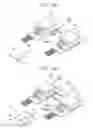
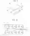
A reference numeral 30 illustrated in FIGS. 2A, 2B and the like indicates a first connection component, which is made of a conductive member (metal in the embodiment) and is configured such that the flat portion 32 and the flat portion 36 are connected via a connecting portion 34. The flat portion 32 has a shape to be received by the stepped portion 18D of the back-surface electrode plate 18. When the flat portion 32 is fitted to the stepped portion 18D, a back surface of the flat portion 18A is flush with a back surface of the flat portion 32. The flat portion 36 has a shape to be received by the stepped portion 12C of the front-surface electrode plate 12. When the flat portion 36 is fitted to the stepped portion 12C, a front surface of the flat portion 12A is flush with a front surface of the flat portion 36.
A reference numeral 40 indicates a second connection component, and is constituted by a front-side second connection component 42 and a back-side second connection component 48. The front-side second connection component 42 is constituted by a pair of flat portions 44, 46 and a connecting portion that connects them. The flat portion 44 has a shape to be received by the stepped portion 12D of the front-surface electrode plate 12. When the flat portion 44 is fitted to the stepped portion 12D, the front surface of the flat portion 12A is flush with a front surface of the flat portion 44. The flat portion 46 has a shape to be received by the stepped portion 12C of the front-surface electrode plate 12. When the flat portion 46 is fitted to the stepped portion 12C, the front surface of the flat portion 12A is flush with a front surface of the flat portion 46. The back-side second connection component 48 is constituted by a pair of flat portions 50, 52 and a connecting portion that connects them. The flat portion 50 has a shape to be received by the stepped portion 18D of the back-surface electrode plate 18. When the flat portion 50 is fitted to the stepped portion 18D, the back surface of the flat portion 18A is flush with a back surface of the flat portion 50. The flat portion 52 has a shape to be received by the c stepped portion 18C of the back-surface electrode plate 18. When the flat portion 52 is fitted to the stepped portion 18C, the back surface of the flat portion 18A is flush with a back surface of the flat portion 52. The front-side second connection component 42 and the back-side second connection component 48 may be integrated with each other by an insulating material.
FIG. 2A illustrates a case where two semiconductor modules 10, 110 are connected in series by the first connection component 30. The flat portion 32 is fitted to the stepped portion 18D of the module 10 on the left side out of the two semiconductor modules 10, 110 placed adjacent to each other, and then connected thereto with solder, and further, the flat portion 36 is fitted to a stepped portion 112C of the module 110 on the right side, and then connected thereto with solder. Hereby, the semiconductor modules 10, 110 are connected in series to each other. Note that, in order to distinguish the modules on the left side and the right side from each other, a reference numeral of the left semiconductor module is assumed 10, and a reference numeral of the right semiconductor module is assumed 110. However, the semiconductor modules are the same and compatible with each other. Further, in the following description, in terms of a member in the semiconductor module 110, a number obtained by adding 100 to its corresponding member number in the semiconductor module 10 is used, so that a redundant description thereof is omitted.
FIG. 2B illustrates a case where two semiconductor modules 10, 210 are connected in parallel by the second connection component 40. The flat portion 44 is fitted to the stepped portion 12D of the module 10 on the left side out of the two semiconductor modules 10, 210 placed adjacent to each other, and then connected thereto with solder, and the flat portion 46 is fitted to a stepped portion 212C of the module 210 on the right side and then connected thereto with solder. Further, the flat portion 50 is fitted to the stepped portion 18D of the module 10 on the left side and connected thereto with solder, and the flat portion 52 is fitted to a stepped portion 218C of the module 210 on the right side and connected thereto with solder. Hereby, the semiconductor modules 10, 210 are connected in parallel to each other. Here, in order to distinguish the modules on the left side and the right side, a reference numeral of the left semiconductor module is assumed 10, and a reference numeral of the right semiconductor module is assumed 210. However, the semiconductor modules are the same and compatible with each other. Further, in terms of a member in the semiconductor module 210, a number obtained by adding 200 to its corresponding member number in the semiconductor module 10 is used, so that a redundant description thereof is omitted.
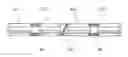
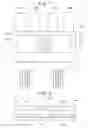
FIG. 3 is a plan view of the semiconductor device in a state where the assembly illustrated in FIG. 2A is set in an injection molding die and molding is performed. A reference numeral 60 indicates a molding resin. The terminal portions 12B, 18B of the semiconductor module 10 on the left side and terminal portions 112B, 118B of the semiconductor module 110 on the right side extend outside the molding resin 60. The pins 18F, 118F also extend outside the molding resin 60. When cutting is performed along the cutting lines 24 in FIG. 1 in this state, the pins are insulated from each other. Reference numerals 62, 64 indicate openings formed in the molding resin 60, and front surfaces of the flat portions 12A, 112A and the connection component 30 are exposed in the openings. Although not illustrated in the figure, back surfaces of the flat portions 18A, 118A and the connection component 30 are also exposed on a back surface of the molding resin 60.
FIG. 4 is a sectional view of the semiconductor device in FIG. 3, and FIG. 5 is a perspective view of the first connection component 30. A part inside a broken line in FIG. 6 indicates a circuit provided in the semiconductor device in FIG. 3. When three semiconductor devices in FIG. 3 are connected in parallel, a three-phase inverter circuit is obtained. The semiconductor device in FIG. 3 is used such that the terminal portion 12B (connected to an emitter) of the semiconductor module 10 is connected to a negative electrode of a direct-current power source, the terminal portion 118B (connected to a collector) of the semiconductor module 110 is connected to a positive electrode of the direct-current power source, and the terminal portion 18B of the semiconductor module 10 and the terminal portion 112B of the semiconductor module 110 (both have the same potential and are connected by the first connection component 30) are connected to a motor. Note that the sectional view of FIG. 4 is schematic, and the members 12, 14, 16, 18, 20, 30 are sealed with the molding resin.
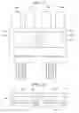
FIG. 7 is a plan view of the semiconductor device in a state where the assembly illustrated in FIG. 2B is set in an injection molding die and molding is performed. A reference numeral 60 indicates a molding resin. The terminal portions 12B, 18B of the semiconductor module 10 on the left side and terminal portions 212B, 218B of the semiconductor module 210 on the right side extend outside the molding resin 60. The pins 18F, 218F also extend outside the molding resin 60. When cutting is performed along the cutting lines 24 in FIG. 1 in this state, the pins are insulated from each other. Reference numerals 62, 64 indicate openings formed in the molding resin 60, and front surfaces of the flat portions 12A, 212A and the connection component 40 are exposed in the openings. Although not illustrated in the figure, back surfaces of the flat portions 18A, 218A and the connection component 40 are also exposed on a back surface of the molding resin 60.
FIG. 8 is a sectional view of the semiconductor device in FIG. 7, and FIG. 9 is a perspective view of the second connection component 40. A part inside a broken line in FIG. 10 indicates a circuit provided in the semiconductor device in FIG. 7. For example, an inverter circuit for an electric vehicle deals with a heavy current, so it might be difficult to constitute one phase by one semiconductor element. It might be necessary to connect two semiconductor elements in parallel, so as to constitute one phase. The semiconductor device of FIG. 7 can deal with such a necessity. When two semiconductor devices in FIG. 7 are connected in series, one phase in the inverter circuit is obtained. For that purpose, two semiconductor devices in FIG. 7 are used such that they are connected in series. In a semiconductor device on an upper side (an upper arm), one or both of terminal portions 18B and 218B (both at the same potential) are connected to a positive electrode of a direct-current power source. In a semiconductor device on a lower side (a lower arm), one or both of terminal portions 12B and 212B (both at the same potential) are connected to a negative electrode of the direct-current power source. The terminal portions 12B and 212B (both at the same potential) of the semiconductor device on the upper side and the terminal portions 18B and 218B (both at the same potential) of the semiconductor device on the lower side are used by being connected to a motor. Note that the sectional view of FIG. 8 is schematic, and the members 12, 14, 16, 18, 20, 40 are sealed with the molding resin. The molding resin is also filled into a space between the front-side second connection component 42 and the back-side second connection component 48.
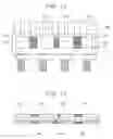
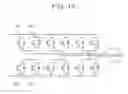
FIG. 11 illustrates a semiconductor device configured such that an assembly in which a first semiconductor module 10 and a second semiconductor module 310 are connected to each other by the second connection component 40 (corresponding to the assembly in FIG. 2B), the second semiconductor module 310 and a third semiconductor module 410 are connected to each other by the first connection component 30 (corresponding to the assembly of FIG. 2A), and the third semiconductor module 410 and a fourth semiconductor module 510 are connected to each other by the second connection component 40 (corresponding to the assembly of FIG. 2B) is integrated by a molding resin. A part inside a broken line in FIG. 13 indicates a circuit provided in the semiconductor device in FIG. 11. When three semiconductor devices in FIG. 11 are connected in parallel, a three-phase inverter circuit is obtained.
The above descriptions show merely a part of the embodiment, and various modifications can be made. For example, with the use of three semiconductor modules and two first connection components, it is possible to obtain a semiconductor device in which the three semiconductor devices are connected in series. With the use of three semiconductor modules and two second connection components, it is possible to obtain a semiconductor device in which the three semiconductor devices are connected in parallel.
The concrete examples of the disclosure have been described in detail, but these are merely examples and do not limit the disclosure according to Claims. A technique according to Claims includes embodiments obtained by variously modifying or altering the concrete examples exemplified as above. Technical elements described in the present specification or the drawings exhibit a technical usability solely or in various combinations, and are not limited to combinations as described in Claims as of filing the present application. Further, the technique exemplified in the present specification or the drawings can achieve a plurality of objects at the same time, and has a technical usability by achieving one of those objects.
Claims
What is claimed is:1. A semiconductor device comprising:
an assembly configured such that a plurality of semiconductor modules is connected by a connection component, the assembly being sealed with a molding resin, wherein:
each of the plurality of semiconductor modules includes
a semiconductor element including a front-surface electrode and a back-surface electrode,
a front-surface electrode plate fixed to the front-surface electrode, and
a back-surface electrode plate fixed to the back-surface electrode;
the connection component is either of a first connection component and a second connection component, the first connection component being configured to connect adjacent semiconductor modules to each other such that a front-surface electrode plate of one of the adjacent semiconductor modules is connected to a back-surface electrode plate of the other one of the adjacent semiconductor modules, the second connection component being configured to connect adjacent semiconductor modules to each other such that respective front-surface electrode plates are connected to each other and respective back-surface electrode plates are connected to each other; and
the adjacent semiconductor modules are configured to be connected to each other by the first connection component or the second connection component.
2. A semiconductor device comprising:
a first semiconductor module including a first semiconductor element including a first front-surface electrode and a first back-surface electrode, a first front-surface electrode plate fixed to the first front-surface electrode, and a first back-surface electrode plate fixed to the first back-surface electrode;
a second semiconductor module including a second semiconductor element including a second front-surface electrode and a second back-surface electrode, a second front-surface electrode plate fixed to the second front-surface electrode, and a second back-surface electrode plate fixed to the second back-surface electrode;
a connection component configured to connect the first front-surface electrode plate to the second back-surface electrode plate; and
a molding resin configured to seal the first semiconductor module, the second semiconductor module, and the connection component.
3. The semiconductor device according to claim 2, wherein
the first front-surface electrode, the second back-surface electrode, and the connection component are partially exposed from the molding resin.
4. A semiconductor device comprising:
a first semiconductor module including a first semiconductor element including a first front-surface electrode and a first back-surface electrode, a first front-surface electrode plate fixed to the first front-surface electrode, and a first back-surface electrode plate fixed to the first back-surface electrode;
a second semiconductor module including a second semiconductor element including a second front-surface electrode and a second back-surface electrode, a second front-surface electrode plate fixed to the second front-surface electrode, and a second back-surface electrode plate fixed to the second back-surface electrode;
a first connection component configured to connect the first front-surface electrode plate to the second front-surface electrode plate;
a second connection component configured to connect the first back-surface electrode plate to the second back-surface electrode plate; and
a molding resin configured to seal the first semiconductor module, the second semiconductor module, the first connection component, and the second connection component.
5. The semiconductor device according to claim 4, wherein
the first front-surface electrode, the second front-surface electrode, and the first connection component are partially exposed from the molding resin.
6. The semiconductor device according to claim 4, wherein
the first back-surface electrode, the second back-surface electrode, and the second connection component are partially exposed from the molding resin.
7. The semiconductor device according to claim 4, wherein
the first connection component and the second connection component are integrated with each other by an insulating material.
Images & Drawings included:
Sources:
- United States Patent and Trademark Office - verify current appl. status at the USPTO↗
Recent applications in this class:
- » 20250293171 2025-09-18
SEMICONDUCTOR PACKAGE DEVICE AND METHOD OF MANUFACTURING THE SAME - » 20250285985 2025-09-11
SELECTIVE USE OF DIFFERENT ADVANCED INTERFACE BUS WITH ELECTRONIC CHIPS - » 20250279369 2025-09-04
CIRCUIT BOARD - » 20250273584 2025-08-28
CONNECTING MULTIPLE CHIPS USING AN INTERCONNECT DEVICE - » 20250273583 2025-08-28
INTERPOSER DEVICE AND SEMICONDUCTOR PACKAGE DEVICE - » 20250273582 2025-08-28
INTERCONNECTIONS TO PACKAGE SUBSTRATES FOR INTERCONNECT BRIDGES - » 20250259939 2025-08-14
PHOTONICS INTEGRATED CIRCUIT PACKAGE - » 20250259938 2025-08-14
SEMICONDUCTOR PACKAGE - » 20250259937 2025-08-14
SQUARE THERMAL VIA - » 20250253259 2025-08-07
METHODS AND APPARATUS TO COMPENSATE FOR IMPEDANCE AND REDUCE CROSSTALK IN INTEGRATED CIRCUIT PACKAGES
Recent applications for this Assignee:
- » 20250294012 2025-09-18
GATEWAY DEVICE - » 20250293858 2025-09-18
SYSTEMS AND METHODS FOR SECURELY MANAGING ACCESS TO VEHICLE DATA - » 20250293569 2025-09-18
COOLING STRUCTURE - » 20250293539 2025-09-18
REDUNDANT POWER SUPPLY SYSTEM - » 20250293469 2025-09-18
CONNECTOR MOUNTING STRUCTURE - » 20250293409 2025-09-18
ELECTRICITY STORAGE CELL - » 20250293401 2025-09-18
CELL STACK - » 20250293400 2025-09-18
STORAGE CELL - » 20250293399 2025-09-18
POWER STORAGE CELL AND METHOD FOR MANUFACTURING THE SAME - » 20250293381 2025-09-18
POWER STORAGE DEVICE AND VEHICLE