UNITY SEMICONDUCTOR CORPORATION
Sunnyvale, California
United States
258
2020-08-06
214
2021-08-10
Top Inventors for applications by UNITY SEMICONDUCTOR CORPORATION
These are the the leading inventors for applications assigned to UNITY SEMICONDUCTOR CORPORATION:
- Robert Norman 97 Pendleton, OR United States
- Darrell Rinerson 57 Cupertino, CA United States
- Christophe Chevallier 54 Palo Alto, CA United States
- Chang Hua Siau 47 Saratoga, CA United States
- Christophe J. Chevallier 44 Palo Alto, CA United States
- Wayne Kinney 29 Emmett, ID United States
- Lawrence Schloss 28 Palo Alto, CA United States
- STEVEN W. LONGCOR 21 MOUNTAIN VIEW, CA United States
- Roy Lambertson 16 Los Altos, CA United States
- Edmond Ward 16 Monte Sereno, CA United States
- Steve Kuo-Ren Hsia 15 San Jose, CA United States
- Robin Cheung 14 Cupertino, CA United States
- Rene Meyer 13 Atherton, CA United States
- Edmond R. Ward 13 Monte Sereno, CA United States
- Bruce Lynn Bateman 13 Fremont, CA United States
- Seow Fong Lim 13 Fremont, CA United States
- Chang Hua Siau 12 San Jose, CA United States
- Jonathan Bornstein 11 Cupertino, CA United States
- Philip Swab 10 Santa Rosa, CA United States
- David Hansen 10 Palo Alto, CA United States
- John Sanchez 10 Palo Alto, CA United States
- Julie Casperson Brewer 9 Santa Clara, CA United States
- John E. Sanchez, JR. 9 Palo Alto, CA United States
- Steven Longcor 9 Mountain View, CA United States
- Wayne Kinney 9 Emmett, CA United States
- Philip F.S. Swab 8 Santa Rosa, CA United States
- Robert Norman 7 Blaine, WA United States
- PHILIP F. S. SWAB 7 SANTA ROSA, CA United States
- DAVID EGGLESTON 7 SAN JOSE, CA United States
- Travis Byonghyop Oh 7 San Jose, CA United States
- Jon Bornstein 6 Cupertino, CA United States
- Rene Meyer 6 Mountain View, CA United States
- LIDIA VEREEN 6 SAN RAMON, CA United States
- Julie Casperson Brewer 5 New York, NY United States
- BRUCE BATEMAN 5 FREMONT, CA United States
- Jian Wu 5 San Jose, CA United States
- LOUIS PARRILLO 4 AUSTIN, TX United States
- Julie Casperson Brewer 4 Hoboken, NJ United States
- Sri Rama Namala 4 San Jose, CA United States
- Wen Zhong Kong 3 Newark, CA United States
- Chang Hua Siau 3 Sunnyvale, CA United States
- Sri Namala 3 San Jose, CA United States
- Christophe Chevallier 3 Sunnyvale, CA United States
- Rene Meyer 3 Fremont, CA United States
- Elizabeth Friend 2 Sunnyvale, CA United States
- John Sanchez, Jr. 2 Palo Alto, CA United States
- John E. Sanchez 2 Palo Alto, CA United States
- LOUIS C. PARRILLO 2 AUSTIN, TX United States
- David A. Eggleston 2 San Jose, CA United States
- Bruce L. Bateman 2 Fremont, CA United States
- Travis Byonghyop 1 San Jose, CA United States
- Edmond B. Ward 1 Monte Sereno, CA United States
- Chang Hua Siau 1 Sararoga, CA United States
- Philip F.S. Swab 1 Santa Rose, CA United States
- Robert Norman 1 Pendelton, OR United States
- Darrell Rinerson 1 , United States
- Edmond R. Ward 1 Mount Sereno, CA United States
- Unity Semiconductor Corporation 1 Sunnyvale, CA United States
- Darrel Rinerson 1 Cupertino, CA United States
- Christophe Chavellier 1 Palo Alto, CA United States
- Steve Hsia 1 San Jose, CA United States
- Roy Lamberston 1 Los Altos, CA United States
- Christrophe J. Chevallier 1 Palo Alto, CA United States
- Robert Norman 1 Sunnyvale, CA United States
- Paul Besser 1 Sunnyvale, CA United States
- Mary Calarrudo 1 Santa Clara, CA United States
- Julie Casperson Brewer 1 Noboken, NJ United States
- David Hasen 1 Palo Alto, CA United States
- Christoophe J. Chevallier 1 Palo alto, CA United States
- Louis Parillo 1 Austin, TX United States
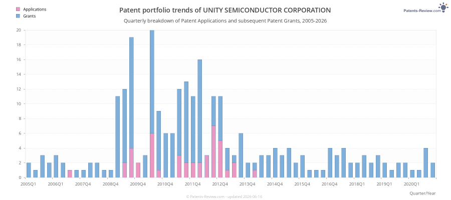
Recent patent applications by UNITY SEMICONDUCTOR CORPORATION
UNITY SEMICONDUCTOR CORPORATION based in Sunnyvale, US has been assigned the rights to these inventions. The list includes both Pending Applications and Patent Grants:
US20200251167A1
PhysicsGlobal bit line pre-charge circuit that compensates for process, operating voltage, and temperature variations
#2 | 2020-01-09 ✅ Patent 10,614,882 granted on 2020-04-07US20200013460A1
PhysicsAccess signal adjustment circuits and methods for memory cells in a cross-point array
#3 | 2019-12-26 ✅ Patent 10,672,467 granted on 2020-06-02US20190392895A1
PhysicsHigh voltage switching circuitry for a cross-point array
#4 | 2019-09-12 ✅ Patent 10,566,056 granted on 2020-02-18US20190279712A1
PhysicsGlobal bit line pre-charge circuit that compensates for process, operating voltage, and temperature variations
#5 | 2019-08-15 ✅ Patent 10,650,870 granted on 2020-05-12US20190252011A1
PhysicsCircuits and techniques to compensate memory access signals for variations of parameters in multiple layers of memory
#6 | 2019-04-04 ✅ Patent 10,354,726 granted on 2019-07-16US20190103161A1
PhysicsAccess signal adjustment circuits and methods for memory cells in a cross-point array
#7 | 2019-02-14 ✅ Patent 10,529,778 granted on 2020-01-07US20190051701A1
ElectricityVertical cross-point memory arrays
#8 | 2019-01-10 ✅ Patent 10,347,332 granted on 2019-07-09US20190013070A1
PhysicsHigh voltage switching circuitry for a cross-point array
#9 | 2018-12-20 ✅ Patent 10,229,739 granted on 2019-03-12US20180366194A9
PhysicsGLOBAL BIT LINE PRE-CHARGE CIRCUIT THAT COMPENSATES FOR PROCESS, OPERATING VOLTAGE, AND TEMPERATURE VARIATIONS
#10 | 2018-12-20 ✅ Patent 10,585,603 granted on 2020-03-10US20180364931A1
PhysicsArray voltage regulating technique to enable data operations on large memory arrays with resistive memory elements
#11 | 2018-11-29 ✅ Patent 10,622,028 granted on 2020-04-14US20180342268A1
PhysicsLocal bit lines and methods of selecting the same to access memory elements in cross-point arrays
#12 | 2018-08-09 ✅ Patent 10,210,917 granted on 2019-02-19US20180226110A1
PhysicsCircuits and techniques to compensate memory access signals for variations of parameters in multiple layers of memory
#13 | 2018-07-12 ✅ Patent 10,229,739 granted on 2019-03-12US20180197604A1
PhysicsGlobal bit line pre-charge circuit that compensates for process, operating voltage, and temperature variations
#14 | 2018-06-28 ✅ Patent 10,453,525 granted on 2019-10-22US20180182454A1
PhysicsPreservation circuit and methods to maintain values representing data in one or more layers of memory
#15 | 2018-04-26 ✅ Patent 10,311,950 granted on 2019-06-04US20180114573A1
PhysicsConductive metal oxide structures in non-volatile re-writable memory devices
#16 | 2018-04-05 ✅ Patent 10,074,420 granted on 2018-09-11US20180096726A1
PhysicsAccess signal adjustment circuits and methods for memory cells in a cross-point array
#17 | 2018-01-04 ✅ Patent 9,997,241 granted on 2018-06-12US20180005694A1
PhysicsHigh voltage switching circuitry for a cross-point array
#18 | 2017-12-21 ✅ Patent 10,031,686 granted on 2018-07-24US20170364296A1
PhysicsArray voltage regulating technique to enable data operations on large memory arrays with resistive memory elements
#19 | 2017-11-09 ✅ Patent 9,870,823 granted on 2018-01-16US20170323681A1
PhysicsGlobal bit line pre-charge circuit that compensates for process, operating voltage, and temperature variations
#20 | 2017-06-22 ✅ Patent 9,806,130 granted on 2017-10-31US20170179197A1
ElectricityMemory element with a reactive metal layer
#21 | 2017-06-08 ✅ Patent 9,830,985 granted on 2017-11-28US20170162261A1
PhysicsPreservation circuit and methods to maintain values representing data in one or more layers of memory
#22 | 2017-05-18 ✅ Patent 9,767,899 granted on 2017-09-19US20170140816A1
PhysicsAccess signal conditioning for memory cells in an array
#23 | 2017-04-20 ✅ Patent 9,818,799 granted on 2017-11-14US20170110514A1
ElectricityMulti-layered conductive metal oxide structures and methods for facilitating enhanced performance characteristics of two-terminal memory cells
#24 | 2017-02-02 ✅ Patent 10,050,086 granted on 2018-08-14US20170033158A1
ElectricityVertical cross-point memory arrays
#25 | 2017-01-26 ✅ Patent 9,711,212 granted on 2017-07-18US20170025173A1
PhysicsHigh voltage switching circuitry for a cross-point array
#26 | 2017-01-12 ✅ Patent 9,720,611 granted on 2017-08-01US20170010831A1
PhysicsArray voltage regulating technique to enable data operations on large memory arrays with resistive memory elements
#27 | 2016-12-29 ✅ Patent 9,870,809 granted on 2018-01-16US20160379692A1
PhysicsCircuits and techniques to compensate memory access signals for variations of parameters in multiple layers of memory
#28 | 2016-11-03 ✅ Patent 9,691,480 granted on 2017-06-27US20160322104A1
PhysicsGlobal bit line pre-charge circuit that compensates for process, operating voltage, and temperature variations
#29 | 2016-10-13 ✅ Patent 9,691,821 granted on 2017-06-27US20160300883A1
ElectricityVertical cross-point arrays for ultra-high-density memory applications
#30 | 2016-09-15 ✅ Patent 9,767,897 granted on 2017-09-19US20160267973A1
PhysicsConductive metal oxide structures in non-volatile re-writable memory devices
#31 | 2016-06-16 ✅ Patent 9,514,811 granted on 2016-12-06US20160172025A1
PhysicsAccess signal adjustment circuits and methods for memory cells in a cross-point array
#32 | 2016-01-07 ✅ Patent 9,570,515 granted on 2017-02-14US20160005793A1
ElectricityMemory element with a reactive metal layer
#33 | 2015-12-31 ✅ Patent 9,831,425 granted on 2017-11-28US20150380642A1
ElectricityTwo-terminal reversibly switchable memory device
#34 | 2015-12-17 ✅ Patent 9,384,806 granted on 2016-07-05US20150364169A1
PhysicsCircuits and techniques to compensate memory access signals for variations of parameters in multiple layers of memory
#35 | 2015-10-22 ✅ Patent 9,390,796 granted on 2016-07-12US20150302923A1
PhysicsGlobal bit line pre-charge circuit that compensates for process, operating voltage, and temperature variations
#36 | 2015-09-17 ✅ Patent 9,536,607 granted on 2017-01-03US20150262664A1
PhysicsPreservation circuit and methods to maintain values representing data in one or more layers of memory
#37 | 2015-08-06 ✅ Patent 9,306,549 granted on 2016-04-05US20150222251A1
ElectricityHigh voltage switching circuitry for a cross-point array
#38 | 2015-06-25 ✅ Patent 9,299,427 granted on 2016-03-29US20150179250A1
PhysicsAccess signal adjustment circuits and methods for memory cells in a cross-point array
#39 | 2015-05-21 ✅ Patent 9,401,202 granted on 2016-07-26US20150138874A1
PhysicsArray voltage regulating technique to enable data operations on large memory arrays with resistive memory elements
#40 | 2015-05-14 ✅ Patent 10,002,646 granted on 2018-06-19US20150132917A1
ElectricityLocal bit lines and methods of selecting the same to access memory elements in cross-point arrays
#41 | 2015-04-09 ✅ Patent 9,312,307 granted on 2016-04-12US20150097155A1
ElectricityVertical cross point arrays for ultra high density memory applications
#42 | 2015-02-26 ✅ Patent 9,129,668 granted on 2015-09-08US20150055425A1
PhysicsCircuits and techniques to compensate memory access signals for variations of parameters in multiple layers of memory
#43 | 2015-01-29 ✅ Patent 9,159,913 granted on 2015-10-13US20150029780A1
ElectricityTwo-terminal reversibly switchable memory device
#44 | 2015-01-15 ✅ Patent 9,570,459 granted on 2017-02-14US20150014760A1
ElectricityVertical gate NAND memory devices
#45 | 2014-12-18 ✅ Patent 9,047,928 granted on 2015-06-02US20140369151A1
PhysicsHigh voltage switching circuitry for a cross-point array
#46 | 2014-12-18 ✅ Patent 9,293,702 granted on 2016-03-22US20140367629A1
ElectricityConductive metal oxide structures in non-volatile re-writable memory devices
#47 | 2014-11-27 ✅ Patent 9,484,533 granted on 2016-11-01US20140346435A1
ElectricityMulti-layered conductive metal oxide structures and methods for facilitating enhanced performance characteristics of two-terminal memory cells
#48 | 2014-11-13 ✅ Patent 9,368,200 granted on 2016-06-14US20140334222A1
PhysicsLow read current architecture for memory
#49 | 2014-08-21 ✅ Patent 9,029,827 granted on 2015-05-12US20140231741A1
ElectricityPlanar resistive memory integration
#50 | 2014-08-07 ✅ Patent 8,988,930 granted on 2015-03-24US20140219006A1
PhysicsAccess signal adjustment circuits and methods for memory cells in a cross-point array
#51 | 2014-07-31 ✅ Patent 9,159,408 granted on 2015-10-13US20140211542A1
PhysicsMemory element with a reactive metal layer
#52 | 2014-05-22 ✅ Patent 9,053,756 granted on 2015-06-09US20140140123A1
PhysicsPreservation circuit and methods to maintain values representing data in one or more layers of memory
#53 | 2014-05-22 ✅ Patent 8,929,126 granted on 2015-01-06US20140140122A1
PhysicsArray voltage regulating technique to enable data operations on large cross-point memory arrays with resistive memory elements
#54 | 2014-05-22 ✅ Patent 8,901,962 granted on 2014-12-02US20140139264A1
ElectricityProgrammable logic device structure using third dimensional memory
#55 | 2014-01-16US20140014893A1
ElectricityARRAY OPERATION USING A SCHOTTKY DIODE AS A NON-OHMIC SELECTION DEVICE
#56 | 2014-01-09 ✅ Patent 8,848,425 granted on 2014-09-30US20140009998A1
PhysicsConductive metal oxide structures in non volatile re-writable memory devices
#57 | 2013-11-21 ✅ Patent 8,854,888 granted on 2014-10-07US20130308410A1
PhysicsHigh voltage switching circuitry for a cross-point array
#58 | 2013-11-07 ✅ Patent 9,117,495 granted on 2015-08-25US20130294136A1
PhysicsGlobal bit line pre-charge circuit that compensates for process, operating voltage, and temperature variations
#59 | 2013-09-05 ✅ Patent 8,854,881 granted on 2014-10-07US20130229856A1
PhysicsCircuits and techniques to compensate memory access signals for variations of parameters in multiple layers of memory
#60 | 2013-08-29 ✅ Patent 9,112,499 granted on 2015-08-18US20130222010A1
ElectricityField programmable gate arrays using resistivity-sensitive memories
#61 | 2013-08-22 ✅ Patent 8,705,260 granted on 2014-04-22US20130215667A1
PhysicsCircuits and techniques to compensate data signals for variations of parameters affecting memory cells in cross point arrays
#62 | 2013-08-22 ✅ Patent 8,565,006 granted on 2013-10-22US20130214233A1
ElectricityConductive metal oxide structures in non volatile re writable memory devices
#63 | 2013-08-15 ✅ Patent 9,419,217 granted on 2016-08-16US20130210211A1
ElectricityVertical cross-point memory arrays
#64 | 2013-08-15 ✅ Patent 8,610,099 granted on 2013-12-17US20130207066A1
ElectricityPlanar resistive memory integration
#65 | 2013-05-30 ✅ Patent 8,654,565 granted on 2014-02-18US20130135920A1
PhysicsAccess signal adjustment circuits and methods for memory cells in a cross-point array
#66 | 2013-04-04US20130082232A1
ElectricityMulti Layered Conductive Metal Oxide Structures And Methods For Facilitating Enhanced Performance Characteristics Of Two Terminal Memory Cells
#67 | 2013-04-04US20130082228A1
ElectricityMemory Device Using Multiple Tunnel Oxide Layers
#68 | 2013-03-07 ✅ Patent 8,569,160 granted on 2013-10-29US20130059436A1
PhysicsDevice fabrication
#69 | 2013-02-21 ✅ Patent 8,937,292 granted on 2015-01-20US20130043455A1
ElectricityVertical cross point arrays for ultra high density memory applications
#70 | 2013-02-21US20130043452A1
ElectricityStructures And Methods For Facilitating Enhanced Cycling Endurance Of Memory Accesses To Re-Writable Non Volatile Two Terminal Memory Elements
#71 | 2013-01-03 ✅ Patent 8,565,003 granted on 2013-10-22US20130003437A1
ElectricityMultilayer cross-point memory array having reduced disturb susceptibility
#72 | 2012-12-13 ✅ Patent 8,361,560 granted on 2013-01-29US20120315503A1
Chemistry; metallurgyImmersion platinum plating solution
#73 | 2012-12-13 ✅ Patent 8,559,209 granted on 2013-10-15US20120314477A1
PhysicsArray voltage regulating technique to enable data operations on large cross-point memory arrays with resistive memory elements
#74 | 2012-12-13 ✅ Patent 8,891,276 granted on 2014-11-18US20120314468A1
PhysicsMemory array with local bitlines and local-to-global bitline pass gates and gain stages
#75 | 2012-12-06 ✅ Patent 8,897,050 granted on 2014-11-25US20120307542A1
PhysicsLocal bit lines and methods of selecting the same to access memory elements in cross-point arrays
#76 | 2012-11-29 ✅ Patent 8,493,771 granted on 2013-07-23US20120300535A1
PhysicsNon-volatile memory device ion barrier
#77 | 2012-11-22US20120292585A1
ElectricityCONTINUOUS PLANE OF THIN-FILM MATERIALS FOR A TWO-TERMINAL CROSS-POINT MEMORY
#78 | 2012-11-15 ✅ Patent 8,565,039 granted on 2013-10-22US20120286232A1
ElectricityArray operation using a schottky diode as a non-ohmic selection device
#79 | 2012-10-18US20120265929A1
PhysicsINTEGRATED CIRCUITS TO CONTROL ACCESS TO MULTIPLE LAYERS OF MEMORY IN A SOLID STATE DRIVE
#80 | 2012-10-18US20120262981A1
PhysicsDATA RETENTION STRUCTURE FOR NON-VOLATILE MEMORY
#81 | 2012-10-11US20120257460A1
PhysicsMETHOD FOR INDICATING A NON-FLASH NONVOLATILE MULTIPLE-TYPE THREE-DIMENSIONAL MEMORY
#82 | 2012-10-11US20120257438A1
PhysicsCONTEMPORANEOUS MARGIN VERIFICATION AND MEMORY ACCESS FOR MEMORY CELLS IN CROSS POINT MEMORY ARRAYS
#83 | 2012-08-30US20120217466A1
ElectricityDigital Potentiometer Using Third Dimensional Memory
#84 | 2012-08-23US20120212646A1
ElectricityMemory Emulation In An Image Capture Device
#85 | 2012-08-23US20120211716A1
ElectricityOxygen ion implanted conductive metal oxide re-writeable non-volatile memory device
#86 | 2012-08-16US20120210053A1
PhysicsSecuring Non Volatile Data In RRAM
#87 | 2012-08-16US20120210052A1
ElectricityINTEGRATED CIRCUIT WITH COMPRESS ENGINE
#88 | 2012-08-16US20120208595A1
PhysicsMemory Emulation In A Cellular Telephone
#89 | 2012-08-16 ✅ Patent 8,588,005 granted on 2013-11-19US20120206980A1
PhysicsBuffering systems for accessing multiple layers of memory in integrated circuits
#90 | 2012-08-09 ✅ Patent 8,395,929 granted on 2013-03-12US20120201086A1
PhysicsSignal margin improvement for read operations in a cross-point memory array
#91 | 2012-07-12US20120179862A1
PhysicsSystem For Accessing Non-Volatile Memory
#92 | 2012-07-12 ✅ Patent 8,347,254 granted on 2013-01-01US20120176840A1
ElectricityCombined memories in integrated circuits
#93 | 2012-07-12 ✅ Patent 8,305,796 granted on 2012-11-06US20120176832A1
PhysicsAccess signal adjustment circuits and methods for memory cells in a cross-point array
#94 | 2012-06-14US20120147678A1
PhysicsBuffering Systems For Accessing Multiple Layers Of Memory In Integrated Circuits
#95 | 2012-06-14US20120147660A1
PhysicsPreservation Circuit And Methods To Maintain Values Representing Data In One Or More Layers Of Memory
#96 | 2012-04-12US20120087174A1
ElectricityTwo Terminal Re Writeable Non Volatile Ion Transport Memory Device
#97 | 2012-03-29 ✅ Patent 8,737,151 granted on 2014-05-27US20120075914A1
PhysicsLow read current architecture for memory
#98 | 2012-03-22 ✅ Patent 8,255,619 granted on 2012-08-28US20120069665A1
PhysicsMemory device with vertically embedded non flash non volatile memory for emulation of NAND flash memory
#99 | 2012-03-22 ✅ Patent 8,270,196 granted on 2012-09-18US20120069621A1
PhysicsIntegrated circuits using non volatile resistivity sensitive memory for emulation of embedded flash memory
#100 | 2012-03-22 ✅ Patent 8,289,803 granted on 2012-10-16US20120069620A1
PhysicsSystem including vertically stacked embedded non-flash re-writable non-volatile memory
Also check out Unity Semiconductor Corporation's (Sunnyvale, United States) applicant profile with 68 patent applications submitted.
1226 ⎘