MEMC Electronic Materials, Inc.
St. Peters, Missouri
United States
216
2014-09-18
151
2015-11-24
Top Inventors for applications by MEMC Electronic Materials, Inc.
These are the the leading inventors for applications assigned to MEMC Electronic Materials, Inc.:
- Robert J. Falster 29 London, United Kingdom
- Puneet Gupta 29 Houston, TX United States
- Jeffrey L. Libbert 20 O'Fallon, MO United States
- MEMC Electronic Materials, Inc. 19 St. Peters, MO United States
- Satish Bhusarapu 19 Houston, TX United States
- Steven L. Kimbel 15 St. Charles, MO United States
- Henry F. Erk 13 St. Louis, MO United States
- Roland R. Vandamme 12 Wentzville, MO United States
- Alexis Grabbe 10 St. Charles, MO United States
- John A. Pitney 10 St. Peters, MO United States
- Jameel Ibrahim 10 Humble, TX United States
- Vladimir V. Voronkov 10 Merano, Italy
- Lu Fei 9 St. Louis, MO United States
- Vithal Revankar 9 Seabrook, TX United States
- Joseph C. Holzer 9 St. Charles, MO United States
- Milind S. Kulkarni 9 St. Louis, MO United States
- Mohsen Banan 9 Grover, MO United States
- Guoqiang David Zhang 8 Ballwin, MO United States
- Yue Huang 8 Midlothian, VA United States
- Milind Kulkarni 7 St. Louis, MO United States
- Harold W. Korb 7 Chesterfield, MO United States
- Zhihui Gu 7 Houston, TX United States
- Larry W. Shive 7 St. Charles, MO United States
- Lance G. Hellwig 7 Florissant, MO United States
- Paolo Mutti 7 Milan, Italy
- Peter D. Albrecht 7 O'Fallon, MO United States
- Marco Ravani 6 Novara, Italy
- Robert W. Standley 6 Chesterfield, MO United States
- Daniela Gambaro 5 Galliate, Italy
- Larry Wayne Shive 5 St. Charles, MO United States
- Larry Flannery 5 Warrenton, MO United States
- Roland Vandamme 5 Wentzville, MO United States
- Richard J. Phillips 5 St. Peters, MO United States
- Manabu Hamano 5 Utsunomiya, Japan
- Manabu Hamano 5 Utsunomiya-City, Japan
- Luca Moiraghi 5 Milano, Italy
- Brian L. Gilmore 5 O'Fallon, MO United States
- Shailendra B. Rathod 4 St. Louis, MO United States
- Milind S. Bhagavat 4 Medford, MA United States
- John Allen Pitney 4 St. Peters, MO United States
- Puneet Gupta 4 Singapore, Singapore
- Judith A. Schmidt 4 Troy, MO United States
- Massimiliano Olmo 4 Novara, Italy
- Bayard K. Johnson 4 Jefferson Hills, PA United States
- Chanrae Cho 4 Austin, TX United States
- Thomas E. Doane 4 Troy, MO United States
- Hariprasad Sreedharamurthy 4 Ballwin, MO United States
- Tracy M. Ragan 4 Warrenton, MO United States
- Marco Cornara 4 Galliate, Italy
- Michael R. Seacrist 4 Lake Saint Louis, MO United States
- Zheng Lu 4 St. Charles, MO United States
- Seamus A. McQuaid 4 Vitoria, Spain
- Michael J. Ries 3 St. Charles, MO United States
- Guoqiang Zhang 3 Ballwin, MO United States
- Dale A. Witte 3 Wentzville, MO United States
- Gregory M. Wilson 3 Chesterfield, MO United States
- Timothy Dinh Truong 3 Pearland, TX United States
- Steve A. Markgraf 3 Maple Grove, MN United States
- Brian Lawrence Gilmore 3 Allen, TX United States
- Thomas A. Torack 3 Oakland, MO United States
- Balaji Devulapalli 3 Chesterfield, MO United States
- Harold Korb 3 Chesterfield, MO United States
- John Davis Holder 3 Knoxville, TN United States
- Mark G. Stinson 3 Wood River, IL United States
- Brian Lawrence Gilmore 3 Foristell, MO United States
- Vandan Tanna 3 Dardenne Prairie, MO United States
- Hiroyo Haga 3 Utsunomiya, Japan
- Kwasi Foli 3 Columbia, MD United States
- Francesco Bonoli 3 Novara, Italy
- Lu Fei 3 St. Peters, MO United States
- Eugene R. Hollander 3 Foristell, MO United States
- Tomomi Komura 3 Utsunomiya, Japan
- Massoud Javidi 3 St. Peters, MO United States
- Mark G. Stinson 3 East Alton, IL United States
- Harold W. Korb 2 Town & Country, MO United States
- Richard G. Schrenker 2 Chesterfield, MO United States
- Yue Huang 2 Modlothian, VA United States
- Vladimir Voronkov 2 Merano, Italy
- John F. Valley 2 Lake Oswego, OR United States
- Takaaki Aoshima 2 Utsunomiya, Japan
- Mick Bjelopavlic 2 O'Fallon, MO United States
- Ichiro Yoshimura 2 Utsunomiya City, Japan
- Ichiro Yoshimura 2 Utsunomiya, Japan
- Baisheng Zou 2 Pearland, TX United States
- Srikanth Kommu 2 St. Charles, MO United States
- Madhavan S. Esayanur 2 St. Peters, MO United States
- Tomomi Komura 2 Tochigi, Japan
- Chang Bum Kim 2 St. Louis, MO United States
- Puneet Gupta 2 St. Louis, MO United States
- Sumeet S. Bhagavat 2 St. Charles, MO United States
- Antonio Maria Rinaldi 2 Novara, Italy
- Michael R. SEACRIST 2 St. Peters, MO United States
- Emanuele Corsi 2 Novara, Italy
- Milind S. Bhagavat 2 St. Peters, MO United States
- Anca Stefanescu 2 St. Charles, MO United States
- Richard J. Phillips 2 St. Charles, MO United States
- Sumeet S. Bhagavat 2 St. Peters, MO United States
- Takuto Kazama 2 Tochigi Prefecture, Japan
- Brian Lawrence Gilmore 2 O'Fallon, MO United States
- John Michael Pogany 2 St. Peters, MO United States
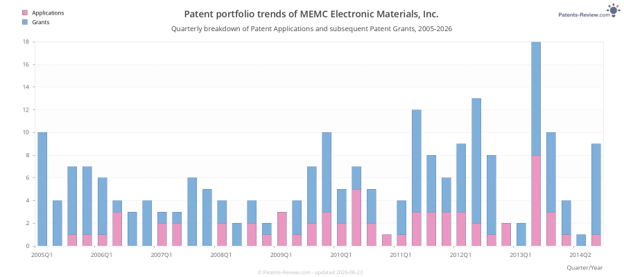
Recent patent applications by MEMC Electronic Materials, Inc.
MEMC Electronic Materials, Inc. based in St. Peters, US has been assigned the rights to these inventions. The list includes both Pending Applications and Patent Grants:
US20140273748A1
Performing operations; transportingSingle side polishing using shape matching
#2 | 2014-09-18 ✅ Patent 9,328,420 granted on 2016-05-03US20140273409A1
Chemistry; metallurgyGas distribution plate for chemical vapor deposition systems and methods of using same
#3 | 2014-08-14US20140224175A1
Chemistry; metallurgyGAS DISTRIBUTION MANIFOLD SYSTEM FOR CHEMICAL VAPOR DEPOSITION REACTORS AND METHOD OF USE
#4 | 2014-07-03 ✅ Patent 9,950,402 granted on 2018-04-24US20140183806A1
Performing operations; transportingSystem and method for aligning an ingot with mounting block
#5 | 2014-07-03 ✅ Patent 9,272,442 granted on 2016-03-01US20140182115A1
Performing operations; transportingMethods for aligning an ingot with mounting block
#6 | 2014-04-24 ✅ Patent 9,452,403 granted on 2016-09-27US20140112831A1
Performing operations; transportingUsing wavelet decomposition to determine the fluidization quality in a fluidized bed reactor
#7 | 2013-10-24 ✅ Patent 9,401,271 granted on 2016-07-26US20130276695A1
ElectricitySusceptor assemblies for supporting wafers in a reactor apparatus
#8 | 2013-10-10US20130263779A1
Chemistry; metallurgySusceptor For Improved Epitaxial Wafer Flatness
#9 | 2013-10-10 ✅ Patent 8,940,094 granted on 2015-01-27US20130263776A1
Chemistry; metallurgyMethods for fabricating a semiconductor wafer processing device
#10 | 2013-09-12 ✅ Patent 8,853,054 granted on 2014-10-07US20130237032A1
ElectricityMethod of manufacturing silicon-on-insulator wafers
#11 | 2013-09-12 ✅ Patent 9,394,180 granted on 2016-07-19US20130236367A1
Chemistry; metallurgyProduction of polycrystalline silicon in substantially closed-loop systems
#12 | 2013-08-01US20130195432A1
Mechanical engineeringTRICHLOROSILANE VAPORIZATION SYSTEM
#13 | 2013-07-11 ✅ Patent 9,317,912 granted on 2016-04-19US20130179094A1
PhysicsSymmetry based air pocket detection methods and systems
#14 | 2013-07-11 ✅ Patent 9,665,931 granted on 2017-05-30US20130176454A1
PhysicsAir pocket detection methods and systems
#15 | 2013-07-11 ✅ Patent 9,156,187 granted on 2015-10-13US20130174829A1
Performing operations; transportingMethods for mounting an ingot on a wire saw
#16 | 2013-07-11 ✅ Patent 9,061,916 granted on 2015-06-23US20130174605A1
Mechanical engineeringProcesses and systems for purifying silane
#17 | 2013-07-04US20130168836A1
ElectricitySOI STRUCTURES HAVING A SACRIFICIAL OXIDE LAYER
#18 | 2013-07-04US20130168802A1
ElectricitySOI STRUCTURES WITH REDUCED METAL CONTENT
#19 | 2013-05-30US20130137241A1
ElectricityMETHOD FOR THE PREPARATION OF A MULTI-LAYERED CRYSTALLINE STRUCTURE
#20 | 2013-05-30 ✅ Patent 9,527,752 granted on 2016-12-27US20130136686A1
Chemistry; metallurgyMethods for producing aluminum trifluoride
#21 | 2013-05-30US20130133567A1
Chemistry; metallurgySYSTEMS AND PROCESSES FOR CONTINUOUS GROWING OF INGOTS
#22 | 2013-05-30US20130133407A1
PhysicsMethods For Analysis Of Water And Substrates Rinsed In Water
#23 | 2013-05-23US20130129973A1
Chemistry; metallurgyCRUCIBLES WITH A REDUCED AMOUNT OF BUBBLES AND INGOTS AND WAFERS PRODUCED BY USE OF SUCH CRUCIBLES
#24 | 2013-05-23 ✅ Patent 8,524,319 granted on 2013-09-03US20130129921A1
Performing operations; transportingMethods for producing crucibles with a reduced amount of bubbles
#25 | 2013-05-23US20130125719A1
Chemistry; metallurgyPROCESSES FOR PRODUCING SILICON INGOTS
#26 | 2013-05-23 ✅ Patent 8,857,214 granted on 2014-10-14US20130125587A1
Chemistry; metallurgyMethods for producing crucibles with a reduced amount of bubbles
#27 | 2013-05-16 ✅ Patent 9,011,803 granted on 2015-04-21US20130121888A1
Chemistry; metallurgySystems for producing silane
#28 | 2013-05-16US20130121802A1
ElectricityWafer Transport Cart
#29 | 2013-05-16US20130118962A1
Performing operations; transportingSystems For Processing Abrasive Slurry
#30 | 2013-05-16US20130118091A1
Chemistry; metallurgyMethods For Processing Abrasive Slurry
#31 | 2013-05-02 ✅ Patent 9,159,596 granted on 2015-10-13US20130105539A1
Performing operations; transportingClamping apparatus for cleaving a bonded wafer structure
#32 | 2013-05-02 ✅ Patent 9,165,802 granted on 2015-10-20US20130105538A1
Performing operations; transportingMethods for cleaving a bonded wafer structure
#33 | 2013-04-25 ✅ Patent 8,884,310 granted on 2014-11-11US20130099195A1
ElectricityDirect formation of graphene on semiconductor substrates
#34 | 2013-04-11 ✅ Patent 8,960,657 granted on 2015-02-24US20130087132A1
Performing operations; transportingSystems and methods for connecting an ingot to a wire saw
#35 | 2013-04-04 ✅ Patent 9,114,997 granted on 2015-08-25US20130084234A1
Chemistry; metallurgyProduction of polycrystalline silicon by the thermal decomposition of silane in a fluidized bed reactor
#36 | 2013-04-04 ✅ Patent 9,114,996 granted on 2015-08-25US20130084233A1
Chemistry; metallurgyProduction of polycrystalline silicon by the thermal decomposition of silane in a fluidized bed reactor
#37 | 2013-03-14 ✅ Patent 8,845,859 granted on 2014-09-30US20130062020A1
ElectricitySystems and methods for cleaving a bonded wafer pair
#38 | 2013-01-03 ✅ Patent 8,834,825 granted on 2014-09-16US20130004405A1
Chemistry; metallurgyProcesses for producing silane in a bubble column
#39 | 2012-11-08US20120279438A1
Chemistry; metallurgyMETHODS FOR PRODUCING SINGLE CRYSTAL SILICON INGOTS WITH REDUCED INCIDENCE OF DISLOCATIONS
#40 | 2012-10-04US20120247686A1
ElectricitySystems and Methods For Ultrasonically Cleaving A Bonded Wafer Pair
#41 | 2012-09-20 ✅ Patent 8,846,493 granted on 2014-09-30US20120238070A1
ElectricityMethods for producing silicon on insulator structures having high resistivity regions in the handle wafer
#42 | 2012-09-20US20120235283A1
ElectricitySILICON ON INSULATOR STRUCTURES HAVING HIGH RESISTIVITY REGIONS IN THE HANDLE WAFER
#43 | 2012-09-13 ✅ Patent 8,728,574 granted on 2014-05-20US20120230903A1
Performing operations; transportingMethods for introducing a first gas and a second gas into a reaction chamber
#44 | 2012-08-02 ✅ Patent 8,796,116 granted on 2014-08-05US20120193753A1
ElectricityMethods for reducing the metal content in the device layer of SOI structures and SOI structures produced by such methods
#45 | 2012-07-26 ✅ Patent 8,956,584 granted on 2015-02-17US20120189527A1
Chemistry; metallurgyProduction of polycrystalline silicon in substantially closed-loop processes that involve disproportionation operations
#46 | 2012-07-26 ✅ Patent 8,715,597 granted on 2014-05-06US20120189501A1
Chemistry; metallurgyProduction of polycrystalline silicon in substantially closed-loop systems that involve disproportionation operations
#47 | 2012-07-05 ✅ Patent 8,452,547 granted on 2013-05-28US20120173170A1
PhysicsSystems and methods for particle size determination and control in a fluidized bed reactor
#48 | 2012-07-05 ✅ Patent 8,849,584 granted on 2014-09-30US20120173165A1
PhysicsSystems and methods for particle size determination and control in a fluidized bed reactor for use with thermally decomposable silicon-containing gas
#49 | 2012-06-28 ✅ Patent 9,156,705 granted on 2015-10-13US20120164323A1
Chemistry; metallurgyProduction of polycrystalline silicon by the thermal decomposition of dichlorosilane in a fluidized bed reactor
#50 | 2012-06-28 ✅ Patent 8,388,914 granted on 2013-03-05US20120164033A1
Chemistry; metallurgySystems for producing silane
#51 | 2012-06-28 ✅ Patent 8,821,825 granted on 2014-09-02US20120160702A1
Chemistry; metallurgyMethods for producing silane
#52 | 2012-05-10 ✅ Patent 8,822,242 granted on 2014-09-02US20120115258A1
ElectricityMethods for monitoring the amount of metal contamination in a process
#53 | 2012-04-26US20120100061A1
Chemistry; metallurgyProduction of Polycrystalline Silicon in Substantially Closed-loop Processes
#54 | 2012-04-26US20120100059A1
Chemistry; metallurgyProduction of Polycrystalline Silicon By The Thermal Decomposition of Trichlorosilane In A Fluidized Bed Reactor
#55 | 2012-04-26 ✅ Patent 8,449,848 granted on 2013-05-28US20120100042A1
Chemistry; metallurgyProduction of polycrystalline silicon in substantially closed-loop systems
#56 | 2012-04-10 ✅ Patent 8,153,538 granted on 2012-04-10US12964143
-Process for annealing semiconductor wafers with flat dopant depth profiles
#57 | 2012-04-05 ✅ Patent 8,524,048 granted on 2013-09-03US20120080304A1
Performing operations; transportingProcesses for recovering silane from heavy-ends separation operations
#58 | 2012-04-05 ✅ Patent 8,524,044 granted on 2013-09-03US20120080303A1
Performing operations; transportingSystems for recovering silane from heavy-ends separation operations
#59 | 2012-04-05 ✅ Patent 8,524,045 granted on 2013-09-03US20120079848A1
Chemistry; metallurgySystems for purifying silane
#60 | 2012-04-05 ✅ Patent 8,551,298 granted on 2013-10-08US20120079847A1
Chemistry; metallurgyProcesses for purifying silane
#61 | 2012-04-03 ✅ Patent 8,147,613 granted on 2012-04-03US10705813
-Crystal puller and method for growing a monocrystalline ingot
#62 | 2012-03-29 ✅ Patent 8,220,647 granted on 2012-07-17US20120077138A1
ElectricityLow thermal mass semiconductor wafer boat
#63 | 2012-03-29 ✅ Patent 8,220,646 granted on 2012-07-17US20120074081A1
ElectricityLow thermal mass semiconductor wafer plate
#64 | 2012-03-29US20120073752A1
ElectricityAdapter Ring For Silicon Electrode
#65 | 2012-02-02US20120028555A1
Performing operations; transportingGrinding Tool For Trapezoid Grinding Of A Wafer
#66 | 2012-02-02US20120028439A1
ElectricitySemiconductor And Solar Wafers And Method For Processing Same
#67 | 2012-02-02 ✅ Patent 8,528,740 granted on 2013-09-10US20120027660A1
Performing operations; transportingMethods to recover and purify silicon particles from saw kerf
#68 | 2012-02-02 ✅ Patent 8,310,031 granted on 2012-11-13US20120025353A1
ElectricitySemiconductor and solar wafers
#69 | 2012-02-02 ✅ Patent 8,505,733 granted on 2013-08-13US20120024761A1
Performing operations; transportingMethods to slice a silicon ingot
#70 | 2012-01-05 ✅ Patent 8,859,393 granted on 2014-10-14US20120003814A1
ElectricityMethods for in-situ passivation of silicon-on-insulator wafers
#71 | 2011-12-29 ✅ Patent 8,865,601 granted on 2014-10-21US20110318912A1
ElectricityMethods for preparing a semiconductor wafer with high thermal conductivity
#72 | 2011-12-08US20110300050A1
Mechanical engineeringTrichlorosilane Vaporization System
#73 | 2011-12-08US20110297861A1
Mechanical engineeringAngle Of Repose Valve
#74 | 2011-11-03 ✅ Patent 8,420,554 granted on 2013-04-16US20110269316A1
ElectricityWafer support ring
#75 | 2011-10-13US20110250739A1
ElectricityEPITAXIAL WAFER HAVING A HEAVILY DOPED SUBSTRATE AND PROCESS FOR THE PREPARATION THEREOF
#76 | 2011-10-06 ✅ Patent 8,404,206 granted on 2013-03-26US20110244124A1
Performing operations; transportingMethods for producing polycrystalline silicon that reduce the deposition of silicon on reactor walls
#77 | 2011-09-29 ✅ Patent 8,712,575 granted on 2014-04-29US20110237160A1
Performing operations; transportingHydrostatic pad pressure modulation in a simultaneous double side wafer grinder
#78 | 2011-09-15 ✅ Patent 8,735,261 granted on 2014-05-27US20110223741A1
ElectricityMethod and system for stripping the edge of a semiconductor wafer
#79 | 2011-09-01US20110212550A1
ElectricityMETHODS FOR DETECTING METAL PRECIPITATES IN A SEMICONDUCTOR WAFER
#80 | 2011-09-01US20110212547A1
ElectricityMETHODS FOR MONITORING THE AMOUNT OF METAL CONTAMINATION IMPARTED INTO WAFERS DURING A SEMICONDUCTOR PROCESS
#81 | 2011-08-25 ✅ Patent 8,440,541 granted on 2013-05-14US20110207246A1
ElectricityMethods for reducing the width of the unbonded region in SOI structures
#82 | 2011-08-25 ✅ Patent 8,330,245 granted on 2012-12-11US20110204471A1
ElectricitySemiconductor wafers with reduced roll-off and bonded and unbonded SOI structures produced from same
#83 | 2011-07-21US20110177682A1
ElectricitySUPPRESSION OF OXYGEN PRECIPITATION IN HEAVILY DOPED SINGLE CRYSTAL SILICON SUBSTRATES
#84 | 2011-07-07 ✅ Patent 9,029,854 granted on 2015-05-12US20110163313A1
ElectricityBulk silicon wafer product useful in the manufacture of three dimensional multigate MOSFETs
#85 | 2011-06-30 ✅ Patent 8,340,801 granted on 2012-12-25US20110160891A1
PhysicsSystems for generating representations of flatness defects on wafers
#86 | 2011-06-30 ✅ Patent 8,165,706 granted on 2012-04-24US20110160890A1
PhysicsMethods for generating representations of flatness defects on wafers
#87 | 2011-06-30 ✅ Patent 8,080,464 granted on 2011-12-20US20110159668A1
ElectricityMethods for processing silicon on insulator wafers
#88 | 2011-06-30 ✅ Patent 8,367,519 granted on 2013-02-05US20110159665A1
ElectricityMethod for the preparation of a multi-layered crystalline structure
#89 | 2011-06-30 ✅ Patent 8,388,925 granted on 2013-03-05US20110158896A1
Chemistry; metallurgyMethods for producing aluminum trifluoride
#90 | 2011-06-30US20110158888A1
Chemistry; metallurgyMETHODS FOR REDUCING THE DEPOSITION OF SILICON ON REACTOR WALLS USING PERIPHERAL SILICON TETRACHLORIDE
#91 | 2011-06-30 ✅ Patent 8,529,860 granted on 2013-09-10US20110158882A1
Chemistry; metallurgyMethods for producing silicon tetrafluoride
#92 | 2011-06-30 ✅ Patent 8,828,324 granted on 2014-09-09US20110158857A1
Chemistry; metallurgyFluidized bed reactor systems and distributors for use in same
#93 | 2011-06-23 ✅ Patent 8,143,078 granted on 2012-03-27US20110151592A1
ElectricityMethods for monitoring the amount of contamination imparted into semiconductor wafers during wafer processing
#94 | 2011-06-23US20110148128A1
ElectricitySemiconductor Wafer Transport System
#95 | 2011-06-23US20110146717A1
PhysicsSystems And Methods For Analysis of Water and Substrates Rinsed in Water
#96 | 2011-05-05 ✅ Patent 8,267,745 granted on 2012-09-18US20110101504A1
Performing operations; transportingMethods of grinding semiconductor wafers having improved nanotopology
#97 | 2011-02-24 ✅ Patent 8,145,342 granted on 2012-03-27US20110045740A1
Performing operations; transportingMethods and systems for adjusting operation of a wafer grinder using feedback from warp data
#98 | 2011-01-27US20110017230A1
Chemistry; metallurgyMethod and System for Processing Abrasive Slurry
#99 | 2011-01-06 ✅ Patent 8,932,550 granted on 2015-01-13US20110002835A1
Chemistry; metallurgyMethods for pulling a multicrystalline silicon ingot from a silicon melt
#100 | 2011-01-06 ✅ Patent 8,524,000 granted on 2013-09-03US20110002819A1
Chemistry; metallurgyPulling assemblies for pulling a multicrystalline silicon ingot from a silicon melt
Also check out MEMC Electronic Materials, Inc.'s (St. Peters, United States) applicant profile with 16 patent applications submitted.
1492 ⎘