Method of manufacturing a semiconductor device by using a matrix frame
US20050142814A1
2005-06-30
10/942,799
2004-09-17
✅ Patent granted
US 7,402,502 B2
2008-07-22
-
-
Chuong A. Luu
2025-03-30
Abstract:
A method of manufacturing a semiconductor device includes providing a matrix frame which includes a plurality of die pads, mounting a semiconductor chip on the respective die pads, and sealing the semiconductor chip in blocks. After the semiconductor chip is sealed by the sealing resin, inner leads which are extended from the sealing resin are punched by a punching blade. Then, the block is diced to individual semiconductor devices by a rotary blade.
Assignee:
- Oki Electric Industry Co., Ltd. 2,561 🇯🇵 Tokyo, Japan
Interested in similar patents?
Get notified when new applications in this technology area are published.
Classification:
H01L21/565 » CPC main
Processes or apparatus adapted for the manufacture or treatment of semiconductor or solid state devices or of parts thereof; Manufacture or treatment of semiconductor devices or of parts thereof the devices having at least one potential-jump barrier or surface barrier, e.g. PN junction, depletion layer or carrier concentration layer; Assembly of semiconductor devices using processes or apparatus not provided for in a single one of the subgroups - , e.g. sealing of a cap to a base of a container; Encapsulations, e.g. encapsulation layers, coatings Moulds
H01L21/4842 » CPC further
Processes or apparatus adapted for the manufacture or treatment of semiconductor or solid state devices or of parts thereof; Manufacture or treatment of semiconductor devices or of parts thereof the devices having at least one potential-jump barrier or surface barrier, e.g. PN junction, depletion layer or carrier concentration layer; Manufacture or treatment of parts, e.g. containers, prior to assembly of the devices, using processes not provided for in a single one of the subgroups -; Conductive parts; Flat leads, e.g. lead frames with or without insulating supports Mechanical treatment, e.g. punching, cutting, deforming, cold welding
H01L21/561 » CPC further
Processes or apparatus adapted for the manufacture or treatment of semiconductor or solid state devices or of parts thereof; Manufacture or treatment of semiconductor devices or of parts thereof the devices having at least one potential-jump barrier or surface barrier, e.g. PN junction, depletion layer or carrier concentration layer; Assembly of semiconductor devices using processes or apparatus not provided for in a single one of the subgroups - , e.g. sealing of a cap to a base of a container; Encapsulations, e.g. encapsulation layers, coatings Batch processing
H01L23/3107 » CPC further
Details of semiconductor or other solid state devices; Encapsulations, e.g. encapsulating layers, coatings, e.g. for protection characterised by the arrangement or shape the device being completely enclosed
H01L24/97 » CPC further
Arrangements for connecting or disconnecting semiconductor or solid-state bodies; Methods or apparatus related thereto; Batch processes at chip-level, i.e. with connecting carried out on a plurality of singulated devices, i.e. on diced chips the devices being connected to a common substrate, e.g. interposer, said common substrate being separable into individual assemblies after connecting
H01L23/49513 » CPC further
Details of semiconductor or other solid state devices; Arrangements for conducting electric current to or from the solid state body in operation, e.g. leads, terminal arrangements ; Selection of materials therefor consisting of soldered constructions; Lead-frames or other flat leads characterised by the die pad having bonding material between chip and die pad
H01L24/48 » CPC further
Arrangements for connecting or disconnecting semiconductor or solid-state bodies; Methods or apparatus related thereto; Means for bonding being attached to, or being formed on, the surface to be connected, e.g. chip-to-package, die-attach, "first-level" interconnects; Manufacturing methods related thereto; Wire connectors; Manufacturing methods related thereto; Structure, shape, material or disposition of the wire connectors after the connecting process of an individual wire connector
H01L24/73 » CPC further
Arrangements for connecting or disconnecting semiconductor or solid-state bodies; Methods or apparatus related thereto Means for bonding being of different types provided for in two or more of groups , , , , , , ,
H01L2924/01005 » CPC further
Indexing scheme for arrangements or methods for connecting or disconnecting semiconductor or solid-state bodies as covered by; Chemical elements Boron [B]
H01L2924/01006 » CPC further
Indexing scheme for arrangements or methods for connecting or disconnecting semiconductor or solid-state bodies as covered by; Chemical elements Carbon [C]
H01L2924/01029 » CPC further
Indexing scheme for arrangements or methods for connecting or disconnecting semiconductor or solid-state bodies as covered by; Chemical elements Copper [Cu]
H01L2924/01033 » CPC further
Indexing scheme for arrangements or methods for connecting or disconnecting semiconductor or solid-state bodies as covered by; Chemical elements Arsenic [As]
H01L2924/01082 » CPC further
Indexing scheme for arrangements or methods for connecting or disconnecting semiconductor or solid-state bodies as covered by; Chemical elements Lead [Pb]
H01L2224/83 » CPC further
Indexing scheme for arrangements for connecting or disconnecting semiconductor or solid-state bodies and methods related thereto as covered by; Methods for connecting semiconductor or other solid state bodies using means for bonding being attached to, or being formed on, the surface to be connected using a layer connector
H01L2224/85 » CPC further
Indexing scheme for arrangements for connecting or disconnecting semiconductor or solid-state bodies and methods related thereto as covered by; Methods for connecting semiconductor or other solid state bodies using means for bonding being attached to, or being formed on, the surface to be connected using a wire connector
H01L2224/97 » CPC further
Indexing scheme for arrangements for connecting or disconnecting semiconductor or solid-state bodies and methods related thereto as covered by; Batch processes at chip-level, i.e. with connecting carried out on a plurality of singulated devices, i.e. on diced chips the devices being connected to a common substrate, e.g. interposer, said common substrate being separable into individual assemblies after connecting
H01L2224/73265 » CPC further
Indexing scheme for arrangements for connecting or disconnecting semiconductor or solid-state bodies and methods related thereto as covered by; Means for bonding being of different types provided for in two or more of groups; Location after the connecting process on different surfaces Layer and wire connectors
H01L2924/07802 » CPC further
Indexing scheme for arrangements or methods for connecting or disconnecting semiconductor or solid-state bodies as covered by; Polymers; Adhesive characteristics other than chemical not being an ohmic electrical conductor
H01L2924/00 » CPC further
Indexing scheme for arrangements or methods for connecting or disconnecting semiconductor or solid-state bodies as covered by
H01L2924/181 » CPC further
Indexing scheme for arrangements or methods for connecting or disconnecting semiconductor or solid-state bodies as covered by; Details of package parts other than the semiconductor or other solid state devices to be connected Encapsulation
H01L2924/00012 » CPC further
Indexing scheme for arrangements or methods for connecting or disconnecting semiconductor or solid-state bodies as covered by; Technical content checked by a classifier Relevant to the scope of the group, the symbol of which is combined with the symbol of this group
H01L2224/45099 » CPC further
Indexing scheme for arrangements for connecting or disconnecting semiconductor or solid-state bodies and methods related thereto as covered by; Means for bonding being attached to, or being formed on, the surface to be connected, e.g. chip-to-package, die-attach, "first-level" interconnects; Manufacturing methods related thereto; Wire connectors; Manufacturing methods related thereto; Structure, shape, material or disposition of the wire connectors prior to the connecting process of an individual wire connector; Core members of the connector Material
H01L2924/00014 » CPC further
Indexing scheme for arrangements or methods for connecting or disconnecting semiconductor or solid-state bodies as covered by; Technical content checked by a classifier the subject-matter covered by the group, the symbol of which is combined with the symbol of this group, being disclosed without further technical details
H01L2924/207 » CPC further
Indexing scheme for arrangements or methods for connecting or disconnecting semiconductor or solid-state bodies as covered by; Parameters Diameter ranges
H01L21/46 IPC
Processes or apparatus adapted for the manufacture or treatment of semiconductor or solid state devices or of parts thereof; Manufacture or treatment of semiconductor devices or of parts thereof the devices having at least one potential-jump barrier or surface barrier, e.g. PN junction, depletion layer or carrier concentration layer the devices having semiconductor bodies not provided for in groups, , , and with or without impurities, e.g. doping materials Treatment of semiconductor bodies using processes or apparatus not provided for in groups
H01L21/78 IPC
Processes or apparatus adapted for the manufacture or treatment of semiconductor or solid state devices or of parts thereof; Manufacture or treatment of devices consisting of a plurality of solid state components formed in or on a common substrate or of parts thereof; Manufacture of integrated circuit devices or of parts thereof; Manufacture or treatment of devices consisting of a plurality of solid state components or integrated circuits formed in, or on, a common substrate with subsequent division of the substrate into plural individual devices
H01L21/30 IPC
Processes or apparatus adapted for the manufacture or treatment of semiconductor or solid state devices or of parts thereof; Manufacture or treatment of semiconductor devices or of parts thereof the devices having at least one potential-jump barrier or surface barrier, e.g. PN junction, depletion layer or carrier concentration layer the devices having semiconductor bodies comprising elements of Group IV of the Periodic System or AB compounds with or without impurities, e.g. doping materials Treatment of semiconductor bodies using processes or apparatus not provided for in groups -
H01L21/44 IPC
Processes or apparatus adapted for the manufacture or treatment of semiconductor or solid state devices or of parts thereof; Manufacture or treatment of semiconductor devices or of parts thereof the devices having at least one potential-jump barrier or surface barrier, e.g. PN junction, depletion layer or carrier concentration layer the devices having semiconductor bodies not provided for in groups, , , and with or without impurities, e.g. doping materials Manufacture of electrodes on semiconductor bodies using processes or apparatus not provided for in groups -
Description
CROSS REFERENCE TO RELATED APPLICATIONA claim of priority under 35 U.S.C. §119 is made to Japanese Patent Application No. 2003-430438, filed Dec. 25, 2003, which is herein incorporated by reference in its entirety for all purposes.
BACKGROUND OF THE INVENTION1. Field of the Invention
The present invention relates to a method of manufacturing a semiconductor device which has a sealing resin.
2. Description of the Related Art
A technique of manufacturing a semiconductor device using a matrix frame is disclosed in reference 1: Japanese Patent Laid-Open No. 2000-124239. The matrix frame which is disclosed in reference 1 includes a plurality of die pads which are arranged in a matrix. A semiconductor chip is mounted on the respective die pads. A couple of the semiconductor chips and the die pads are grouped and sealed in groups by a sealing resin. Such technique may be called a block molding method.
A reference 2: Japanese Patent Laid-Open No. 2002-43344 discloses a technique of manufacturing a semiconductor device using a matrix frame. The reference 2 discloses the following method. First, semiconductor chips are sealed in groups. Each of the groups includes a plurality of the semiconductor chips which are aligned. Then, each of the groups is separated. Finally, the sealed group is divided and individual semiconductor devices are obtained.
In the block molding method, only a peripheral area of the lead frame is clamped by a mold. Therefore, in a central area of the lead frame which is not clamped by the mold, a position of an inner lead might be moved, when a molding resin is injected in the mold.
Also, in the central area of the lead frame, a flash of the resin might be formed at a rear surface of the lead frame. It is difficult to remove the flash, and an additional step for removing the flash is needed.
Further, when the sealed block is divided by a dicing blade, a rotary speed of the dicing blade is decreased for cutting a lead frame enclosed by the sealing resin. Therefore, the dividing step requires a lot of time.
SUMMARY OF THE INVENTIONAccordingly, in one aspect of the present invention, a method of manufacturing a semiconductor device includes providing a matrix frame which includes a plurality of die pads, mounting a semiconductor chip on the respective die pads, and sealing the semiconductor chip in blocks. After the semiconductor chip is sealed by the sealing resin, inner leads which are extended from the sealing resin are punched by a punching blade. Then, the block is diced to individual semiconductor devices by a rotary blade.
BRIEF DESCRIPTION OF THE DRAWINGSFIG. 1 is a plane view showing semiconductor devices of the present invention.
FIG. 2 is a cross-sectional view showing the semiconductor devices of the present invention.
FIG. 3(A) to FIG. 3(C) are views showing the semiconductor device of the present invention.
FIG. 4 is a plane view showing a matrix frame of the present invention.
DETAILED DESCRIPTION OF THE PREFERRED EMBODIMENTSA method of manufacturing a semiconductor device according to preferred embodiments of the present invention will be explained hereinafter with reference to the accompanying figures. In order to simplify the explanation, like elements are given like or corresponding reference numerals. Dual explanations of the same elements are avoided.
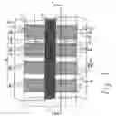
Initially, a structure of a lead frame 20 of the present invention is described by referring to FIG. 4. The lead frame 20 is made from a metal plate such as copper and has a rectangular configuration. The lead frame 20 includes a plurality of die pads 28, a frame portion 21, supporting leads 29, connecting portions 23, and inner leads 26. Each of the part including the die pads 28, supporting leads 29, connecting portion 23, and inner leads 26 are formed by a punching method or by a etching method from the metal plate.
The die pads 28 are arranged in a matrix with a distance provided between each of the die pads 28. Each of the die pads 28 has a rectangular configuration. The die pad 28 has a first side 28a and a second side 28b which are extended in a vertical direction, and a third side 28c and a fourth side 28d which are extended to a horizontal direction.
The frame portion 21 is a peripheral area of the lead frame 20. That is, the frame portion 21 surrounds the die pads 28 at a distance from the die pads 28. Sprocket holes 22 are formed in parts of the frame portion 21 which are extended in a horizontal direction. The sprocket holes 22 are used for moving the lead frame 20.
The supporting leads 29 are formed between the frame portion 21 and the die pads 28 which are located near the outside of the die pads matrix. Also, the supporting leads 29 are formed between each of the die pads 28. As a result, the die pads 28 which are aligned in the vertical direction are supported between the upper side of the frame portion 21 and the lower side of the frame portion 21 by the supporting leads 29.
The connecting portions 23 are connected between the upper side of the frame portion 21 and the lower side of the frame portion 21.
The inner leads are extended from the connecting portions 23 and the frame portion 21 to the first sides 28a and the second sides 28b of the die pads 28 so that tips of the inner leads face the first sides 28a and the second sides 28b of the die pads 28. That is, the inner leads are extended in the horizontal direction.
Supporting leads 29 are connected to the frame portion 21. In this embodiment, the supporting leads 29 have a line configuration.
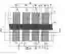
Next, a method of manufacturing the semiconductor device is described by referring to FIG. 1 and FIG. 2.
FIG. 1 is a plane view showing semiconductor devices. FIG. 2 is a cross-sectional view taken along line 2-2′ in FIG. 1. In FIG. 2, a mold is described for understanding a sealing step.
A row of the die pads 28 is used for a dummy area 34. In this embodiment, the dummy area 34 includes die pads 28 which are lined in the horizontal direction. The dummy area 34 is arranged in a middle of the die pad rows.
A semiconductor chip 42 is mounted on the respective die pads 28. In the dummy area 34, the semiconductor chip 42 is not mounted on the die pads 28. The semiconductor chip 42 includes a top surface 42a which includes a plurality of electrode pads 44 and a bottom surface 42b. The electrode pads 44 are arranged along the first side 28a and the second side 28b of the die pad 28.
In this embodiment, five rows of the die pads 28 and four columns of the die pads 28 are described in FIG. 1.
The semiconductor chip 42 is adhered on the die pad 28 by an insulating adhesive material 27 as shown in FIG. 2. Also an insulating adhesive tape can be used for the insulating adhesive material 27.
Then, the electrode pads 44 are connected to the inner leads 26 by bonding wires 46 as shown in FIG. 2. The electrode pads 44 correspond one-to-one with the inner leads 26.
Then, a sealing resin 31 is formed as shown in FIG. 2. The sealing resin 31 seals the semiconductor chips 42, the bonding wires 46, and the inner leads 26.
The sealing resin 31 is formed as block group 30. The block group 30 includes sealing resin blocks 30a. In this embodiment, each of the sealing resin blocks 30a is formed at every column of the die pads 28, and includes four semiconductor chips 42.
The sealing step is performed by setting the lead frame 20 between a mold 50 which includes an upper mold 50a and an lower mold 50b.
Cavities 52 are formed between the upper mold 50a and the lower mold 52b. Each of the die pad columns is arranged in the respective cavities 52.
Surfaces 54a of mold portions 54 which are located between cavities 52 are contacted to the connecting portion 23 and a part of the inner leads 26 of the lead frame 20, when the sealing step is performed.
A surface of the lower mold 50b is flat, and is contacted to an entire bottom surface of the lead frame 20.
After ejecting the lead frame 20 from the mold 50, a separating step is performed. In this embodiment, the separating step includes the following two steps.
A first step is a punching step by using a punching blade. A second step is a dicing step by using a rotary blade.
First, sides of the sealing resin blocks 30a are punched by the punching blade. The punching step can be performed by a punching mold which includes a plurality of the punching blades.
A rectangular or similarly shaped punching area 25 is shown by a broken line in FIG. 1. The punching blade has a rectangular punching surface which corresponds to the punching area 25. The punching blade punches the connecting portion 23 and a part of the inner leads 26. Now, a minimum width of commonly used punching blade is 3 mm to 4 mm. Therefore, a width of the connecting portion 23 should be shorter than a width of the punching blade, for punching the part of the inner leads 26.
The supporting portion 23 which is located in the dummy area 34 is not punched. That is, the punching step is performed at a first punching area 25a and a second punching area 25b which are located at both sides of the dummy area 34. After the punching step is performed, each of the sealing resin blocks 30a is connected by the supporting portions 23 which are located in the dummy area 34.
The rectangular punching area 25a and the rectangular punching area 25b can be punched simultaneously by using the punching mold. Each of the punching blades of the punching mold corresponds to the punching areas 25a and the punching areas 25b.
Then the dicing step is performed to the punched sealing resin blocks 30a, so that the respective semiconductor devices 10 are separated. The dicing step is performed by cutting the sealing blocks 30a at dicing lines L1 as shown in FIG. 1.
A width of the dummy area w2 is the same as a width of the width of the normal device area w3. As a result, the dicing step by using the rotary blade can be performed at even intervals.
In this dicing step, the sealing resin 31 and the supporting leads 29 are cut by the rotary blade. That is, the inner leads 26 are not cut by the rotary blade. Therefore, the dicing step can be performed in a short time. Also, the punching step which is performed to the inner leads 26 can inhibit a flash of the inner leads 26.
Next, the semiconductor device 10 which is manufactured by the method of this invention is described by referring to FIG. 3(A) to FIG. 3(C).
FIG. 3(A) is a schematic diagram showing the semiconductor device 10. FIG. 3(B) is a cross-sectional view taken along line 3(B)-3(B)′ in FIG. 3(A). FIG. 3(C) is a bottom view showing the semiconductor device 10.
The semiconductor device 10 includes the semiconductor chip 42. The semiconductor chip includes the top surface 42a and the bottom surface 42b. The electrode pads 44 are formed on the top surface 42a.
The semiconductor chip 42 is mounted on the die pad 28 with the adhesive material 27.
The bottom surface of the inner leads 26 which are exposed from a bottom surface 31e of the semiconductor device 10 are used as external terminals. The sealing resin 31 is remaines between the external terminals 26 as resin portions 31d.
The external terminals 26 are project from both of the side surfaces 31b of the semiconductor device 10. The external terminals 26 are arranged at even intervals.
In the side surface 31c of the semiconductor device 10, a cutting surface of the supporting lead 29 is exposed as shown in FIG. 3(A).
While the preferred form of the present invention has been described, it is to be understood that modifications will be apparent to those skilled in the art without departing from the spirit of the invention. The scope of the invention is to be determined solely by the following claims.
Claims
1. A method of manufacturing a semiconductor device comprising:
providing a matrix frame which includes a plurality of die pads each of which is arranged along a plurality of rows and a plurality of columns, a plurality of inner leads which are arranged along sides of the die pads in a row direction, and a plurality of supporting leads which support the die pad from the column direction;
mounting a semiconductor chips on the respective die pads;
sealing the semiconductor chips by a sealing resin in blocks, wherein each of the blocks includes a plurality of semiconductor chips;
punching an area which surrounds the respective blocks with a punching blade; and
dicing the blocks into individual semiconductor devices with a rotary blade.
2. The method of claim 1, wherein each of the blocks corresponds to the respective columns.
3. The method of claim 1, wherein the matrix frame includes connecting portions which are arranged in the column direction, and wherein the inner leads extend from the connection portions.
4. The method of claim 1, wherein the inner leads are cut by said punching, and the supporting leads are cut by said dicing.
5. The method of claim 3, wherein the connection portions and the inner leads are cut by said punching simultaneously.
6. A method of manufacturing a semiconductor device comprising:
providing a matrix frame which includes a frame portion which is arranged in a peripheral area of the matrix frame, a plurality of die pad groups each of which includes a plurality of die pads and a dummy pad which are arranged along a line, supporting leads which support the respective die pads, connecting portions which are arranged between respective die pad groups, and inner leads which are connected to the connecting portions;
mounting semiconductor chips on the respective die pads;
sealing the die pads, the semiconductor chips, the inner leads, and the supporting leads by a sealing resin;
punching the connecting portions and the inner leads which are arranged between the die pads with a punching blade, wherein the inner leads and the connecting portions which are arranged between the respective dummy pads are not punched; and
dicing the supporting leads and the resin between the respective die pads with a rotary blade.
7. The method of claim 6, wherein each of the dummy pads is arranged in a middle area of the respective die pad groups.
8. The method of claim 7, wherein the inner leads and the connecting portions which are separated by the dummy pads are punched simultaneously.
9. A method of manufacturing a semiconductor device comprising:
providing a matrix frame which includes a plurality of die pads which are arranged in a matrix, supporting leads, and inner leads;
mounting semiconductor chips on the respective die pads;
sealing the semiconductor chips with a sealing resin in groups, wherein the inner leads extend from the sealing resin;
punching the inner leads with a punching blade; and
dicing the supporting leads and the sealing resin which are arranged between respective die pads with a rotary blade.
Images & Drawings included:


Sources:
- United States Patent and Trademark Office - verify current appl. status at the USPTO↗
Recent applications in this class:
- » 20250279288 2025-09-04
PACKAGE STRUCTURE INCLUDING PHOTONIC PACKAGE HAVING EMBEDDED OPTICAL GLUE - » 20250246446 2025-07-31
SEMICONDUCTOR MODULE AND MANUFACTURING METHOD THEREOF - » 20250218800 2025-07-03
SEMICONDUCTOR DEVICE, SEMICONDUCTOR PACKAGE, AND PRINTED CIRCUIT BOARD HAVING A PATTERN - » 20250183058 2025-06-05
CROSS-WAFER RDLS IN CONSTRUCTED WAFERS - » 20250157829 2025-05-15
SEMICONDUCTOR DEVICE FABRICATION METHOD AND LEAD FRAME WITH SIDE PORTION MOLD LOCKING STRUCTURE - » 20250149348 2025-05-08
METHOD FOR REDUCING WARPAGE OCCURRED TO SUBSTRATE DURING PACKAGING PROCESS - » 20250140574 2025-05-01
HYBRID MOLD CHASE SURFACE FOR SEMICONDUCTOR BONDING AND RELATED SYSTEMS AND METHODS - » 20250125158 2025-04-17
METHOD FOR ATTACHING A HEAT SPREADER TO A SEMICONDUCTOR PACKAGE AND SEMICONDUCTOR PACKAGE ASSEMBLIES - » 20250112058 2025-04-03
METHOD FOR DECAPSULATING PACKAGED INTEGRATED CIRCUIT - » 20250062138 2025-02-20
PACKAGE STRUCTURE AND METHOD FOR FABRICATING THE SAME
Recent applications for this Assignee:
- » 20250277907 2025-09-04
INFORMATION PROCESSING DEVICE, INFORMATION PROCESSING METHOD, AND NON-TRANSITORY COMPUTER READABLE STORAGE MEDIUM - » 20250274548 2025-08-28
MANAGEMENT APPARATUS, SYSTEM, AND INFORMATION PROCESSING METHOD - » 20250271810 2025-08-28
MEDIUM TRANSPORT APPARATUS - » 20250241046 2025-07-24
SEMICONDUCTOR ELEMENT UNIT AND METHOD OF MANUFACTURING THEREOF, SEMICONDUCTOR ELEMENT UNIT SUPPLY SUBSTRATE, AND SEMICONDUCTOR PACKAGING CIRCUIT AND METHOD OF MANUFACTURING THEREOF - » 20250148495 2025-05-08
BEHAVIOR CHANGE INTERVENTION SYSTEM, BEHAVIOR CHANGE INTERVENTION METHOD, AND NON-TRANSITORY COMPUTER READABLE STORAGE MEDIUM - » 20250098998 2025-03-27
PSYCHOLOGICAL STATE ESTIMATION SYSTEM, PSYCHOLOGICAL STATE ESTIMATION METHOD, NON-TRANSITORY COMPUTER READABLE STORAGE MEDIUM - » 20250096217 2025-03-20
METHOD OF MANUFACTURING SEMICONDUCTOR COMPOSITE DEVICE - » 20250076779 2025-03-06
DRUM UNIT AND IMAGE FORMATION APPARATUS - » 20250076103 2025-03-06
LASER DOPPLER VIBROMETER AND VIBRATION MEASUREMENT METHOD - » 20250068098 2025-02-27
IMAGE FORMING DEVICE AND IMAGE FORMING METHOD