Semiconductor package with wire bond arrangement to reduce cross talk for high speed circuits
US20060065983A1
2006-03-30
10/956,656
2004-09-30
Abstract:
A package for reducing signal cross talk between wire bonds of semiconductor packages. The package includes a semiconductor die having a plurality of bond pads formed thereon. The bond pads arranged in a first subset of bond pads and a second subset of bond pads. The package also includes a substrate having a plurality of contact points, the plurality of contact points are arranged in a first subset of contact points and a second subset of contact points. To reduce signal cross talk, the wire bonds are arranged such that a first subset of wire bonds are electrically coupled between the first subset of bond pads and the first subset of the contact points. The first subset of wire bonds have ball bonds formed on the first subset of bond pads and stitch bonds formed on the first subset of contact points respectively. A second subset of wire bonds are electrically coupled between the second subset of bond pads and the second subset of the contact points. The second subset of wire bonds have stitch bonds formed on the first subset of bond pads and ball bonds formed on the first subset of contact points respectively. The different height profiles of the first set and the second set of wire bonds tends to reduce signal cross talk between the wires.
Inventors:
- Chok J. Chia 14 🇺🇸 Cupertino, CA, United States
- Seng-sooi Lim 2 🇺🇸 San Jose, CA, United States
- Wee Keong Liew 2 🇺🇸 San Jose, CA, United States
Assignee:
- LSI LOGIC CORPORATION 436 🇺🇸 Milpitas, CA, United States
Interested in similar patents?
Get notified when new applications in this technology area are published.
Classification:
H01L2924/00012 » CPC further
Indexing scheme for arrangements or methods for connecting or disconnecting semiconductor or solid-state bodies as covered by; Technical content checked by a classifier Relevant to the scope of the group, the symbol of which is combined with the symbol of this group
H01L23/52 IPC
Details of semiconductor or other solid state devices Arrangements for conducting electric current within the device in operation from one component to another, i.e. interconnections, e.g. wires, lead frames
H01L24/85 » CPC main
Arrangements for connecting or disconnecting semiconductor or solid-state bodies; Methods or apparatus related thereto; Methods for connecting semiconductor or other solid state bodies using means for bonding being attached to, or being formed on, the surface to be connected using a wire connector
H01L24/49 » CPC further
Arrangements for connecting or disconnecting semiconductor or solid-state bodies; Methods or apparatus related thereto; Means for bonding being attached to, or being formed on, the surface to be connected, e.g. chip-to-package, die-attach, "first-level" interconnects; Manufacturing methods related thereto; Wire connectors; Manufacturing methods related thereto; Structure, shape, material or disposition of the wire connectors after the connecting process of a plurality of wire connectors
H01L23/49838 » CPC further
Details of semiconductor or other solid state devices; Arrangements for conducting electric current to or from the solid state body in operation, e.g. leads, terminal arrangements ; Selection of materials therefor consisting of soldered constructions; Leads, on insulating substrates, Geometry or layout
H01L24/48 » CPC further
Arrangements for connecting or disconnecting semiconductor or solid-state bodies; Methods or apparatus related thereto; Means for bonding being attached to, or being formed on, the surface to be connected, e.g. chip-to-package, die-attach, "first-level" interconnects; Manufacturing methods related thereto; Wire connectors; Manufacturing methods related thereto; Structure, shape, material or disposition of the wire connectors after the connecting process of an individual wire connector
H01L24/73 » CPC further
Arrangements for connecting or disconnecting semiconductor or solid-state bodies; Methods or apparatus related thereto Means for bonding being of different types provided for in two or more of groups , , , , , , ,
H01L2223/6611 » CPC further
Details relating to semiconductor or other solid state devices covered by the group; Structural electrical arrangements for semiconductor devices not otherwise provided for; Impedance arrangements; High-frequency adaptations; High-frequency electrical connections Wire connections
H01L2224/4943 » CPC further
Indexing scheme for arrangements for connecting or disconnecting semiconductor or solid-state bodies and methods related thereto as covered by; Means for bonding being attached to, or being formed on, the surface to be connected, e.g. chip-to-package, die-attach, "first-level" interconnects; Manufacturing methods related thereto; Wire connectors; Manufacturing methods related thereto; Structure, shape, material or disposition of the wire connectors after the connecting process of a plurality of wire connectors; Connecting portions the connecting portions being staggered
H01L2924/01029 » CPC further
Indexing scheme for arrangements or methods for connecting or disconnecting semiconductor or solid-state bodies as covered by; Chemical elements Copper [Cu]
H01L2924/01033 » CPC further
Indexing scheme for arrangements or methods for connecting or disconnecting semiconductor or solid-state bodies as covered by; Chemical elements Arsenic [As]
H01L2924/01082 » CPC further
Indexing scheme for arrangements or methods for connecting or disconnecting semiconductor or solid-state bodies as covered by; Chemical elements Lead [Pb]
H01L2924/014 » CPC further
Indexing scheme for arrangements or methods for connecting or disconnecting semiconductor or solid-state bodies as covered by; Alloys Solder alloys
H01L2924/3025 » CPC further
Indexing scheme for arrangements or methods for connecting or disconnecting semiconductor or solid-state bodies as covered by; Technical effects; Electrical effects Electromagnetic shielding
H01L2224/78 » CPC further
Indexing scheme for arrangements for connecting or disconnecting semiconductor or solid-state bodies and methods related thereto as covered by; Apparatus for manufacturing arrangements for connecting or disconnecting semiconductor or solid-state bodies and for methods related thereto Apparatus for connecting with wire connectors
H01L2224/4945 » CPC further
Indexing scheme for arrangements for connecting or disconnecting semiconductor or solid-state bodies and methods related thereto as covered by; Means for bonding being attached to, or being formed on, the surface to be connected, e.g. chip-to-package, die-attach, "first-level" interconnects; Manufacturing methods related thereto; Wire connectors; Manufacturing methods related thereto; Structure, shape, material or disposition of the wire connectors after the connecting process of a plurality of wire connectors; Connecting portions Wire connectors having connecting portions of different types on the semiconductor or solid-state body, e.g. regular and reverse stitches
H01L2924/00 » CPC further
Indexing scheme for arrangements or methods for connecting or disconnecting semiconductor or solid-state bodies as covered by
H01L2924/15311 » CPC further
Indexing scheme for arrangements or methods for connecting or disconnecting semiconductor or solid-state bodies as covered by; Details of package parts other than the semiconductor or other solid state devices to be connected; Die mounting substrate; Connection portion the connection portion being formed only on the surface of the substrate opposite to the die mounting surface being a ball array, e.g. BGA
H01L2224/73265 » CPC further
Indexing scheme for arrangements for connecting or disconnecting semiconductor or solid-state bodies and methods related thereto as covered by; Means for bonding being of different types provided for in two or more of groups; Location after the connecting process on different surfaces Layer and wire connectors
H01L2224/45099 » CPC further
Indexing scheme for arrangements for connecting or disconnecting semiconductor or solid-state bodies and methods related thereto as covered by; Means for bonding being attached to, or being formed on, the surface to be connected, e.g. chip-to-package, die-attach, "first-level" interconnects; Manufacturing methods related thereto; Wire connectors; Manufacturing methods related thereto; Structure, shape, material or disposition of the wire connectors prior to the connecting process of an individual wire connector; Core members of the connector Material
H01L2924/00014 » CPC further
Indexing scheme for arrangements or methods for connecting or disconnecting semiconductor or solid-state bodies as covered by; Technical content checked by a classifier the subject-matter covered by the group, the symbol of which is combined with the symbol of this group, being disclosed without further technical details
H01L2224/05599 » CPC further
Indexing scheme for arrangements for connecting or disconnecting semiconductor or solid-state bodies and methods related thereto as covered by; Means for bonding being attached to, or being formed on, the surface to be connected, e.g. chip-to-package, die-attach, "first-level" interconnects; Manufacturing methods related thereto; Bonding areas; Manufacturing methods related thereto; Structure, shape, material or disposition of the bonding areas prior to the connecting process of an individual bonding area; External layer Material
H01L2924/181 » CPC further
Indexing scheme for arrangements or methods for connecting or disconnecting semiconductor or solid-state bodies as covered by; Details of package parts other than the semiconductor or other solid state devices to be connected Encapsulation
Description
BACKGROUND OF THE INVENTION1. Field of the Invention
The present invention relates generally to semiconductor packaging, and more particularly, to a semiconductor package with a wire bond arrangement to reduce cross talk between the wires.
2. Description of the Related Art
Advances in processing technology has allowed engineers to fabricate smaller and smaller transistors. The smaller transistors not only operate at faster speeds, but they also enable more and more transistors to be fabricated on a semiconductor die of a given size. This increased circuit density has enabled circuit designers to add greater functionality with each new generation of chips. The new functionality, however, increases the need for a greater number of signal inputs as well as power and ground inputs to the device. State of the art chip packages currently have hundreds and in some instances thousands of input-output pins. The increased number of input-output pins results in the bond pads on the die and the bond fingers or leads of the leadframe package to have a finer pitch. Consequently, wire bonds are spaced very close to one another on the packaged die. The closeness of the wires may create a problem. Namely, coupling noise and cross talk between the wires may cause false signal transitions on the signal input-output pins, causing the device to fail. The faster switching speeds of the transistors further exasperates this problem.
A number of approaches are known to reduce the coupling noise and cross talk problem with wire bonds of semiconductor packages. One conventional approach is to use wire bonds of different heights and loop profiles to reduce the cross talk and coupling noise between the wires. Another technique is to convert a significant number of signal bond pads into either ground (VSS) or power (VDD) pads. The spacing of either VSS or VDD pads between signal pads provides electrical shielding, isolating the adjacent signal and clock wires from coupling noise and cross talk. The problem with this approach is that it reduces the total number of usable signal input-output pins on the package.
Accordingly, there is a need for a semiconductor package with a wire bond arrangement to reduce cross talk between the wires.
SUMMARY OF THE INVENTIONThe present invention relates to a semiconductor package for reducing signal cross talk between wire bonds of a semiconductor packages. The package includes a semiconductor die having a plurality of bond pads formed thereon. The bond pads are arranged in a first subset of bond pads and a second subset of bond pads. The package also includes a substrate having a plurality of contact points, the plurality of contact points are arranged in a first subset of contact points and a second subset of contact points. To reduce signal cross talk, the wire bonds are arranged such that a first subset of wire bonds are electrically coupled between the first subset of bond pads and the first subset of the contact points. The first subset of wire bonds have ball bonds formed on the first subset of bond pads and stitch bonds formed on the first subset of contact points respectively. A second subset of wire bonds are electrically coupled between the second subset of bond pads and the second subset of the contact points. The second subset of wire bonds have stitch bonds formed on the first subset of bond pads and ball bonds formed on the first subset of contact points respectively. The different height profiles of the first set and the second set of wire bonds tends to reduce signal cross talk between the wires.
BRIEF DESCRIPTION OF THE DRAWINGSThe invention, together with further advantages thereof, may best be understood by reference to the following description taken in conjunction with the accompanying drawings in which:
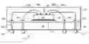
FIG. 1 is a cross section of a semiconductor package of the present invention.
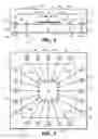
FIG. 2 is a top view of the semiconductor package of the present invention.
In the figures, like reference numbers refer to like components and elements.
DETAILED DESCRIPTION OF THE INVENTIONReferring to FIG. 1, a cross section of a package of the present invention is shown. The package 10 includes a semiconductor die 12 mounted onto a die attach area 14 of a substrate 16. A die attach material 18, such as an epoxy, is used to attach the die 12 to the die attach area 14. A plurality of solder ball contacts 20 are formed on the bottom surface of the substrate 16. The solder ball contacts 20 are electrically coupled to a plurality of contact points 22 on the top surface of the substrate 16 through vias 24. Although not visible in FIG. 1, the die 12 has a plurality of bond pads formed on the upper or active surface. Wire bonds 26 are formed between the bond pads on the die 12 and the contact points 22 on the substrate 16. The package is encapsulated in an encapsulant material 27.
In accordance with the present invention, the wire bonds 26 are arranged in a first subset 26a and a second subset 26b.
-
- 1. The bond wires 26a of the first subset are electrically coupled between a first set of bond pads on the die 12 and a first set of contact points 22 on the substrate 16 respectively. The first subset of wire bonds 26a are formed by ball bonds 28 formed on the first subset of bond pads on the die 12 and stitch bonds 30 formed on the first subset of contact points 22 respectively. The ball bonds are designated by an “•” and the stitch bonds are designated by an “x” in the figures.
- 2. Alternatively, the second subset of bond wires 26b of the selected subject are electrically coupled between a second set of bond pads on the die 12 and a second set of contact points 22 on the substrate 16. The second subset of wire bonds 26b are formed by stitch bonds 30 formed on the second subset of bond pads on the die 12 and ball bonds 28 formed on the second subset of contact points 22 on the substrate 16 respectively. Again, the ball bonds are designated by an “•” and the stitch bonds are designated by an “x” in the figures
As is evident in FIG. 1, the first set of wire bonds 26a and the second set of wire bonds 26b have different height profiles. The height profile of the first set of wire bonds 26a are higher relative to the second set of wire bonds 26b. The different height profile tends to reduce signal noise and cross talk between the bond wires 26.
Referring to FIG. 2, a top view of the package 10 is shown. In this view, the die 12 is shown mounted onto the die attach area (not visible) in the center and the plurality of contact points 22 are arranged around the periphery of the substrate 16. In one embodiment, the individual wire bonds of the first subset of wire bond 26a and the second subset of wire bonds 26b are arranged adjacent to one another respectively. In other words, each bond wire 26a is “sandwiched” between two adjacent bond wires 26b and vice versa. Again, the different height profiles of the adjacent wire bonds 26 tends to reduce signal noise and cross talk between the wires.
Although the foregoing invention has been described in some detail for purposes of clarity of understanding, it will be apparent that certain changes and modifications may be practiced within the scope of the appended claims. For example, the substrate 14 and described herein can be made of a number of different materials, such as ceramic or plastic. The substrate 14 can also be a lead frame made of a metal such as copper. In embodiments where the substrate 16 is a lead frame, the die 12 is attached to the die attach pad and the contact pads 22 are leads of the lead frame. Therefore, the described embodiments should be taken as illustrative and not restrictive, and the invention should not be limited to the details given herein but should be defined by the following claims and their full scope of equivalents.
Claims
We claim:1. An semiconductor package, comprising;
a semiconductor die having a plurality of bond pads formed thereon, the bond pads arranged in a first subset of bond pads and a second subset of bond pads;
a substrate having a die attach area and a plurality of contact points, the plurality of contact points arranged in a first subset of contact points and a second subset of contact points;
a first subset of wire bonds electrically coupled between the first subset of bond pads and the first subset of the contact points, the first subset of wire bonds having ball bonds formed on the first subset of bond pads and stitch bonds formed on the first subset of contact points respectively; and
a second subset of wire bonds electrically coupled between the second subset of bond pads and the second subset of the contact points, the second subset of wire bonds having stitch bonds formed on the first subset of bond pads and ball bonds formed on the first subset of contact points respectively.
2. The package of claim 1, wherein the first subset of wire bonds has a first height profile.
3. The package of claim 2, wherein the second subset of wire bonds has a second height profile, the first height profile being different than the second height profile.
4. The package of claim 1, wherein the height profile of the first subset of wire bonds is higher relative to the height profile of the second subset of wire bonds.
5. The package of claim 1, wherein individual wire bonds of the first subset of wire bond and the second subset of wire bonds are arranged adjacent to one another respectively.
6. The package of claim 1, wherein individual wire bonds of the first subset of wire bond and the second subset of wire bonds are arranged in an alternating pattern respectively.
7. The package of claim 1, wherein the substrate is a lead frame and the contact points are leads on the lead frame.
8. A method of making a semiconductor package, comprising;
providing a die on a die attach area of a substrate,
the die having a plurality of bond pads formed thereon, the bond pads arranged in a first subset of bond pads and a second subset of bond pads; and
the substrate having a plurality of contact points, the plurality of contact points arranged in a first subset of contact points and a second subset of contact points;
forming a first subset of wire bonds electrically coupled between the first subset of bond pads and the first subset of the contact points, the first subset of wire bonds formed by:
forming ball bonds on the first subset of bond pads; and
forming stitch bonds on the first subset of contact points respectively; and
forming a second subset of wire bonds electrically coupled between the second subset of bond pads and the second subset of the contact points, the second subset of wire bonds formed by:
forming stitch bonds on the second subset of bond pads; and
forming ball bonds on the first subset of contact points respectively.
9. The method of claim 8, wherein the first subset of wire bonds has a first height profile.
10. The method of claim 9, wherein the second subset of wire bonds has a second height profile, the first height profile being different than the second height profile.
11. The method of claim 8, wherein the height profile of the first subset of wire bonds is higher relative to the height profile of the second subset of wire bonds.
12. The method of claim 8, further arranging the individual wire bonds of the first subset of wire bond and the second subset of wire bonds in an alternating pattern respectively.
13. The method of claim 8, wherein the substrate is a lead frame and the contact points are leads on the lead frame.
Images & Drawings included:
Sources:
- United States Patent and Trademark Office - verify current appl. status at the USPTO↗
Recent applications in this class:
- » 20250149502 2025-05-08
CAPILLARY FOR A WIRE BONDING MACHINE HAVING A DYNAMICALLY ADJUSTABLE CHAMFER DIAMETER - » 20250140740 2025-05-01
METHOD OF MANUFACTURING SEMICONDUCTOR DEVICE - » 20250140739 2025-05-01
LASER ENHANCED WIRE BONDING FOR SEMICONDUCTOR DEVICE PACKAGES - » 20250125305 2025-04-17
METHOD OF MANUFACTURING SEMICONDUCTOR DEVICE WITH FIXING FEATURE ON WHICH BONDING WIRE IS DISPOSED - » 20250118705 2025-04-10
PACKAGE-ON-PACKAGE ASSEMBLY WITH WIRE BOND VIAS - » 20250118704 2025-04-10
APPARATUS AND METHODS FOR TOOL MARK FREE STITCH BONDING - » 20250096195 2025-03-20
Wire Bonding Method and Apparatus - » 20250079396 2025-03-06
METHODS OF DETERMINING A SEQUENCE FOR CREATING A PLURALITY OF WIRE LOOPS IN CONNECTION WITH A WORKPIECE - » 20250070081 2025-02-27
METHOD FOR FORMING AN ELECTRICAL CONNECTION BETWEEN AN ELECTRONIC CHIP AND A CARRIER SUBSTRATE AND ELECTRONIC DEVICE - » 20240363583 2024-10-31
Methods of forming wire interconnect structures and related wire bonding tools
Recent applications for this Assignee:
- » 20100200993 2010-08-12
Dielectric barrier layer for increasing electromigration lifetimes in copper interconnect structures - » 20100097875 2010-04-22
Enhanced power distribution in an integrated circuit - » 20100067207 2010-03-18
Semiconductor package and method using isolated Vplane to accommodate high speed circuitry ground isolation - » 20100042966 2010-02-18
Synthesized logic replacement - » 20100037448 2010-02-18
Adjustable EMI baffling method for data storage systems - » 20100002526 2010-01-07
Latch-based random access memory - » 20090323870 2009-12-31
Identification circuit with repeatable output code - » 20090283904 2009-11-19
Flipchip bump patterns for efficient I-mesh power distribution schemes - » 20090256217 2009-10-15
CARBON NANOTUBE MEMORY CELLS HAVING FLAT BOTTOM ELECTRODE CONTACT SURFACE - » 20090125769 2009-05-14
On-chip circuit for transition delay fault test pattern generation with launch off shift