Hybrid card
US20060104041A1
2006-05-18
10/528,306
2003-09-17
✅ Patent granted
US 7,387,259 B2
2008-06-17
WO; PCT/IB03/04011; 20030917
WO; WO2004/027863; 20040401
Michael G. Lee | Tae W Kim
2023-09-17
Abstract:
A card like object comprises a card body comprising a first face. The first face is at least partially graphically personalized. An antenna is embedded in the card body. The card body is provided with a cavity. The cavity comprises a contact chip. The cavity further comprises a contactless chip, the contactless chip being electrically connected to the antenna with connecting means.
Assignee:
- AXALTO SA 34 🇫🇷 Montrouge, France
Interested in similar patents?
Get notified when new applications in this technology area are published.
Classification:
G06K19/07747 » CPC main
Record carriers for use with machines and with at least a part designed to carry digital markings characterised by the kind of the digital marking, e.g. shape, nature, code; Record carriers with conductive marks, printed circuits or semiconductor circuit elements, e.g. credit or identity cards also with resonating or responding marks without active components with integrated circuit chips; Constructional details, e.g. mounting of circuits in the carrier; Mounting details of integrated circuit chips at least one of the integrated circuit chips being mounted as a module
G06K19/072 » CPC further
Record carriers for use with machines and with at least a part designed to carry digital markings characterised by the kind of the digital marking, e.g. shape, nature, code; Record carriers with conductive marks, printed circuits or semiconductor circuit elements, e.g. credit or identity cards also with resonating or responding marks without active components with integrated circuit chips the record carrier comprising a plurality of integrated circuit chips
G06K19/077 » CPC further
Record carriers for use with machines and with at least a part designed to carry digital markings characterised by the kind of the digital marking, e.g. shape, nature, code; Record carriers with conductive marks, printed circuits or semiconductor circuit elements, e.g. credit or identity cards also with resonating or responding marks without active components with integrated circuit chips Constructional details, e.g. mounting of circuits in the carrier
G06K19/07745 » CPC further
Record carriers for use with machines and with at least a part designed to carry digital markings characterised by the kind of the digital marking, e.g. shape, nature, code; Record carriers with conductive marks, printed circuits or semiconductor circuit elements, e.g. credit or identity cards also with resonating or responding marks without active components with integrated circuit chips; Constructional details, e.g. mounting of circuits in the carrier Mounting details of integrated circuit chips
G06K19/07749 » CPC further
Record carriers for use with machines and with at least a part designed to carry digital markings characterised by the kind of the digital marking, e.g. shape, nature, code; Record carriers with conductive marks, printed circuits or semiconductor circuit elements, e.g. credit or identity cards also with resonating or responding marks without active components with integrated circuit chips; Constructional details, e.g. mounting of circuits in the carrier the record carrier being capable of non-contact communication, e.g. constructional details of the antenna of a non-contact smart card
G06K19/0775 » CPC further
Record carriers for use with machines and with at least a part designed to carry digital markings characterised by the kind of the digital marking, e.g. shape, nature, code; Record carriers with conductive marks, printed circuits or semiconductor circuit elements, e.g. credit or identity cards also with resonating or responding marks without active components with integrated circuit chips; Constructional details, e.g. mounting of circuits in the carrier the record carrier being capable of non-contact communication, e.g. constructional details of the antenna of a non-contact smart card arrangements for connecting the integrated circuit to the antenna
H01L21/50 » CPC further
Processes or apparatus adapted for the manufacture or treatment of semiconductor or solid state devices or of parts thereof; Manufacture or treatment of semiconductor devices or of parts thereof the devices having at least one potential-jump barrier or surface barrier, e.g. PN junction, depletion layer or carrier concentration layer Assembly of semiconductor devices using processes or apparatus not provided for in a single one of the subgroups - , e.g. sealing of a cap to a base of a container
H01L23/49855 » CPC further
Details of semiconductor or other solid state devices; Arrangements for conducting electric current to or from the solid state body in operation, e.g. leads, terminal arrangements ; Selection of materials therefor consisting of soldered constructions; Leads, on insulating substrates, for flat-cards, e.g. credit cards
H01L24/45 » CPC further
Arrangements for connecting or disconnecting semiconductor or solid-state bodies; Methods or apparatus related thereto; Means for bonding being attached to, or being formed on, the surface to be connected, e.g. chip-to-package, die-attach, "first-level" interconnects; Manufacturing methods related thereto; Wire connectors; Manufacturing methods related thereto; Structure, shape, material or disposition of the wire connectors prior to the connecting process of an individual wire connector
H01L24/48 » CPC further
Arrangements for connecting or disconnecting semiconductor or solid-state bodies; Methods or apparatus related thereto; Means for bonding being attached to, or being formed on, the surface to be connected, e.g. chip-to-package, die-attach, "first-level" interconnects; Manufacturing methods related thereto; Wire connectors; Manufacturing methods related thereto; Structure, shape, material or disposition of the wire connectors after the connecting process of an individual wire connector
H01L2224/73265 » CPC further
Indexing scheme for arrangements for connecting or disconnecting semiconductor or solid-state bodies and methods related thereto as covered by; Means for bonding being of different types provided for in two or more of groups; Location after the connecting process on different surfaces Layer and wire connectors
H01L2924/01055 » CPC further
Indexing scheme for arrangements or methods for connecting or disconnecting semiconductor or solid-state bodies as covered by; Chemical elements Cesium [Cs]
H01L2224/45099 » CPC further
Indexing scheme for arrangements for connecting or disconnecting semiconductor or solid-state bodies and methods related thereto as covered by; Means for bonding being attached to, or being formed on, the surface to be connected, e.g. chip-to-package, die-attach, "first-level" interconnects; Manufacturing methods related thereto; Wire connectors; Manufacturing methods related thereto; Structure, shape, material or disposition of the wire connectors prior to the connecting process of an individual wire connector; Core members of the connector Material
H01L2224/05599 » CPC further
Indexing scheme for arrangements for connecting or disconnecting semiconductor or solid-state bodies and methods related thereto as covered by; Means for bonding being attached to, or being formed on, the surface to be connected, e.g. chip-to-package, die-attach, "first-level" interconnects; Manufacturing methods related thereto; Bonding areas; Manufacturing methods related thereto; Structure, shape, material or disposition of the bonding areas prior to the connecting process of an individual bonding area; External layer Material
H01L2924/00014 » CPC further
Indexing scheme for arrangements or methods for connecting or disconnecting semiconductor or solid-state bodies as covered by; Technical content checked by a classifier the subject-matter covered by the group, the symbol of which is combined with the symbol of this group, being disclosed without further technical details
H01L2924/14 » CPC further
Indexing scheme for arrangements or methods for connecting or disconnecting semiconductor or solid-state bodies as covered by; Details of semiconductor or other solid state devices to be connected; Device type Integrated circuits
H01L2924/00 » CPC further
Indexing scheme for arrangements or methods for connecting or disconnecting semiconductor or solid-state bodies as covered by
H01L2924/181 » CPC further
Indexing scheme for arrangements or methods for connecting or disconnecting semiconductor or solid-state bodies as covered by; Details of package parts other than the semiconductor or other solid state devices to be connected Encapsulation
H01L2924/00012 » CPC further
Indexing scheme for arrangements or methods for connecting or disconnecting semiconductor or solid-state bodies as covered by; Technical content checked by a classifier Relevant to the scope of the group, the symbol of which is combined with the symbol of this group
H05K7/08 IPC
Constructional details common to different types of electric apparatus; Arrangements of circuit components or wiring on supporting structure on insulating boards, e.g. wiring harnesses on perforated boards
H05K7/08 IPC
Constructional details common to different types of electric apparatus; Arrangements of circuit components or wiring on supporting structure on insulating boards, e.g. wiring harnesses on perforated boards
G06K19/06 IPC
Record carriers for use with machines and with at least a part designed to carry digital markings characterised by the kind of the digital marking, e.g. shape, nature, code
Description
FIELD OF THE INVENTIONThe invention concerns hybrid cards. “Hybrid cards” stands here for cards including a chip with its ISO 7816 contact interface and a second chip with its ISO 14443 contactless interface.
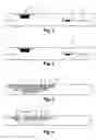
BACKGROUND OF THE INVENTIONGenerally hybrid cards are graphically personalized on their surface by means of, for example, dye thermal transfer printers. As illustrated in FIG. 1, conventional hybrid cards comprise a contactless chip and a contact chip.
The contactless chip (1) is connected to an antenna (2), either directly by means of the flip-chip technology, or indirectly if it is encapsuled into a module that is connected to the antenna by means of either welding, brazing or conductive adhesive based technologies. The antenna is a set of loops that may be either constituted of wound wires, either printed by way of additive or subtractive processes. The antenna and the contactless chip or contactless module are embedded in the card body (3).
The contact chip is connected to contact areas located as defined in the ISO 7816 standard. This chip is most generally encapsuled in a module (4).
SUMMARY OF THE INVENTIONAn object of the invention is to both allow reducing of the costs and to obtain hybrid cards with an enhanced quality.
According to one aspect of the invention, a card like object comprising a card body comprising a first face, the first face being at least partially graphically personalized, an antenna being embedded in the card body, the card body being provided with a cavity, the cavity comprising a contact chip, is characterized in that the cavity further comprises a contactless chip, the contactless chip being electrically connected to the antenna with connecting means.
Conventional hybrid card manufacturing technologies do not fully comply with dye thermal transfer printing process due to the surface unevenness defect induced by the contactless chip or contactless module located in the thickness of the card body.
As a matter of fact, the difference between the coefficients of thermal expansion of the chip or the module and the plastic materials composing the card body causes a local non-homogeneity of the shrinkage that appears during the cooling step of the lamination process. As shown in FIG. 2, this non-homogeneity is itself responsible for a local unevenness defect (5) at the surface of the card. This surface defect causes a fading of the dye transfer printed colors.
Thanks to the invention, the contactless chip is not placed within the thickness of the cardbody. Only one cavity needs to be created in the cardbody. The manufacturing process is thus easier. In addition, the card body has less local non-homogeneity on its surface. The hybrid cards can therefore be graphically personalized with an enhanced quality using, for example, a dye thermal transfer printing process.
Finally the hybrid card according to the invention allows both reducing of the costs and obtaining hybrids cards with an enhanced quality.
BRIEF DESCRIPTION OF THE DRAWINGSFIG. 1 illustrates a conventional hybrid card;
FIG. 2 illustrates local non-homogeneities in a conventional hybrid card;
FIG. 3 illustrates a first embodiment according to the invention; and
FIG. 4 illustrates a second embodiment according to the invention.
DETAILED DESCRIPTIONAs illustrated in FIG. 3, a contact chip (6) is connected to the ISO 7816 contact areas (11) of a module (0) by means of bonded wires. A contactless chip (7) is stacked upon the contact chip (6) and is connected to conducting tracks (8) at the backside of the module (0) by means of bonded wires. The conductive tracks (8) are connected to antenna contact areas (10) by means of conducting adhesive filled holes (10).
In an other embodiment, as illustrated in FIG. 4, the contact chip (6) is connected to the ISO 7816 contact areas of the module by means of bonded wires. Contactless chips (7) and (7 bis) are placed side-by-side with the contact chip (6) and are connected to the conducting tracks (8) at the backside of the module by means of bonded wires. The conducting tracks (8) are connected to antennas contact areas (10) by means of conductive adhesive filled holes (9).
The description hereinbefore describes a card like object comprising a card body comprising a first face, the first face being at least partially graphically personalized, an antenna being embedded in the card body, the card body being provided with a cavity, the cavity comprising a contact chip, wherein the cavity further comprises a contactless chip, the contactless chip being electrically connected to the antenna with connecting means.
The contact chip and the contactless chip can be stacked. But they can also be in a side-by-side configuration.
The connecting means can be bonding wires, conducting track, a conducting adhesive, a liquid, or/and any other means or combination of these means.
The card body is made, for example, of plastic material in particular PET, PC, PVC or any other well-known material.
Claims
1. A card like object comprising a card body comprising a first face, the first face being at least partially graphically personalized, an antenna being embedded in the card body, the card body being provided with a cavity, the cavity comprising a contact chip, wherein the cavity further comprises a contactless chip, the contactless chip being electrically connected to the antenna with connecting means.
2. A card like object according to claim 1, wherein the connecting means is a conductive track.
3. A card like object according to claim 1, wherein the connecting means is a conductive adhesive.
4. A card like object according to claim 1, wherein the connecting means is a metallic wire.
5. A card like object according to claim 1, wherein the connecting means is a liquid.
6. A card like object according to claim 1, wherein the contact chip and the contactless chip are in a stacked configuration.
7. A card like object according to claim 1, wherein the contact chip and the contactless chip are in a side-by-side configuration.
Images & Drawings included:

Sources:
- United States Patent and Trademark Office - verify current appl. status at the USPTO↗
Similar patent applications:
- » 20120249302
Smart hybrid card system providing authenticity, privacy, and security (APS) - » 20110168781
Hybrid card - » 20070136194
Hybrid card - » 20090145963
Method and system for operating a hybrid card reader - » 17004672
Hybrid card game apparatus - » 20110024036
RADIO FREQUENCY IDENTIFICATION DEVICE SUPPORT FOR HYBRID CARD AND ITS MANUFACTURING METHOD - » 20060184801
Method for controlling fraud and enhancing security and privacy by using personal hybrid card - » 20050287861
Hybrid card interconnect - » 20090108061
PAYMENT TERMINAL WITH HYBRID CARD READER - » 20130173357
Methods of offline fare collection for open-loop and hybrid card systems
Recent applications in this class:
- » 20250272532 2025-08-28
SMARTCARD MILLING TECHNIQUE - » 20250021784 2025-01-16
SMART IC SUBSTRATE, SMART IC MODULE, AND IC CARD INCLUDING THE SAME - » 20240412027 2024-12-12
DUAL INTERFACE ELECTRONIC MODULE WITH VALUE-ADD COMPONENT AND MANUFACTURING METHOD THEREOF - » 20240303457 2024-09-12
Card body for a chip card and chip card - » 20240220761 2024-07-04
MEMORY CARD - » 20240176978 2024-05-30
Transaction card assembly - » 20230289554 2023-09-14
SMART CARD MODULE, SMART CARD MODULE ARRANGEMENT AND SMART CARD - » 20230206018 2023-06-29
METHOD FOR PRODUCING AN ELECTRONIC MODULE FOR A SMART CARD WITH SECURITY PATTERNS - » 20230169299 2023-06-01
Transaction card assembly - » 20220164624 2022-05-26
CARD SHAPED MOBILE PAYMENT DEVICE AND OPERATION METHOD THEREOF
Recent applications for this Assignee:
- » 20110114732 2011-05-19
Secured identification document - » 20090089347 2009-04-02
Method and device for generating a random number in a USB (universal serial bus) peripheral - » 20070138300 2007-06-21
Ink suitable for printing smart card and process for producing a printed smart card with such an ink - » 20070005986 2007-01-04
Authentication method in data communication and smart card - » 20060282678 2006-12-14
System and method for using a secure storage device to provide login credentials to a remote service over a network - » 20060277239 2006-12-07
Process of security of an electronic unit with cryptoprocessor - » 20060206919 2006-09-14
System and method of secure login on insecure systems - » 20060156394 2006-07-13
Signature creation device - » 20060146968 2006-07-06
Data communication device - » 20060129681 2006-06-15
Secured method to exchange data between data between browser and a web site