Structure of embedded active components and manufacturing method thereof
US20060110853A1
2006-05-25
11/252,572
2005-10-19
Abstract:
A structure of embedded active components and the manufacturing method thereof are provided. The manufacturing steps involve providing a molding plate, and setting several active components on the molding plate as first. A dielectric layer covers the molding plate to cap the active components. An electric circuit is formed on the dielectric layer, in contact with the active components. Finally, the structure with embedded active components is released from the molding plate.
Interested in similar patents?
Get notified when new applications in this technology area are published.
Classification:
H01L21/561 » CPC main
Processes or apparatus adapted for the manufacture or treatment of semiconductor or solid state devices or of parts thereof; Manufacture or treatment of semiconductor devices or of parts thereof the devices having at least one potential-jump barrier or surface barrier, e.g. PN junction, depletion layer or carrier concentration layer; Assembly of semiconductor devices using processes or apparatus not provided for in a single one of the subgroups - , e.g. sealing of a cap to a base of a container; Encapsulations, e.g. encapsulation layers, coatings Batch processing
H01L21/568 » CPC further
Processes or apparatus adapted for the manufacture or treatment of semiconductor or solid state devices or of parts thereof; Manufacture or treatment of semiconductor devices or of parts thereof the devices having at least one potential-jump barrier or surface barrier, e.g. PN junction, depletion layer or carrier concentration layer; Assembly of semiconductor devices using processes or apparatus not provided for in a single one of the subgroups - , e.g. sealing of a cap to a base of a container; Encapsulations, e.g. encapsulation layers, coatings Temporary substrate used as encapsulation process aid
H01L23/5389 » CPC further
Details of semiconductor or other solid state devices; Arrangements for conducting electric current within the device in operation from one component to another, i.e. interconnections, e.g. wires, lead frames the interconnection structure between a plurality of semiconductor chips being formed on, or in, insulating substrates the chips being integrally enclosed by the interconnect and support structures
H01L24/19 » CPC further
Arrangements for connecting or disconnecting semiconductor or solid-state bodies; Methods or apparatus related thereto; Means for bonding being attached to, or being formed on, the surface to be connected, e.g. chip-to-package, die-attach, "first-level" interconnects; Manufacturing methods related thereto; High density interconnect [HDI] connectors; Manufacturing methods related thereto Manufacturing methods of high density interconnect preforms
H01L24/96 » CPC further
Arrangements for connecting or disconnecting semiconductor or solid-state bodies; Methods or apparatus related thereto; Batch processes at chip-level, i.e. with connecting carried out on a plurality of singulated devices, i.e. on diced chips the devices being encapsulated in a common layer, e.g. neo-wafer or pseudo-wafer, said common layer being separable into individual assemblies after connecting
H01L24/97 » CPC further
Arrangements for connecting or disconnecting semiconductor or solid-state bodies; Methods or apparatus related thereto; Batch processes at chip-level, i.e. with connecting carried out on a plurality of singulated devices, i.e. on diced chips the devices being connected to a common substrate, e.g. interposer, said common substrate being separable into individual assemblies after connecting
H01L23/49816 » CPC further
Details of semiconductor or other solid state devices; Arrangements for conducting electric current to or from the solid state body in operation, e.g. leads, terminal arrangements ; Selection of materials therefor consisting of soldered constructions; Leads, on insulating substrates,; Additional leads joined to the metallisation on the insulating substrate, e.g. pins, bumps, wires, flat leads Spherical bumps on the substrate for external connection, e.g. ball grid arrays [BGA]
H01L2221/68359 » CPC further
Processes or apparatus adapted for the manufacture or treatment of semiconductor or solid state devices or of parts thereof covered by; Apparatus for handling semiconductor or electric solid state devices during manufacture or treatment thereof; Apparatus for handling wafers during manufacture or treatment of semiconductor or electric solid state devices or components; Apparatus not specifically provided for elsewhere for supporting or gripping using temporarily an auxiliary support used as a support during manufacture of interconnect decals or build up layers
H01L2224/0401 » CPC further
Indexing scheme for arrangements for connecting or disconnecting semiconductor or solid-state bodies and methods related thereto as covered by; Means for bonding being attached to, or being formed on, the surface to be connected, e.g. chip-to-package, die-attach, "first-level" interconnects; Manufacturing methods related thereto; Bonding areas; Manufacturing methods related thereto; Structure, shape, material or disposition of the bonding areas prior to the connecting process Bonding areas specifically adapted for bump connectors, e.g. under bump metallisation [UBM]
H01L2224/04105 » CPC further
Indexing scheme for arrangements for connecting or disconnecting semiconductor or solid-state bodies and methods related thereto as covered by; Means for bonding being attached to, or being formed on, the surface to be connected, e.g. chip-to-package, die-attach, "first-level" interconnects; Manufacturing methods related thereto; Bonding areas; Manufacturing methods related thereto; Structure, shape, material or disposition of the bonding areas prior to the connecting process Bonding areas formed on an encapsulation of the semiconductor or solid-state body, e.g. bonding areas on chip-scale packages
H01L2224/12105 » CPC further
Indexing scheme for arrangements for connecting or disconnecting semiconductor or solid-state bodies and methods related thereto as covered by; Means for bonding being attached to, or being formed on, the surface to be connected, e.g. chip-to-package, die-attach, "first-level" interconnects; Manufacturing methods related thereto; Bump connectors; Manufacturing methods related thereto; Structure, shape, material or disposition of the bump connectors prior to the connecting process Bump connectors formed on an encapsulation of the semiconductor or solid-state body, e.g. bumps on chip-scale packages
H01L2224/20 » CPC further
Indexing scheme for arrangements for connecting or disconnecting semiconductor or solid-state bodies and methods related thereto as covered by; Means for bonding being attached to, or being formed on, the surface to be connected, e.g. chip-to-package, die-attach, "first-level" interconnects; Manufacturing methods related thereto; High density interconnect [HDI] connectors; Manufacturing methods related thereto Structure, shape, material or disposition of high density interconnect preforms
H01L2224/211 » CPC further
Indexing scheme for arrangements for connecting or disconnecting semiconductor or solid-state bodies and methods related thereto as covered by; Means for bonding being attached to, or being formed on, the surface to be connected, e.g. chip-to-package, die-attach, "first-level" interconnects; Manufacturing methods related thereto; High density interconnect [HDI] connectors; Manufacturing methods related thereto; Structure, shape, material or disposition of high density interconnect preforms of an individual HDI interconnect Disposition
H01L2224/8203 » CPC further
Indexing scheme for arrangements for connecting or disconnecting semiconductor or solid-state bodies and methods related thereto as covered by; Methods for connecting semiconductor or other solid state bodies using means for bonding being attached to, or being formed on, the surface to be connected by forming build-up interconnects at chip-level, e.g. for high density interconnects [HDI]; Pre-treatment of the connector or the bonding area Reshaping, e.g. forming vias
H01L2924/01006 » CPC further
Indexing scheme for arrangements or methods for connecting or disconnecting semiconductor or solid-state bodies as covered by; Chemical elements Carbon [C]
H01L2924/01029 » CPC further
Indexing scheme for arrangements or methods for connecting or disconnecting semiconductor or solid-state bodies as covered by; Chemical elements Copper [Cu]
H01L2924/01033 » CPC further
Indexing scheme for arrangements or methods for connecting or disconnecting semiconductor or solid-state bodies as covered by; Chemical elements Arsenic [As]
H01L2924/14 » CPC further
Indexing scheme for arrangements or methods for connecting or disconnecting semiconductor or solid-state bodies as covered by; Details of semiconductor or other solid state devices to be connected; Device type Integrated circuits
H01L2924/18162 » CPC further
Indexing scheme for arrangements or methods for connecting or disconnecting semiconductor or solid-state bodies as covered by; Details of package parts other than the semiconductor or other solid state devices to be connected; Encapsulation; Shape; Exposing the passive side of the semiconductor or solid-state body of a chip with build-up interconnect
H01L2924/19041 » CPC further
Indexing scheme for arrangements or methods for connecting or disconnecting semiconductor or solid-state bodies as covered by; Details of hybrid assemblies other than the semiconductor or other solid state devices to be connected; Structure; Component type being a capacitor
H01L2924/19042 » CPC further
Indexing scheme for arrangements or methods for connecting or disconnecting semiconductor or solid-state bodies as covered by; Details of hybrid assemblies other than the semiconductor or other solid state devices to be connected; Structure; Component type being an inductor
H01L2924/19043 » CPC further
Indexing scheme for arrangements or methods for connecting or disconnecting semiconductor or solid-state bodies as covered by; Details of hybrid assemblies other than the semiconductor or other solid state devices to be connected; Structure; Component type being a resistor
H01L2224/82 » CPC further
Indexing scheme for arrangements for connecting or disconnecting semiconductor or solid-state bodies and methods related thereto as covered by; Methods for connecting semiconductor or other solid state bodies using means for bonding being attached to, or being formed on, the surface to be connected by forming build-up interconnects at chip-level, e.g. for high density interconnects [HDI]
H01L2224/97 » CPC further
Indexing scheme for arrangements for connecting or disconnecting semiconductor or solid-state bodies and methods related thereto as covered by; Batch processes at chip-level, i.e. with connecting carried out on a plurality of singulated devices, i.e. on diced chips the devices being connected to a common substrate, e.g. interposer, said common substrate being separable into individual assemblies after connecting
H01L2924/15311 » CPC further
Indexing scheme for arrangements or methods for connecting or disconnecting semiconductor or solid-state bodies as covered by; Details of package parts other than the semiconductor or other solid state devices to be connected; Die mounting substrate; Connection portion the connection portion being formed only on the surface of the substrate opposite to the die mounting surface being a ball array, e.g. BGA
H01L2924/15788 » CPC further
Indexing scheme for arrangements or methods for connecting or disconnecting semiconductor or solid-state bodies as covered by; Details of package parts other than the semiconductor or other solid state devices to be connected; Die mounting substrate; Material with a principal constituent of the material being a non metallic, non metalloid inorganic material Glasses, e.g. amorphous oxides, nitrides or fluorides
H01L2924/00 » CPC further
Indexing scheme for arrangements or methods for connecting or disconnecting semiconductor or solid-state bodies as covered by
H01L21/50 IPC
Processes or apparatus adapted for the manufacture or treatment of semiconductor or solid state devices or of parts thereof; Manufacture or treatment of semiconductor devices or of parts thereof the devices having at least one potential-jump barrier or surface barrier, e.g. PN junction, depletion layer or carrier concentration layer Assembly of semiconductor devices using processes or apparatus not provided for in a single one of the subgroups - , e.g. sealing of a cap to a base of a container
H01L21/30 IPC
Processes or apparatus adapted for the manufacture or treatment of semiconductor or solid state devices or of parts thereof; Manufacture or treatment of semiconductor devices or of parts thereof the devices having at least one potential-jump barrier or surface barrier, e.g. PN junction, depletion layer or carrier concentration layer the devices having semiconductor bodies comprising elements of Group IV of the Periodic System or AB compounds with or without impurities, e.g. doping materials Treatment of semiconductor bodies using processes or apparatus not provided for in groups -
Description
PRIORITY STATEMENTThis Non-provisional application claims priority under 35 U.S.C. § 119(a) on Patent Application No(s). 93135743 filed in Taiwan on Nov. 19, 2004, the entire contents of which are hereby incorporated by reference.
BACKGROUND1. Field of Invention
The invention relates to a package structure and the manufacturing method thereof. In particular, it relates to a structure of embedded active components and the method of making the same.
2. Related Art
In order to create larger space and to enhance the functions of the module within a limited substrate area, shrunk or embedded passive components are often used to minimize the circuit layout and to reduce the signal transmission distance. Thus, more space is left for installing active components and enhancing the overall performance. Therefore, substrates with passive components such as embedded resistors, capacitors, and inductors are developed.
In order to more effectively minimize the packaging of the components, methods of embedding active components (such as IC chips) on a substrate have been developed. The substrate with an embedded IC module as disclosed in the U.S. Pat. No. 5,497,033 has a plurality of chips installed thereon. A molding plate is first used to enclose the chips to be the embedded components. A molding material then covers the chips using the conventional molding method. The chips are thud embedded in the molding material after curing. However, this method completes the whole process of embedding components on the substrate. It is likely to damage other components not to be embedded. The finished substrate is not flexible and has limited applications.
In the U.S. Pat. No. 6,027,958, a transferring manufacturing method for the flexible IC components is teached. A semiconductor substrate with silicon on insulator (SOI) structure is provided to form the required IC thereon. An adhesive layer is used to attach another flexible substrate on the IC. Finally, etching is employed to remove the semiconductor substrate, thereby transferring the IC onto the surface of the flexible substrate.
SUMMARYIn view of the foregoing, an objective of the invention is to provide a structure of embedded active components and the method of making the same. By forming an embedded structure with multiple active components, the alignment problem in subsequent packaging can be solved. Moreover, the active components are electrically tested. Therefore, the invention can effectively increase the product yield.
The disclosed method for making the structure of embedded active components includes the steps of; providing a molding plate; disposing with alignment a plurality of active components on the molding plate; covering a dielectric layer on the molding plate to cap the active components; making a circuit on the dielectric layer, in contact with the active components; and releasing the dielectric layer embedded with the active components from the molding plate.
The dielectric layer may be a polymer layer. The step of making a circuit on the dielectric layer can be performed by forming a plurality of conductive holes connecting to the active components on the dielectric layer and then forming the circuit passing through the conductive hole.
The invention further discloses a structure of embedded active components, which comprises a dielectric layer, a plurality of active components, and a circuit. The active components are embedded into the dielectric layer. The circuit is installed on the dielectric layer and connected to the active components.
BRIEF DESCRIPTION OF THE DRAWINGSThe invention will become more fully understood from the detailed description given hereinbelow illustration only, and thus are not limitative of the present invention, and wherein:
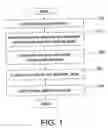
FIG. 1 is a schematic view of the disclosed method;
FIGS. 2A to 2F are schematic cross-sectional views of the manufacturing process according to an embodiment of the invention; and
FIG. 3 is a schematic cross-sectional view of another embodiment of the invention.
DETAILED DESCRIPTIONThe steps of the disclosed method are shown in FIG. 1. First, a molding plate is provided (step 110). Several active components are disposed with alignment on the molding plate (step 120). A dielectric layer is deposited on the molding plate (step 130) to cover the active components. A circuit is made on the dielectric layer (step 140), in contact with the active components. Finally, the molding plate is removed (step 150), releasing the dielectric layer with embedded active components from the molding plate. One then obtains a structure of embedded active components.
When the dielectric layer is a polymer layer, it can be a preprocessed or existing polymer layer, such as the Ajinomoto build-up film (ABF) or the resin coated copper foil (RCC). The above process also includes the step of embossing to embed active components into the polymer layer or the step of coating a polymer solution followed by curing to form the dielectric layer. The latter includes the steps of: covering a polymer solution on the active components by spraying, spin-coating, or printing; and curing the polymer solution to form a polymer layer.
Step 140 in FIG. 1 makes a circuit on the insulator. Several conductive holes connecting to the active components are first formed on the dielectric layer, followed by forming the circuit passing through the conductive holes.
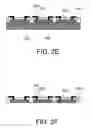
The process in an embodiment of the invention is further described in detail with reference to FIGS. 2A to 2F.
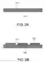
As shown in FIG. 2A, a metal mold-departing layer 210 is deposited on a molding plate 200. The molding material can be Teflon that can be readily removed from the molding plate. The mold-departing layer can be made of any other material with a similar property.
As shown in FIG. 2B, the active components 220 are disposed with alignment on the molding plate 200.
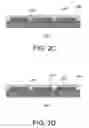
As shown in FIG. 2C, a polymer layer 300 is coated on the molding plate 200 as a dielectric layer to cover the active components. The polymer layer is cured according to the properties of the selected polymer.
As shown in FIG. 2D, several conductive holes 310 connecting to the active components 220 are formed on the polymer layer 300. The conductive holes 310 can be formed using laser, etching, or direct exposure. The conductive holes 310 are further processed by desmearing.
As shown in FIG. 2E, a metal layer 230 is deposited on the polymer layer 300.
Photolithography is employed to transfer the required pattern onto the metal layer 230, forming the circuit with the conductive holes thereon.
Finally, as shown in FIG. 2F, the molding plate is released from the polymer layer 300 embedded with active components 220 to form a structure of embedded active components.
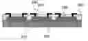
The structure of embedded active components formed using the process of the disclosed embodiment is shown in FIG. 2F to contain the polymer layer 300, the active components 220, and the circuit. The active components 220 are embedded in the polymer layer 300. The circuit is formed on the polymer layer 300 and connected to the active components 220 via the conductive holes.
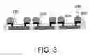
FIG. 3 shows a cross-sectional view of another embodiment of the invention. The above-mentioned structure of embedded active components can be implanted with soldering balls 240 at the contact points of the circuit for subsequent electrical connections.
The disclosed structure of embedded active components can be installed with an arbitrary substrate, such as the semiconductor substrate, flexible substrate, or glass substrate. Since the active components have fixed relative positions, only one alignment is required to fix the positions of all the active components. This can greatly lower the difficulty in subsequent processes and increase the product yield.
Certain variations would be apparent to those skilled in the art, which variations are considered within the spirit and scope of the claimed invention.
Claims
What is claimed is:1. A method of making a structure of embedded active components, comprising the steps of:
providing a molding plate;
disposing with alignment a plurality of active components on the molding plate;
covering a dielectric layer on the molding plate to cap the active components;
forming an electrical circuit on the dielectric layer to be in electrical communications with the active components; and
releasing the dielectric layer embedded with the active components from the molding plate.
2. The method of claim 1, wherein the dielectric layer is a polymer layer.
3. The method of claim 2, wherein the polymer layer is selected from the group consisting of Ajinomoto build-up film (ABF) and resin coated copper foil (RCC).
4. The method of claim 2 further comprising the step of embedding the active components into the polymer layer by embossing.
5. The method of claim 2, wherein the step of covering a dielectric layer on the molding plate contains the steps of:
covering a polymer solution on the active components; and
curing the polymer solution.
6. The method of claim 5, wherein the step of covering a polymer solution on the active components is implemented using a method selected from spraying, spin-coating, and printing.
7. The method of claim 1, wherein the step of forming an electrical circuit on the dielectric layer includes:
forming a plurality of conductive holes connecting to the active components on the dielectric layer; and
forming an electrical circuit passing through the conductive holes.
8. The method of claim 7, wherein the conductive holes are formed by a method selected from laser drilling, exposure and developing, and etching.
9. The method of claim 7, wherein the step of forming an electrical circuit passing through the conductive holes includes the steps of:
depositing a metal layer on the dielectric layer; and
employing photolithography to transfer a required pattern to the metal layer to form the electrical circuit.
10. The method of claim 7 further comprising the step of desmearing the conductive holes.
11. The method of claim 1, wherein the material of the molding plate if Teflon.
12. The method of claim 1, wherein the molding plate contains a mold-separating layer.
13. The method of claim 12, wherein the mold-separating layer is a metal mold-separating layer.
14. The method of claim 1 further comprising the step of implanting soldering balls at contact points of the electrical circuit.
15. A structure of embedded active components, comprising:
a dielectric layer;
a plurality of active components embedded in the dielectric layer; and
an electrical circuit installed on the dielectric layer and in electrical communications with the active components.
16. The structure of embedded active components as in claim 13, wherein the dielectric layer is a polymer layer.
17. The structure of embedded active components as in claim 13, wherein the dielectric layer has a plurality of conductive holes for the electrical circuit to connect to the active components.
18. The structure of embedded active components as in claim 13 further comprising a plurality of soldering balls installed at contact points of the electrical circuit.
Images & Drawings included:
Sources:
- United States Patent and Trademark Office - verify current appl. status at the USPTO↗
Similar patent applications:
Recent applications in this class:
- » 20250149347 2025-05-08
METHOD FOR FABRICATING SEMICONDUCTOR PACKAGING STRUCTURE AND SEMICONDUCTOR PACKAGING STRUCTURE FABRICATED USING THE SAME - » 20250118574 2025-04-10
METHOD OF MANUFACTURING SEMICONDUCTOR PACKAGES - » 20250054776 2025-02-13
SEMICONDUCTOR PACKAGES WITH PATTERNS OF DIE-SPECIFIC INFORMATION - » 20250046624 2025-02-06
METHOD OF PROCESSING WAFER - » 20250006511 2025-01-02
SEMICONDUCTOR DEVICE PACKAGING WARPAGE CONTROL - » 20250006510 2025-01-02
SEMICONDUCTOR DEVICE PACKAGE WITH WETTABLE FLANKS - » 20240395566 2024-11-28
SEMICONDUCTOR DEVICE - » 20240387197 2024-11-21
MANUFACTURING METHOD OF SEMICONDUCTOR PACKAGE - » 20240387196 2024-11-21
Semiconductor Package and Method of Manufacturing The Same - » 20240379383 2024-11-14
SEMICONDUCTOR DEVICE AND METHOD FOR MANUFACTURING THE SAME