Integrated circuit edge protection method and apparatus
US20060223239A1
2006-10-05
11/096,427
2005-03-31
✅ Patent granted
US 7,372,134 B2
2008-05-13
-
-
Roy Potter
2026-03-04
Abstract:
An apparatus, method, and system for providing a mechanical divider adapted to shield at least a portion of an active surface of an integrated circuit from out-gassing from underfill material. The mechanical divider is attached to a mounting substrate. The underfill material is dispensed on the mounting substrate. The integrated circuit is placed on both the mechanical divider and on the underfill material after the mechanical divider has been at least partially cured. The mechanical divider may include a base surface adapted to contact the mounting substrate, a lower wall surface extending upwardly from the base surface, an upper wall surface adapted to abut a side wall of the integrated circuit, and a ledge surface extending between the lower wall surface and the upper wall surface, the ledge surface adapted to contact at least a portion of the active surface of the integrated circuit.
Inventors:
- Zhiyong Wang 15 🇺🇸 Chandler, AZ, United States
- Lee Peng Khaw 2 🇺🇸 Chandler, AZ, United States
- Kam Meng Chong 2 🇲🇾 Penang, Malaysia
- Diego Diaz 2 🇺🇸 Chandler, AZ, United States
- Zezhong Fu 2 🇺🇸 Chandler, AZ, United States
- Kam Meng Chong 1 🇲🇾 Bayan Lepas, Malaysia
Assignee:
- INTEL CORPORATION 47,158 🇺🇸 Santa Clara, CA, United States
Interested in similar patents?
Get notified when new applications in this technology area are published.
Classification:
H01L2924/00012 » CPC further
Indexing scheme for arrangements or methods for connecting or disconnecting semiconductor or solid-state bodies as covered by; Technical content checked by a classifier Relevant to the scope of the group, the symbol of which is combined with the symbol of this group
H01L2224/83192 » CPC further
Indexing scheme for arrangements for connecting or disconnecting semiconductor or solid-state bodies and methods related thereto as covered by; Methods for connecting semiconductor or other solid state bodies using means for bonding being attached to, or being formed on, the surface to be connected using a layer connector; Arrangement of the layer connectors prior to mounting wherein the layer connectors are disposed only on another item or body to be connected to the semiconductor or solid-state body
H01L2224/73204 » CPC further
Indexing scheme for arrangements for connecting or disconnecting semiconductor or solid-state bodies and methods related thereto as covered by; Means for bonding being of different types provided for in two or more of groups; Location after the connecting process on the same surface; Bump and layer connectors the bump connector being embedded into the layer connector
H01L2924/00 » CPC further
Indexing scheme for arrangements or methods for connecting or disconnecting semiconductor or solid-state bodies as covered by
H01L2924/00014 » CPC further
Indexing scheme for arrangements or methods for connecting or disconnecting semiconductor or solid-state bodies as covered by; Technical content checked by a classifier the subject-matter covered by the group, the symbol of which is combined with the symbol of this group, being disclosed without further technical details
H01L2924/00011 » CPC further
Indexing scheme for arrangements or methods for connecting or disconnecting semiconductor or solid-state bodies as covered by; Technical content checked by a classifier Not relevant to the scope of the group, the symbol of which is combined with the symbol of this group
H01L2224/0401 » CPC further
Indexing scheme for arrangements for connecting or disconnecting semiconductor or solid-state bodies and methods related thereto as covered by; Means for bonding being attached to, or being formed on, the surface to be connected, e.g. chip-to-package, die-attach, "first-level" interconnects; Manufacturing methods related thereto; Bonding areas; Manufacturing methods related thereto; Structure, shape, material or disposition of the bonding areas prior to the connecting process Bonding areas specifically adapted for bump connectors, e.g. under bump metallisation [UBM]
H01L21/00 IPC
Processes or apparatus adapted for the manufacture or treatment of semiconductor or solid state devices or of parts thereof
H01L21/563 » CPC main
Processes or apparatus adapted for the manufacture or treatment of semiconductor or solid state devices or of parts thereof; Manufacture or treatment of semiconductor devices or of parts thereof the devices having at least one potential-jump barrier or surface barrier, e.g. PN junction, depletion layer or carrier concentration layer; Assembly of semiconductor devices using processes or apparatus not provided for in a single one of the subgroups - , e.g. sealing of a cap to a base of a container; Encapsulations, e.g. encapsulation layers, coatings Encapsulation of active face of flip-chip device, e.g. underfilling or underencapsulation of flip-chip, encapsulation preform on chip or mounting substrate
H01L24/29 » CPC further
Arrangements for connecting or disconnecting semiconductor or solid-state bodies; Methods or apparatus related thereto; Means for bonding being attached to, or being formed on, the surface to be connected, e.g. chip-to-package, die-attach, "first-level" interconnects; Manufacturing methods related thereto; Layer connectors, e.g. plate connectors, solder or adhesive layers; Manufacturing methods related thereto; Structure, shape, material or disposition of the layer connectors prior to the connecting process of an individual layer connector
H01L24/32 » CPC further
Arrangements for connecting or disconnecting semiconductor or solid-state bodies; Methods or apparatus related thereto; Means for bonding being attached to, or being formed on, the surface to be connected, e.g. chip-to-package, die-attach, "first-level" interconnects; Manufacturing methods related thereto; Layer connectors, e.g. plate connectors, solder or adhesive layers; Manufacturing methods related thereto; Structure, shape, material or disposition of the layer connectors after the connecting process of an individual layer connector
H01L24/83 » CPC further
Arrangements for connecting or disconnecting semiconductor or solid-state bodies; Methods or apparatus related thereto; Methods for connecting semiconductor or other solid state bodies using means for bonding being attached to, or being formed on, the surface to be connected using a layer connector
H01L2224/10165 » CPC further
Indexing scheme for arrangements for connecting or disconnecting semiconductor or solid-state bodies and methods related thereto as covered by; Means for bonding being attached to, or being formed on, the surface to be connected, e.g. chip-to-package, die-attach, "first-level" interconnects; Manufacturing methods related thereto; Bump connectors; Manufacturing methods related thereto; Auxiliary members for bump connectors, e.g. spacers being formed on an item to be connected not being a semiconductor or solid-state body Alignment aids
H01L2224/27013 » CPC further
Indexing scheme for arrangements for connecting or disconnecting semiconductor or solid-state bodies and methods related thereto as covered by; Means for bonding being attached to, or being formed on, the surface to be connected, e.g. chip-to-package, die-attach, "first-level" interconnects; Manufacturing methods related thereto; Layer connectors, e.g. plate connectors, solder or adhesive layers; Manufacturing methods related thereto; Manufacturing methods; Involving a permanent auxiliary member, i.e. a member which is left at least partly in the finished device, e.g. coating, dummy feature for holding or confining the layer connector, e.g. solder flow barrier
H01L2224/73203 » CPC further
Indexing scheme for arrangements for connecting or disconnecting semiconductor or solid-state bodies and methods related thereto as covered by; Means for bonding being of different types provided for in two or more of groups; Location after the connecting process on the same surface Bump and layer connectors
H01L2224/8114 » CPC further
Indexing scheme for arrangements for connecting or disconnecting semiconductor or solid-state bodies and methods related thereto as covered by; Methods for connecting semiconductor or other solid state bodies using means for bonding being attached to, or being formed on, the surface to be connected using a bump connector; Aligning involving guiding structures, e.g. spacers or supporting members the guiding structures being at least partially left in the finished device Guiding structures outside the body
H01L2224/83051 » CPC further
Indexing scheme for arrangements for connecting or disconnecting semiconductor or solid-state bodies and methods related thereto as covered by; Methods for connecting semiconductor or other solid state bodies using means for bonding being attached to, or being formed on, the surface to be connected using a layer connector; Pre-treatment of the layer connector or the bonding area Forming additional members, e.g. dam structures
H01L2924/01033 » CPC further
Indexing scheme for arrangements or methods for connecting or disconnecting semiconductor or solid-state bodies as covered by; Chemical elements Arsenic [As]
H01L2924/14 » CPC further
Indexing scheme for arrangements or methods for connecting or disconnecting semiconductor or solid-state bodies as covered by; Details of semiconductor or other solid state devices to be connected; Device type Integrated circuits
H01L2924/3025 » CPC further
Indexing scheme for arrangements or methods for connecting or disconnecting semiconductor or solid-state bodies as covered by; Technical effects; Electrical effects Electromagnetic shielding
H01L23/02 IPC
Details of semiconductor or other solid state devices Containers; Seals
Description
FIELD OF THE INVENTIONDisclosed embodiments of the present invention relate to the field of integrated circuits, and more particularly to integrated circuit packaging.
BACKGROUND OF THE INVENTIONWith the advancement of integrated circuit technology, the need to miniaturize integrated circuit packaging to meet the needs of this integrated circuit technology has increased exponentially. This requirement has resulted in chip-scale packaging, wherein the ultimate goal is to have both the integrated circuit and the integrated circuit package be virtually the same size.
An integrated circuit package usually includes a mounting substrate and an integrated circuit, such as a semiconductor chip or die. The integrated circuit is located on or in the mounting substrate. One class of chip packaging includes integrated circuits that are produced with solder contacts, on an active surface thereof, for purposes of electrically connecting the integrated circuit to solder deposits on the mounting substrate. The term active surface of an integrated circuit, as used herein, means the surface which carries integrated circuitry. The term back surface, as used herein, means a side of the integrated circuit that is positioned opposite and parallel planar with the active surface.
During packaging, an epoxy underfill material is introduced into a space between the integrated circuit and the mounting substrate and is cured thereafter. The epoxy acts to bond the integrated circuit to the mounting substrate and to protect the solder contacts. The underfill material that has been inserted between the integrated circuit and the mounting substrate typically has a non-uniform profile. The non-uniform profile is often due to the underfill material including both an interstitial portion that is sandwiched between the integrated circuit and the mounting substrate, as well as a fillet portion that extends diagonally from the integrated circuit side walls to the mounting substrate.
BRIEF DESCRIPTION OF THE DRAWINGSEmbodiments of the invention are illustrated by way of example and not by way of limitation in the figures of the accompanying drawings, in which the like references indicate similar elements and in which:
FIG. 1 is a perspective view illustrating an electronic assembly, in accordance with some embodiments of the present invention;
FIG. 2 is a cross sectional view taken along line 2--2 in FIG. 1 illustrating an example electronic assembly, in accordance with an embodiment of the present invention;
FIGS. 3, 4, 5, 6, and 6A are cross sectional views taken along line 2--2 in FIG. 1 illustrating the example electronic assembly of FIG. 2 at various stages of construction, in accordance with an embodiment of the present invention;
FIG. 7 is a cross sectional view taken along line 2--2 in FIG. 1 illustrating an attachment of a mechanical divider in the example electronic assembly of FIG. 2, in accordance with an embodiment of the present invention;
FIG. 8 is a cross sectional view taken along line 2--2 in FIG. 1 illustrating an attachment of a mechanical divider in the example electronic assembly of FIG. 2, in accordance with an embodiment of the present invention; and
FIG. 9 is a system including an electronic assembly in accordance with an embodiment of the present invention.
DETAILED DESCRIPTION OF EMBODIMENTS OF THE INVENTIONAn apparatus, method, and system for providing a mechanical divider adapted to shield at least a portion of an active surface of an integrated circuit from out-gassing from underfill material in an electronic assembly is disclosed herein. In the following detailed description, reference is made to the accompanying drawings which form a part hereof wherein like numerals designate like parts throughout, and in which is shown by way of illustration specific embodiments in which the invention may be practiced. It is to be understood that other embodiments may be utilized and structural or logical changes may be made without departing from the scope of the embodiments of the present invention. It should also be noted that directions and references (e.g., up, down, top, bottom, etc.) may be used to facilitate the discussion of the drawings and are not intended to restrict the application of the embodiments of this invention. Therefore, the following detailed description is not to be taken in a limiting sense and the scope of the embodiments of the present invention is defined by the appended claims and their equivalents.
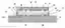
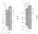
FIG. 1 illustrates a portion of an electronic assembly 10, in accordance with one embodiment. The electronic assembly 10 may be a semiconductor package. The semiconductor package 10 may include an integrated circuit 16 secured to a mounting substrate 14. The integrated circuit 16 may be formed in a rectangular piece of semiconductor material called a chip or a die. Examples of the semiconductor material include, but are not limited to silicon, silicon on sapphire, and gallium arsenide. In some embodiments of the present invention, the integrated circuit 16 may be a processor. For example the integrated circuit 16 may be a microprocessor.
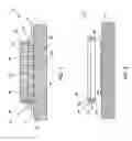
FIG. 2 illustrates an example electronic assembly 10, in accordance with an embodiment of the present invention. In some embodiments of the present invention, a mechanical divider 18 may be located between integrated circuit 16 and substrate 14. The mechanical divider 18 may contact both the integrated circuit 16 and substrate 14. The mechanical divider 18 may be adapted to shield at least a portion of an active surface 20 of the integrated circuit 16 from out-gassing from underfill material. The mechanical divider 18 may be formed of any suitable material, according to the requirements of the particular application. Examples of materials suitable for forming the mechanical divider 18 include, but are not limited to underfill materials such as epoxy and the like.
The mechanical insert 18 may include a base surface 22 adapted to contact the mounting substrate 14. A lower wall surface 24 may extend upwardly from the base surface 22. The lower wall surface 24 may be positioned to surround a first layer of underfill material 26 as well as a solder joint 28 connecting the integrated circuit 16 to the mounting substrate 14. The first layer of underfill material 26 may be formed of any suitable material, according to the requirements of the particular application. Examples of materials suitable for forming the first layer of underfill material 26 include, but are not limited to epoxy and the like. Additionally or alternatively, the underfill material 26 may be formed as no flow underfill. Further, the mechanical divider 18 may be formed of the same or different material from the first layer of underfill material 26.
An upper wall surface 30 may be located above the lower wall surface 24. The upper wall surface 30 may be horizontally displaced relative to the lower wall surface 24 so as to lie in a plane separate from a plane of the lower wall surface 24. The upper wall surface 30 may be adapted to abut a side wall 32 of the integrated circuit 16. The upper wall surface 30 may be adapted to minimize movement of the side wall 32 of the integrated circuit 16 with respect to the mounting substrate 14. Additionally or alternatively, the upper wall surface 30 may be adapted to align the side wall 32 of the integrated circuit 16 with respect to the mounting substrate 14.
A ledge surface 34 may extend between the lower wall surface 24 and the upper wall surface 30. The ledge surface 34 may be adapted to contact at least a portion of the active surface 20 of the integrated circuit 16. The ledge surface 34 may be adapted to fix the distance between the active surface 20 of the integrated circuit 16 and the mounting substrate 14. Further, the ledge surface 34 may be adapted to minimize movement of active surface 20 of the integrated circuit 16 with respect to the mounting substrate 14.
Additionally or alternatively, the ledge surface 34 may be adapted to shield at least a portion of the active surface 20 of the integrated circuit 16 from out-gassing from the first layer of underfill material 26. For example, the ledge surface 34 may contact and shield an edge portion 36 of the active surface 20 of the integrated circuit 16 from the first layer of underfill material 26, while leaving an inner portion 38 of the active surface 20 of the integrated circuit 16 open to the first layer of underfill material 26. The chemical reaction during polymerization of the first layer of underfill material 26 may result in out-gassing. This out-gassing may facilitate the formation of voids within the first layer of underfill material 26. In addition, these voids may be transported to an outer portion of the first layer of underfill material 26 near the edge portion 36 of the active surface 20 of the integrated circuit 16 as pressure build-up occurs at the inner portion 38 of the active surface 20 of the integrated circuit 16. The ledge surface 34 may shield the edge portion 36 of the active surface 20 of the integrated circuit 16 from the voids in the first layer of underfill material 26. Additionally or alternatively, the transportation of the voids from the first layer of underfill material 26 may be limited by locating the lower wall surface 24 adjacent the inner portion 38 of the active surface 20 of the integrated circuit 16.
An outer wall surface 40 of the mechanical insert 18 may be positioned opposite the lower wall surface 24. The outer wall surface 40 may extend upwardly from the base surface 22. The outer wall surface 40 may be positioned to be surrounded by a second layer of underfill material 42 connecting the integrated circuit 16 to the mounting substrate 14. Accordingly, the mechanical insert 18 may be positioned between the first layer of underfill material 26 and the second layer of underfill material 42. The second layer of underfill material 42 may be formed of any suitable material, according to the requirements of the particular application. Examples of materials suitable for forming the second layer of underfill material 42 include, but are not limited to epoxy and the like. Additionally or alternatively, the underfill material 42 may be formed as no flow underfill. Further, the second layer of underfill material 42 may be formed of the same or different material from the first layer of underfill material 26.
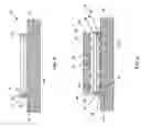
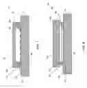
FIGS. 3, 4, 5, 6, and 6A illustrate an example electronic assembly 10 at given stages of construction, in accordance with an embodiment of the present invention. A solder contact 44 may be formed on an upper surface of the mounting substrate 14 to face the integrated circuit 16. Similarly, solder deposit 46 may be formed on the bottom surface of the integrated circuit 16 to face the mounting substrate 14. The solder contact 44 and/or the solder deposit 46 may be formed as a solder ball or other suitable shape, according to the requirements of the particular application. For example, the solder deposit 46 may be formed as a dimple-less bump having a concave shape. The lower wall surface 24 of the mechanical divider 18 may be adapted to form an opening to receive the solder deposit 46 on the integrated circuit 16 as well as to receive the solder contact 44 of the mounting substrate 14.
FIG. 4 illustrates an example electronic assembly 10 at a given stage of construction, in accordance with an embodiment of the present invention. The mechanical insert 18 may be attached to the mounting substrate 14 by any suitable method. For example, FIG. 7 illustrates an example electronic assembly 10 at a given stage of construction, in accordance with an embodiment of the present invention, where a mold 48 dispenses an at least partially cures the mechanical insert 18 to the mounting substrate 14. After the mechanical insert 18 is dispensed and an at least partially cured, the mold 48 may be removed. Alternatively, FIG. 8 illustrates an example electronic assembly 10 at a given stage of construction, in accordance with an embodiment of the present invention, where a placement tool 50 places a pre-formed and at least partially cured the mechanical insert 18 on the mounting substrate 14. After the mechanical insert 18 is placed on the mounting substrate, the placement tool 50 may be removed. According to the requirements of the particular application, the mechanical divider 18 may be at least partially cured prior to the placing of the integrated circuit 16 on the first layer of underfill material 26; the mechanical divider 18 may be at least partially cured while attached to the mounting substrate 14; and/or the mechanical divider 18 may be at least partially cured prior to attaching to the mounting substrate 14.
FIG. 5 illustrates an example electronic assembly 10 at a given stage of construction, in accordance with an embodiment of the present invention. The first layer of underfill material 26 may be dispensed onto the mounting substrate 14. The first layer of underfill material 26 may be dispensed within the lower wall surface 24 of the mechanical divider 18 and below the ledge surface 34 of the mechanical divider 18.
FIG. 6 illustrates an example electronic assembly 10 at a given stage of construction, in accordance with an embodiment of the present invention. At least a portion of the active surface 20 of the integrated circuit 16 may be placed on the first layer of underfill material 26. For example, the inner portion 38 of the active surface 20 of the integrated circuit 16 may be placed on the first layer of underfill material 26. At least a portion of the active surface 20 of the integrated circuit 16 may be placed on the ledge surface 34 of the mechanical divider 18. For example, the edge portion 36 of the active surface 20 of the integrated circuit 16 may be placed on the first layer of underfill material 26.
FIG. 6A illustrates an example electronic assembly 10 at a given stage of construction, in accordance with an embodiment of the present invention. Once integrated circuit 16 is placed on the mechanical insert 18 and the mounting substrate 14, the second layer of underfill material 42 may be dispensed on the mounting substrate 14. The second layer of underfill material 42 may contact one or both of the mechanical divider 18 and a non-active surface of the integrated circuit 16, such as the side wall 32.
With reference back to FIG. 2, Once the second layer of underfill material 42 is dispensed on the mounting substrate 14, reflow of the solder deposit 46 (FIG. 6A) and the solder contact 44 (FIG. 6A) may be performed. The reflow of the solder deposit 46 (FIG. 5) and the solder contact 44 (FIG. 6A) creates the solder joint 28 connecting the integrated circuit 16 to the mounting substrate 14. For example, thermal compression bonding may be used to reflow of the solder deposit 46 (FIG. 6A) and the solder contact 44 (FIG. 6A).
FIG. 9 illustrates a block diagram of one of many possible electronic systems 60 in which embodiments of the present invention may be used. The electronic system 60 may utilize one or more embodiments of the electronic assembly 10 described herein. As shown, the system 60 includes a processor 62, such as an integrated circuit, and temporary memory 64, such as SDRAM and DRAM, on high-speed bus 66. Voltage regulator 68 may be utilized to provide power to processor 62 via traces 70. The high-speed bus 66 is connected through bus bridge 72 to input/output (I/O) bus 74. I/O bus 74 connects permanent memory 76, such as flash devices and mass storage device (e.g. fixed disk device), and I/O devices 78 to each other and bus bridge 72. In various embodiments, system 60 may be a set-top box, a digital camera, a CD player, a DVD player, a wireless mobile phone, a tablet computing device, or a laptop computing device.
Although specific embodiments have been illustrated and described herein for purposes of description of the preferred embodiment, it will be appreciated by those of ordinary skill in the art that a wide variety of alternate and/or equivalent implementations calculated to achieve the same purposes may be substituted for the specific embodiment shown and described without departing from the scope of the present invention. Those with skill in the art will readily appreciate that the present invention may be implemented in a very wide variety of embodiments. This application is intended to cover any adaptations or variations of the embodiments discussed herein. Therefore, it is manifestly intended that this invention be limited only by the claims and the equivalents thereof.
Claims
What is claimed is:1. A method, comprising:
dispensing a first layer of underfill material on a mounting substrate;
placing at least a portion of an active surface of an integrated circuit on the first layer of underfill material; and
shielding at least a portion of the active surface of the integrated circuit from out-gassing from the first layer of underfill material.
2. The method of claim 1, further comprising shielding at least a portion of the active surface of the integrated circuit from out-gassing from the first layer of underfill material with a mechanical divider attached to the mounting substrate.
3. The method of claim 2, further comprising at least partially curing the mechanical divider prior to the placing of the integrated circuit on the first layer of underfill material.
4. The method of claim 3, wherein the mechanical divider is at least partially cured while attached to the mounting substrate.
5. The method of claim 3, wherein the mechanical divider is at least partially cured prior to attaching to the mounting substrate.
6. The method of claim 2, further comprising dispensing a second layer of underfill material on the mounting substrate, the second layer of underfill material contacting both a non-active surface of the integrated circuit and the mechanical divider.
7. An apparatus comprising:
a base surface adapted to contact a mounting substrate;
a lower wall surface extending upwardly from the base surface;
an upper wall surface adapted to abut a side wall of an integrated circuit; and
a ledge surface extending between the lower wall surface and the upper wall surface, the ledge surface adapted to contact at least a portion of an active surface of an integrated circuit.
8. The apparatus of claim 7, wherein the ledge surface is adapted to shield at least a portion of an active surface of an integrated circuit from out-gassing from no flow underfill.
9. The apparatus of claim 7, wherein the ledge surface is adapted to fix the distance between an active surface of an integrated circuit and a mounting substrate.
10. The apparatus of claim 7, wherein the ledge surface is adapted to minimize movement of an active surface of an integrated circuit with respect to a mounting substrate.
11. The apparatus of claim 7, wherein the upper wall surface is adapted to align a side wall of an integrated circuit with respect to a mounting substrate.
12. The apparatus of claim 7, wherein the upper wall surface is adapted to minimize movement of a side wall of an integrated circuit with respect to a mounting substrate.
13. A method, comprising:
attaching a mechanical divider to a mounting substrate;
dispensing a first layer of underfill material on the mounting substrate; and
placing an integrated circuit on both the mechanical divider and on the first layer of underfill material after the mechanical divider has been at least partially cured.
14. The method of claim 13, further comprising dispensing a second layer of underfill material on the mounting substrate, the second layer of underfill material contacting both a non-active surface of the integrated circuit and the mechanical divider.
15. The method of claim 13, wherein the mechanical divider is at least partially cured while attached to the mounting substrate.
16. The method of claim 13, wherein the mechanical divider is at least partially cured prior to attaching to the mounting substrate.
17. The method of claim 13, further comprising the mechanical divider fixing the distance between an active surface of the integrated circuit and the mounting substrate.
18. The method of claim 13, further comprising the mechanical divider minimizing movement of an active surface of the integrated circuit with respect to the mounting substrate.
19. The method of claim 13, further comprising the mechanical divider aligning a side wall of the integrated circuit with respect to the mounting substrate.
20. The method of claim 13, further comprising the mechanical divider minimizing movement of a side wall of the integrated circuit with respect to the mounting substrate.
21. A system comprising:
a semiconductor package having an integrated circuit coupled to a mounting substrate;
a mechanical divider comprising:
a base surface adapted to contact the mounting substrate,
a lower wall surface extending upwardly from the base surface,
an upper wall surface adapted to abut a side wall of the integrated circuit, and
a ledge surface extending between the lower wall surface and the upper wall surface, the ledge surface adapted to contact at least a portion of an active surface of the integrated circuit;
a bus coupled to the semiconductor package; and
a mass storage coupled to the bus.
22. The system of claim 21, wherein the system is selected from the group consisting of a set-top box, a digital camera, a CD player, a DVD player, a wireless mobile phone, a tablet computing device, and a laptop computing device.
23. The system of claim 21, wherein the ledge surface is adapted to shield at least a portion of the active surface of the integrated circuit from out-gassing from no flow underfill.
24. The system of claim 21, wherein the ledge surface is adapted to fix the distance between the active surface of the integrated circuit and the mounting substrate; the ledge surface is adapted to minimize movement of the active surface of the integrated circuit with respect to the mounting substrate; the upper wall surface is adapted to align a side wall of the integrated circuit with respect to the mounting substrate; and the upper wall surface is adapted to minimize movement of a side wall of the integrated circuit with respect to the mounting substrate.
Images & Drawings included:
Sources:
- United States Patent and Trademark Office - verify current appl. status at the USPTO↗
Similar patent applications:
Recent applications in this class:
- » 20250293051 2025-09-18
PACKAGE STRUCTURE WITH UNDERFILL - » 20250266266 2025-08-21
MOLDED PACKAGES IN A MOLDED DEVICE - » 20250246445 2025-07-31
FLIP CHIP PACKAGE UNIT AND ASSOCIATED PACKAGING METHOD - » 20250157828 2025-05-15
SEMICONDUCTOR ASSEMBLIES WITH UNDERFILL SQUEEZE-UP, AND METHODS FOR MAKING THE SAME - » 20250118575 2025-04-10
INTEGRATED CIRCUIT PACKAGE AND METHOD OF FORMING THEREOF - » 20250096009 2025-03-20
LOW COST PACKAGE WARPAGE SOLUTION - » 20240395567 2024-11-28
SELECTIVE UNDERFILLING USING PRE-APPLIED THERMOSET ADHESIVE - » 20240387198 2024-11-21
Integrated Circuit Package and Method - » 20240339336 2024-10-10
SUBSTRATE HAVING UNDERFILL DAM AND SEMICONDUCTOR PACKAGE INCLUDING THE SAME, AND METHOD FOR MANUFACTURING THE SEMICONDUCTOR PACKAGE - » 20240312798 2024-09-19
SEMICONDUCTOR DIE PACKAGE WITH RING STRUCTURE
Recent applications for this Assignee:
- » 20250294866 2025-09-18
GATE CUT CONFINED WITHIN GATE TRENCH - » 20250294846 2025-09-18
BACKSIDE CROSS-COUPLE INTERCONNECTS - » 20250294835 2025-09-18
ELONGATED VERTICAL STRUCTURES OF CHANNEL MATERIALS - » 20250294827 2025-09-18
CO-INTEGRATION OF GATE-ALL-AROUND DEVICES WITH DIFFERENT NUMBERS OF NANORIBBONS - » 20250294818 2025-09-18
TRANSISTOR DESIGNS FOR FLOATING BODY MEMORY - » 20250294781 2025-09-18
MAGNETIC CORE INDUCTORS ON PACKAGE SUBSTRATES - » 20250294777 2025-09-18
INTEGRATED CIRCUIT DEVICE WITH MEMORY ARRAY AND SHARED GAIN ELEMENT - » 20250293985 2025-09-18
RECEIVER-BASED PRECISION CONGESTION CONTROL - » 20250293860 2025-09-18
PRESERVATION OF CONFIDENTIALITY AND INTEGRITY OF MODELS DURING EXECUTION - » 20250293706 2025-09-18
LOW-RANK DECOMPOSITION-BASED HARDWARE COMPRESSION OF MATRICES AND TENSORS