Pillar grid array package
US20060231941A1
2006-10-19
11/228,234
2005-09-19
✅ Patent granted
US 7,368,809 B2
2008-05-06
-
-
Hsien-Ming Lee
2026-02-09
Abstract:
A pillar grid array package (PGA) includes a substrate, a chip disposed on top of the substrate, and a plurality of stud bumps disposed on bottom of the substrate. The stud bumps are formed in an array and each has a flattened top to electrically connect to a printed circuit board, PCB, by an anisotropic conductive paste to achieve a thin package and to avoid substrate warpage problems of a ball grid array (BGA) during high-temperature reflow processes.
Inventors:
- Hsiang-Ming Huang 12 🇹🇼 Tainan, Taiwan
- An-Hong Liu 26 🇹🇼 Tainan, Taiwan
- Yi-Chang Lee 14 🇹🇼 Tainan, Taiwan
- Yeong-Ching Chao 13 🇹🇼 Tainan, Taiwan
Assignee:
- CHIPMOS TECHNOLOGIES INC. 196 🇹🇼 Hsinchu, Taiwan
- ChipMOS Technologies (Bermuda) Ltd. 1 Hamilton HM 12, Bermuda
Interested in similar patents?
Get notified when new applications in this technology area are published.
Classification:
H01L21/4853 » CPC main
Processes or apparatus adapted for the manufacture or treatment of semiconductor or solid state devices or of parts thereof; Manufacture or treatment of semiconductor devices or of parts thereof the devices having at least one potential-jump barrier or surface barrier, e.g. PN junction, depletion layer or carrier concentration layer; Manufacture or treatment of parts, e.g. containers, prior to assembly of the devices, using processes not provided for in a single one of the subgroups -; Conductive parts; Leads on or in insulating or insulated substrates, e.g. metallisation Connection or disconnection of other leads to or from a metallisation, e.g. pins, wires, bumps
H01L23/13 » CPC further
Details of semiconductor or other solid state devices; Mountings, e.g. non-detachable insulating substrates characterised by the shape
H01L23/3114 » CPC further
Details of semiconductor or other solid state devices; Encapsulations, e.g. encapsulating layers, coatings, e.g. for protection characterised by the arrangement or shape the device being completely enclosed the device being a chip scale package, e.g. CSP
H01L23/3128 » CPC further
Details of semiconductor or other solid state devices; Encapsulations, e.g. encapsulating layers, coatings, e.g. for protection characterised by the arrangement or shape the device being completely enclosed a substrate forming part of the encapsulation the substrate having spherical bumps for external connection
H01L23/49811 » CPC further
Details of semiconductor or other solid state devices; Arrangements for conducting electric current to or from the solid state body in operation, e.g. leads, terminal arrangements ; Selection of materials therefor consisting of soldered constructions; Leads, on insulating substrates, Additional leads joined to the metallisation on the insulating substrate, e.g. pins, bumps, wires, flat leads
H01L21/563 » CPC further
Processes or apparatus adapted for the manufacture or treatment of semiconductor or solid state devices or of parts thereof; Manufacture or treatment of semiconductor devices or of parts thereof the devices having at least one potential-jump barrier or surface barrier, e.g. PN junction, depletion layer or carrier concentration layer; Assembly of semiconductor devices using processes or apparatus not provided for in a single one of the subgroups - , e.g. sealing of a cap to a base of a container; Encapsulations, e.g. encapsulation layers, coatings Encapsulation of active face of flip-chip device, e.g. underfilling or underencapsulation of flip-chip, encapsulation preform on chip or mounting substrate
H01L24/45 » CPC further
Arrangements for connecting or disconnecting semiconductor or solid-state bodies; Methods or apparatus related thereto; Means for bonding being attached to, or being formed on, the surface to be connected, e.g. chip-to-package, die-attach, "first-level" interconnects; Manufacturing methods related thereto; Wire connectors; Manufacturing methods related thereto; Structure, shape, material or disposition of the wire connectors prior to the connecting process of an individual wire connector
H01L24/48 » CPC further
Arrangements for connecting or disconnecting semiconductor or solid-state bodies; Methods or apparatus related thereto; Means for bonding being attached to, or being formed on, the surface to be connected, e.g. chip-to-package, die-attach, "first-level" interconnects; Manufacturing methods related thereto; Wire connectors; Manufacturing methods related thereto; Structure, shape, material or disposition of the wire connectors after the connecting process of an individual wire connector
H01L2224/04042 » CPC further
Indexing scheme for arrangements for connecting or disconnecting semiconductor or solid-state bodies and methods related thereto as covered by; Means for bonding being attached to, or being formed on, the surface to be connected, e.g. chip-to-package, die-attach, "first-level" interconnects; Manufacturing methods related thereto; Bonding areas; Manufacturing methods related thereto; Structure, shape, material or disposition of the bonding areas prior to the connecting process Bonding areas specifically adapted for wire connectors, e.g. wirebond pads
H01L2224/73204 » CPC further
Indexing scheme for arrangements for connecting or disconnecting semiconductor or solid-state bodies and methods related thereto as covered by; Means for bonding being of different types provided for in two or more of groups; Location after the connecting process on the same surface; Bump and layer connectors the bump connector being embedded into the layer connector
H01L2224/73215 » CPC further
Indexing scheme for arrangements for connecting or disconnecting semiconductor or solid-state bodies and methods related thereto as covered by; Means for bonding being of different types provided for in two or more of groups; Location after the connecting process on the same surface Layer and wire connectors
H01L2224/92147 » CPC further
Indexing scheme for arrangements for connecting or disconnecting semiconductor or solid-state bodies and methods related thereto as covered by; Methods for connecting semiconductor or solid state bodies including different methods provided for in two or more of groups - ; Specific sequence of method steps; Connecting a surface with connectors of different types; Sequential connecting processes the first connecting process involving a layer connector the second connecting process involving a wire connector
H01L2924/01079 » CPC further
Indexing scheme for arrangements or methods for connecting or disconnecting semiconductor or solid-state bodies as covered by; Chemical elements Gold [Au]
H01L2924/01322 » CPC further
Indexing scheme for arrangements or methods for connecting or disconnecting semiconductor or solid-state bodies as covered by; Alloys; Binary Alloys Eutectic Alloys, i.e. obtained by a liquid transforming into two solid phases
H01L2924/14 » CPC further
Indexing scheme for arrangements or methods for connecting or disconnecting semiconductor or solid-state bodies as covered by; Details of semiconductor or other solid state devices to be connected; Device type Integrated circuits
H01L2924/15311 » CPC further
Indexing scheme for arrangements or methods for connecting or disconnecting semiconductor or solid-state bodies as covered by; Details of package parts other than the semiconductor or other solid state devices to be connected; Die mounting substrate; Connection portion the connection portion being formed only on the surface of the substrate opposite to the die mounting surface being a ball array, e.g. BGA
H01L2924/00 » CPC further
Indexing scheme for arrangements or methods for connecting or disconnecting semiconductor or solid-state bodies as covered by
H01L2224/05599 » CPC further
Indexing scheme for arrangements for connecting or disconnecting semiconductor or solid-state bodies and methods related thereto as covered by; Means for bonding being attached to, or being formed on, the surface to be connected, e.g. chip-to-package, die-attach, "first-level" interconnects; Manufacturing methods related thereto; Bonding areas; Manufacturing methods related thereto; Structure, shape, material or disposition of the bonding areas prior to the connecting process of an individual bonding area; External layer Material
H01L2924/00014 » CPC further
Indexing scheme for arrangements or methods for connecting or disconnecting semiconductor or solid-state bodies as covered by; Technical content checked by a classifier the subject-matter covered by the group, the symbol of which is combined with the symbol of this group, being disclosed without further technical details
H01L2924/00011 » CPC further
Indexing scheme for arrangements or methods for connecting or disconnecting semiconductor or solid-state bodies as covered by; Technical content checked by a classifier Not relevant to the scope of the group, the symbol of which is combined with the symbol of this group
H01L2224/0401 » CPC further
Indexing scheme for arrangements for connecting or disconnecting semiconductor or solid-state bodies and methods related thereto as covered by; Means for bonding being attached to, or being formed on, the surface to be connected, e.g. chip-to-package, die-attach, "first-level" interconnects; Manufacturing methods related thereto; Bonding areas; Manufacturing methods related thereto; Structure, shape, material or disposition of the bonding areas prior to the connecting process Bonding areas specifically adapted for bump connectors, e.g. under bump metallisation [UBM]
H01L23/24 IPC
Details of semiconductor or other solid state devices; Fillings or auxiliary members in containers or encapsulations , e.g. centering rings; Fillings characterised by the material, its physical or chemical properties, or its arrangement within the complete device solid or gel at the normal operating temperature of the device
H01L23/52 IPC
Details of semiconductor or other solid state devices Arrangements for conducting electric current within the device in operation from one component to another, i.e. interconnections, e.g. wires, lead frames
H01L23/02 IPC
Details of semiconductor or other solid state devices Containers; Seals
H01L21/44 IPC
Processes or apparatus adapted for the manufacture or treatment of semiconductor or solid state devices or of parts thereof; Manufacture or treatment of semiconductor devices or of parts thereof the devices having at least one potential-jump barrier or surface barrier, e.g. PN junction, depletion layer or carrier concentration layer the devices having semiconductor bodies not provided for in groups, , , and with or without impurities, e.g. doping materials Manufacture of electrodes on semiconductor bodies using processes or apparatus not provided for in groups -
Description
FIELD OF THE INVENTIONThe present invention relates to an IC package, and more particularly, to an IC package with pillar grid array (PGA) configuration.
BACKGROUND OF THE INVENTIONThe well-known ball grid array package (BGA) is to place solder balls on a substrate in an array for mounting on a printed circuit board (PCB) by surface mount technology, SMT, to achieve the maximum pin counts within the minimum footprint.
As shown in FIG. 1, a conventional BGA package 100 includes a substrate 110, a chip 120 and a plurality of solder balls 140. The chip 120 is disposed on the top surface 111 of the substrate 110 wherein the chip 120 is a bumped chip with a plurality of bumps 122 disposed on the active surface 121 of the chip 120. Then the chip 120 is flipped and electrically connected to the substrate 110 by means of the bumps 122. A plurality of solder balls 140 arranging in an array are disposed on the bottom surface 112 of the substrate 110 to electrically connect to the SMT surface 11 of the PCB 10. Normally, an underfill 130 is disposed between the chip 120 and the substrate 110 to encapsulate the bumps 122.
When the BGA package 100 is attached to the PCB 10 by SMT, in order to electrically connect the solder balls 140 to the connecting pads of the PCB, a high-temperature reflow process is necessary. However, during the reflow process, the substrate 110 can be easily warpaged due to the high reflowing temperature. Normally, the maximum stress is concentrated on parts of the solder balls 140 close to the edges of the substrate 110. The solder balls 140 can be easily broken leading to electrically open. In order to increase the bonding strength of the solder balls 140, larger solder balls are preferred but will easily cause bridging during SMT processes.
SUMMARY OF THE INVENTIONThe main purpose of the present invention is to provide a pillar grid array package (PGA). A plurality of stud bumps formed by wiring-bonding are disposed in an array on the bottom surface of a substrate wherein each stud bump has a flattened top exposed for electrically connecting to the connecting pads of a PCB by anisotropic conductive paste (ACP), anisotropic conductive film (ACF), or ultra-sonic bonding without high-temperature reflow processes to eliminate substrate warpages, moreover, to achieve thinner IC packages.
The second purpose of the present invention is to provide a pillar grid array package wherein a plurality of stud bumps are disposed under a substrate and each has a flattened top with good coplanarity to electrically connect to a PCB. Preferably, these stud bumps have curved sidewalls to reduce lateral bridging.
According to the present invention, a pillar grid array package mainly includes a substrate, a chip and a plurality of stud bumps wherein the substrate has a top surface and a bottom surface. The chip is disposed on the top surface of the substrate. The stud bumps are disposed on the bottom surface of the substrate in an array wherein each stud bump has a flattened top exposed to replace the solder balls of conventional BGA packages to eliminate the conventional high temperature reflow processes.
DESCRIPTION OF THE DRAWINGSFIG. 1 is a cross-sectional view of a conventional BGA package.
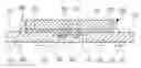
FIG. 2 is a cross-sectional view of a Pillar Grid Array (PGA) package according to the first embodiment of the present invention.
FIG. 3 is the cross-sectional view of the PGA package during wire bonding and stud bond forming processes according to the first embodiment of the present invention.
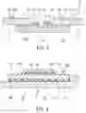
FIG. 4 is another PGA package according to the second embodiment of the present invention.
DETAIL DESCRIPTION OF THE INVENTIONPlease refer to the attached drawings, the present invention will be described by means of embodiment(s) below.
In the first embodiment according to the present invention, as shown in FIG. 2, a PGA (Pillar Grid Array) package 200 mainly includes a substrate 210, a chip 220, and a plurality of stud bumps 250. The substrate 210 has a top surface 211 and a bottom surface 212. In this embodiment, the substrate 210 further has a slot 214 for exposing the bonding pads 222 of the chip 220 and has a plurality of inner bonding fingers 215 around the slot 214. Preferably, the slot 213 has a multi-tier structure where the inner bonding fingers 215 are disposed on the multi-tier structure to reduce the loop height of a plurality of bonding wires 240 to further reduce the thickness of the encapsulant 260. Furthermore, a plurality of outer bonding pads 216 are disposed on the bottom surface 212 of the substrate 210 for bonding the stud bumps 250.
Please refer to FIG. 2 again. The chip 220 is disposed on the top surface 211 of the substrate 210 by a die-attach adhesive material 230 to attach the active surface 221 of the chip 220 to the top surface 211 of the substrate 210. In the embodiment of the present invention, a plurality of bonding pads 222 on the active surface 221 of the chip 220 are exposed from the slot 213 where the bonding pads 222 of the chip 220 are electrically connected to the inner fingers 215 of the substrate 210 by a plurality of bonding wires 240 through the slot 213.
Furthermore, a plurality of stud bumps 250 are disposed in an array on the bottom surface 212 of the substrate 210 where the stud bumps 250 are bonded to the outer bonding pads 216 to be outer electrical connectors of a PGA package to replace the solder balls of a BGA package. The stud bumps 250 are formed by wire bonding which may contain gold, copper, aluminum, or other metals. Moreover, every stud bump 250 has a flattened top 251 exposed which is formed by means of polishing, cutting or etching as pillar bumps to provide a good bonding surface for ACP (anisotropic conductive paste), ACF (anisotropic conductive film) or ultra-sonic eutectic bonding. Preferably, the flattened tops 251 are coplanar to achieve good ACP electrical connection.
Moreover, an encapsulant 160 is formed inside the slot 213 to encapsulate the bonding wires 240, bonding pads 222 and the inner fingers 215. Since the loop height of the bonding wires 240 are lower, therefore, the encapsulant 260 will not protrude from the bottom surface 212 of the substrate 210. In the present embodiment, the encapsulant 260 further encapsulates the sides of the chip 220.
Since the bonding wires 240 and the stud bumps 250 are formed by wire bonding, please refer to FIG. 3, a smaller capillary tool 21 is used to form the bonding wires 240, and a larger capillary tool 22 with gold (Au) wires to form the stud bumps 250 during a same wire bonding process. Then after encapsulating, the substrate 210 is processed by a flattening machine, not shown in the figure, to form the exposed flattened tops 251 of the stud bumps 250 with good coplanarity. The conventional solder ball placement can be eliminated to simplify the overall packaging processes. The stud bumps 250 formed by wire bonding have curved sidewalls 252 which are different from the conventional pillar bumps to reduce the lateral bridging.
Therefore, the PGA 200 can be mounted on a PCB by SMT, not shown in the figure, by ACP or ultra-sonic bonding to form a thin electronic device. The high-temperature reflow processes can be eliminated during SMT processes to eliminate the warpage of the substrate 210 and the breaks of the stud bumps 250.
According to the second embodiment of the present invention, as shown in FIG. 4, a PGA package 300 can be mounted on the SMT surface 11 of a PCB 10 by a ACP 30 (anisotropic conductive paste) or ACF (anisotropic conductive film) to form a thin electronic device. The PGA package 300 includes a substrate 310, a chip 320, and a plurality of stud bumps 340 where the substrate 310 is a rigid or flex PCB having a top surface 311 and a bottom surface 312. The chip 320 is disposed on the top surface 311 of the substrate 310. In the present embodiment, the chip 320 is a bumped chip which has a plurality of bumps 322 on its active surface 321. The bumps 322 are formed on the active surface 321 of the chip 320. Then the chip 320 is flipped to electrically connect to the top surface 322 of the substrate 310 by the bumps 322. An underfill 330 or other encapsulant is disposed between the top surface 311 of the substrate 310 and the active surface 321 of the chip 320 to encapsulate the bumps 322.
A plurality of stud bumps 340 are disposed on the bottom surface 322 of the substrate 310 in an array where each stud bump 340 has a flattened top 341 exposed. Preferably, the flattened tops 341 are coplanar so that the conductive particles with the same dimensions from ACP 30 can establish electrical connections between the flattened tops 341 and connecting pads on the SMT surface 11 of the PCB 10. If the substrate 310 is flexible, the coplanarity of the flattened top 341 is not critical to easily provide electrical connection between the PGA package 300 and the PCB 10.
The above description of embodiments of this invention is intended to be illustrative and not limiting. Other embodiments of this invention will be obvious to those skilled in the art in view of the above disclosure.
Claims
What is claimed is:1. A pillar grid array package comprising:
a substrate having a top surface and a bottom surface;
a chip disposed on the top surface of the substrate; and
a plurality of stud bumps formed by wire-bonding and disposed on the bottom surface of the substrate in an array, wherein each stud bump has a flattened top exposed.
2. The package of claim 1, wherein the flattened tops of the stud bumps are coplanar.
3. The package of claim 1, wherein the chip has an active surface attached to the top surface, the substrate has a slot to expose a plurality of bonding pads on the active surface of the chip, and a plurality of inner fingers disposed around the slot.
4. The package of claim 3, wherein the slot of the substrate has a multi-tier structure and the plurality of inner fingers disposed on the multi-tier structure.
5. The package of claim 3, further comprising a plurality of bonding wires electrically connecting the bonding pads of the chip to the inner fingers of the substrate through the slot.
6. The package of claim 5, further comprising an encapsulant disposed inside the slot to encapsulate the bonding wires, the bonding pads, and the inner fingers.
7. The package of claim 6, wherein the encapsulant further encapsulates the sides of the chip.
8. The package of claim 1, wherein the chip is a bumped chip electrically connected to the substrate by a plurality of bumps.
9. The package of claim 8, further comprising an encapsulant formed on the top surface of the substrate.
10. The package of claim 9, wherein the encapsulant encapsulates the bumps of the chip.
11. The package of claim 1, wherein the stud bumps have curved sidewalls.
12. An electronic device comprising:
a PCB (printed circuit board); and
a PGA (Pillar Grid Array) package mounted on the PCB, the package comprising:
a substrate having a top surface and a bottom surface;
a chip disposed on the top surface of the substrate; and
a plurality of stud bumps formed by wiring-bonding and disposed on the bottom surface of the substrate in an array wherein each stud bump has a flattened top and electrically connecting the PCB.
13. The electronic device of claim 12, further comprising an anisotropic conductive paste (ACP) or an anisotropic conductive film (ACF) for electrical connection to the flattened tops of the stud bumps to the PCB.
14. The electronic device of claim 12, wherein the flattened tops of the stud bumps are coplanar.
15. A pillar grid array package comprising:
a substrate having a top surface and a bottom surface;
a chip disposed on the top surface of the substrate; and
a plurality of pillar bumps disposed on the bottom surface of the substrate in an array wherein each pillar bump has a flattened top exposed.
16. The package of claim 15, wherein the flattened tops of the pillar bumps are coplanar.
17. The package of claim 15, wherein the pillar bumps are gold (Au) bumps having curved sidewalls.
Images & Drawings included:

Sources:
- United States Patent and Trademark Office - verify current appl. status at the USPTO↗
Recent applications in this class:
- » 20250259858 2025-08-14
SYSTEMS AND METHODS FOR WAFER LEVEL STACKED SI PACKAGE FORMATION - » 20250246441 2025-07-31
METHOD FOR ATTACHING DISCRETE POWER MODULES TO A SUBSTRATE - » 20250226237 2025-07-10
METHOD FOR MOUNTING BONDING MATERIAL DEPOSITS - » 20250167007 2025-05-22
ELECTRONIC DEVICE WITH TOP SIDE PIN ARRAY AND MANUFACTURING METHOD THEREOF - » 20250132169 2025-04-24
METHOD OF FABRICATING PACKAGE - » 20250069901 2025-02-27
METHOD FOR MANUFACTURING PACKAGE STRUCTURE - » 20240429066 2024-12-26
METHOD OF FABRICATING SEMICONDUCTOR PACKAGE - » 20240387193 2024-11-21
SEMICONDUCTOR DEVICES WITH EXTERNAL CONNECTORS - » 20240387192 2024-11-21
CHIP PACKAGE STRUCTURE WITH NICKEL LAYER - » 20240355640 2024-10-24
SOLDER REFLOW APPARATUS AND METHOD OF MANUFACTURING ELECTRONIC DEVICE
Recent applications for this Assignee:
- » 20190080996 2019-03-14
Chip-on-film package structure - » 20180061811 2018-03-01
SEMICONDUCTOR PACKAGE AND MANUFACTURING METHOD THEREOF - » 20170352631 2017-12-07
Semiconductor device - » 20170331006 2017-11-16
Semicondcutor light-emitting device and fabricating method thereof - » 20170287801 2017-10-05
Multi-chip package structure manufacturing process and wafer level chip package structure manufacturing process - » 20170221860 2017-08-03
Manufacturing process of wafer level chip package structure having block structure - » 20160364592 2016-12-15
Fingerprint sensor chip package structure and manufacturing method thereof - » 20160358872 2016-12-08
Semiconductor package and method of manufacturing thereof - » 20160315067 2016-10-27
Multi-chip package structure having blocking structure, wafer level chip package structure having blocking structure and manufacturing process thereof - » 20160315028 2016-10-27
Multi-chip package structure, wafer level chip package structure and manufacturing process thereof