Sealing membrane for thermal interface material
US20060261469A1
2006-11-23
11/134,303
2005-05-23
Abstract:
A semiconductor package having a sealing membrane for thermal interface material is provided. In one embodiment, the semiconductor package comprises a semiconductor die, a heat spreader, and a sealed membrane for containing a thermal interface material (TIM) therein, the sealed membrane is located between the die and the heat spreader for transmitting heat generated from the die to the heat spreader.
Inventors:
- Hsin-Yu PAN 86 🇹🇼 Taipei, Taiwan
- Tsorng-Dih Yuan 8 🇹🇼 Hsinchu, Taiwan
- Ching-Yu Ni 16 🇹🇼 Hsinchu, Taiwan
Interested in similar patents?
Get notified when new applications in this technology area are published.
Classification:
H01L23/433 » CPC main
Details of semiconductor or other solid state devices; Arrangements for cooling, heating, ventilating or temperature compensation ; Temperature sensing arrangements; Fillings or auxiliary members in containers or encapsulations selected or arranged to facilitate heating or cooling Auxiliary members in containers characterised by their shape, e.g. pistons
H01L24/29 » CPC further
Arrangements for connecting or disconnecting semiconductor or solid-state bodies; Methods or apparatus related thereto; Means for bonding being attached to, or being formed on, the surface to be connected, e.g. chip-to-package, die-attach, "first-level" interconnects; Manufacturing methods related thereto; Layer connectors, e.g. plate connectors, solder or adhesive layers; Manufacturing methods related thereto; Structure, shape, material or disposition of the layer connectors prior to the connecting process of an individual layer connector
H01L23/373 » CPC further
Details of semiconductor or other solid state devices; Arrangements for cooling, heating, ventilating or temperature compensation ; Temperature sensing arrangements; Selection of materials, or shaping, to facilitate cooling or heating, e.g. heatsinks Cooling facilitated by selection of materials for the device or materials for thermal expansion adaptation, e.g. carbon
H01L23/3737 » CPC further
Details of semiconductor or other solid state devices; Arrangements for cooling, heating, ventilating or temperature compensation ; Temperature sensing arrangements; Selection of materials, or shaping, to facilitate cooling or heating, e.g. heatsinks; Cooling facilitated by selection of materials for the device or materials for thermal expansion adaptation, e.g. carbon Organic materials with or without a thermoconductive filler
H01L25/0655 » CPC further
Assemblies consisting of a plurality of individual semiconductor or other solid state devices ; Multistep manufacturing processes thereof all the devices being of a type provided for in the same subgroup of groups - , e.g. assemblies of rectifier diodes the devices not having separate containers the devices being of a type provided for in group the devices being arranged next to each other
H01L2224/73253 » CPC further
Indexing scheme for arrangements for connecting or disconnecting semiconductor or solid-state bodies and methods related thereto as covered by; Means for bonding being of different types provided for in two or more of groups; Location after the connecting process on different surfaces Bump and layer connectors
H01L2224/83102 » CPC further
Indexing scheme for arrangements for connecting or disconnecting semiconductor or solid-state bodies and methods related thereto as covered by; Methods for connecting semiconductor or other solid state bodies using means for bonding being attached to, or being formed on, the surface to be connected using a layer connector the layer connector being supplied to the parts to be connected in the bonding apparatus using surface energy, e.g. capillary forces
H01L2924/01006 » CPC further
Indexing scheme for arrangements or methods for connecting or disconnecting semiconductor or solid-state bodies as covered by; Chemical elements Carbon [C]
H01L2924/00014 » CPC further
Indexing scheme for arrangements or methods for connecting or disconnecting semiconductor or solid-state bodies as covered by; Technical content checked by a classifier the subject-matter covered by the group, the symbol of which is combined with the symbol of this group, being disclosed without further technical details
H01L2224/92125 » CPC further
Indexing scheme for arrangements for connecting or disconnecting semiconductor or solid-state bodies and methods related thereto as covered by; Methods for connecting semiconductor or solid state bodies including different methods provided for in two or more of groups - ; Specific sequence of method steps; Connecting a surface with connectors of different types; Sequential connecting processes the first connecting process involving a bump connector the second connecting process involving a layer connector
H01L2224/73204 » CPC further
Indexing scheme for arrangements for connecting or disconnecting semiconductor or solid-state bodies and methods related thereto as covered by; Means for bonding being of different types provided for in two or more of groups; Location after the connecting process on the same surface; Bump and layer connectors the bump connector being embedded into the layer connector
H01L2924/00011 » CPC further
Indexing scheme for arrangements or methods for connecting or disconnecting semiconductor or solid-state bodies as covered by; Technical content checked by a classifier Not relevant to the scope of the group, the symbol of which is combined with the symbol of this group
H01L2924/01013 » CPC further
Indexing scheme for arrangements or methods for connecting or disconnecting semiconductor or solid-state bodies as covered by; Chemical elements Aluminum [Al]
H01L2924/01029 » CPC further
Indexing scheme for arrangements or methods for connecting or disconnecting semiconductor or solid-state bodies as covered by; Chemical elements Copper [Cu]
H01L2924/01033 » CPC further
Indexing scheme for arrangements or methods for connecting or disconnecting semiconductor or solid-state bodies as covered by; Chemical elements Arsenic [As]
H01L2924/01047 » CPC further
Indexing scheme for arrangements or methods for connecting or disconnecting semiconductor or solid-state bodies as covered by; Chemical elements Silver [Ag]
H01L2924/01074 » CPC further
Indexing scheme for arrangements or methods for connecting or disconnecting semiconductor or solid-state bodies as covered by; Chemical elements Tungsten [W]
H01L2924/14 » CPC further
Indexing scheme for arrangements or methods for connecting or disconnecting semiconductor or solid-state bodies as covered by; Details of semiconductor or other solid state devices to be connected; Device type Integrated circuits
H01L2924/16195 » CPC further
Indexing scheme for arrangements or methods for connecting or disconnecting semiconductor or solid-state bodies as covered by; Details of package parts other than the semiconductor or other solid state devices to be connected; Cap; Shape Flat cap [not enclosing an internal cavity]
H01L2924/15311 » CPC further
Indexing scheme for arrangements or methods for connecting or disconnecting semiconductor or solid-state bodies as covered by; Details of package parts other than the semiconductor or other solid state devices to be connected; Die mounting substrate; Connection portion the connection portion being formed only on the surface of the substrate opposite to the die mounting surface being a ball array, e.g. BGA
H01L2924/3512 » CPC further
Indexing scheme for arrangements or methods for connecting or disconnecting semiconductor or solid-state bodies as covered by; Technical effects; Mechanical effects; Thermal stress Cracking
H01L2924/00 » CPC further
Indexing scheme for arrangements or methods for connecting or disconnecting semiconductor or solid-state bodies as covered by
H01L2224/0401 » CPC further
Indexing scheme for arrangements for connecting or disconnecting semiconductor or solid-state bodies and methods related thereto as covered by; Means for bonding being attached to, or being formed on, the surface to be connected, e.g. chip-to-package, die-attach, "first-level" interconnects; Manufacturing methods related thereto; Bonding areas; Manufacturing methods related thereto; Structure, shape, material or disposition of the bonding areas prior to the connecting process Bonding areas specifically adapted for bump connectors, e.g. under bump metallisation [UBM]
H01L23/34 IPC
Details of semiconductor or other solid state devices Arrangements for cooling, heating, ventilating or temperature compensation ; Temperature sensing arrangements
H01L21/50 IPC
Processes or apparatus adapted for the manufacture or treatment of semiconductor or solid state devices or of parts thereof; Manufacture or treatment of semiconductor devices or of parts thereof the devices having at least one potential-jump barrier or surface barrier, e.g. PN junction, depletion layer or carrier concentration layer Assembly of semiconductor devices using processes or apparatus not provided for in a single one of the subgroups - , e.g. sealing of a cap to a base of a container
Description
BACKGROUNDThe present invention relates generally to the field of semiconductor devices and, more particularly, to a semiconductor chip package having a thermal interface material (TIM).
Semiconductor chip packages that comprise a flip chip die, a heat spreader, and a thermal interface material between the back of the die and the heat spreader, are well known. The thermal interface material plays a critical function of transferring heat generated by the die to the heat spreader, which then spreads this heat to other elements such as heat sinks, etc. Heat removal becomes a challenge however, as the die power consumption, die size, and heat density increases with every new generation of microprocessors. Thermal interface materials are used to effectively dissipate heat and reduce thermal resistance of the semiconductor chip packages.
The thermal interface material can be a thermal grease type material or a rigid type material (such as epoxy or solder). The thermal grease type has a thermal conductivity of about 1 to 6 W/mk. Epoxy has a thermal conductivity of about 10 to 25 W/mk while solder has a thermal conductivity of about 25 to 80 W/mk.
In a conventional semiconductor package, the thermal interface material is arranged between the back of the die and the heat spreader. In this arrangement, damage may occur depending of the type of thermal interface material used. For example, thermomechanical stresses may arise due to differences in the coefficients of thermal expansion (CTE) between the heat spreader, the die, and the thermal interface material. These CTE differences are commonly referred to as a “CTE” mismatch.“
The rigid type thermal interface material, such as solder, has a good heat emissive capacity, but is not capable of sufficiently absorbing the thermomechanical stresses between the heat spreader and the die. As a result, cracks may occur in the rigid type thermal interface material itself or in the die.
The preferred thermal interface material in use is the grease type thermal interface material, although it exhibits lower heat emissive capacity. The thermal grease type thermal interface material does a good job of absorbing thermomechanical stresses between the heat spreader and the die. However, greases exhibit degradation of thermal performance during temperature cycling. It is observed that in some packages greases migrate out from between the interfaces under cyclical stresses encountered during temperature cycling. This phenomenon is known as “pump out.”
For these reasons and other reasons that will become apparent upon reading the following detailed description, there is a need for an improved thermal interface material for use in semiconductor chip packages having good heat emissive capacity and improved structure for absorbing thermomechanical stresses.
SUMMARYThe present invention is directed to a semiconductor package having a sealing membrane for a thermal interface material. In one embodiment, the semiconductor package comprises a semiconductor die, a heat spreader, and a sealed membrane for containing a thermal interface material (TIM) therein, the sealed membrane is located between the die and the heat spreader for transmitting heat generated from the die to the heat spreader.
BRIEF DESCRIPTION OF THE DRAWINGSThe features, aspects, and advantages of the present invention will become more fully apparent from the following detailed description, appended claims, and accompanying drawings in which:
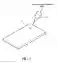
FIG. 1 shows a sealing membrane where a thermal interface material is injected therein according to aspects of the present disclosure.
FIG. 2 is a cross-sectional view of a semi-finished flip chip ball grid array package having a sealing membrane according to aspects of the present disclosure.
FIG. 3 is a cross-sectional view of a semi-finished flip chip ball grid array package having a plurality of sealing membranes for multiple chip module (MCM) packaging according to aspects of the present invention.
DETAILED DESCRIPTIONIn the following description, numerous specific details are set forth to provide a thorough understanding of the present invention. However, one having an ordinary skill in the art will recognize that the invention can be practiced without these specific details. In some instances, well-known structures and processes have not been described in detail to avoid unnecessarily obscuring the present invention.
Reference will now be made in detail to the present preferred embodiments of the present invention, examples of which are illustrated in the accompanying drawings.
Referring to FIG. 1, a sealing membrane 2 adapted for containing a thermal interface material 8 is shown. The thermal interface material 8 may be injected or delivered to the sealing membrane 2 by way of an injector or pump 6. Injector 6 may be any type injector adapted for delivering thermal interface material 8 to sealing membrane 2 and in one embodiment, may deliver the thermal interface material 8 through an orifice or a series of orifices 4 in sealing membrane 2.
Thermal interface material 8 performs a critical function of transferring heat generated by a die to a heat spreader which then spreads this heat to a heat sink. Thermal interface material 8 may have a modulus of elasticity in the range of about 1 to 500 MPA and be any type of thermally conductive material capable of being delivered to sealing membrane 2. Thermal interface material 8 may be, for example, a thermal grease, gel, polymer, or one of several epoxies.
Referring now to FIG. 2, illustrated is a side view diagram of a semi-finished flip chip ball grid array (FCBGA) package 10 having a sealing membrane 2 according to one embodiment of the present invention. FCBGA package 10 includes a semiconductor device 30 such as an integrated circuit chip (hereinafter referred to as chip 30). Chip 30 has an upper surface 32 and a lower surface 34 opposite the upper surface 32. A first set of solder balls 40 (or solder bumps) is connected to contact pads (not shown) on the lower surface 34 of chip 30. The combination of the chip 30 and the solder balls 40 are commonly known as and referred to as a flip chip. Chip 30 is secured to a first substrate 20 underlying chip 30. First substrate 20 may be an inorganic substrate and may include for example, a ceramic containing substrate such as Al2O3. Solder balls 40 are attached to contact pads (not shown) on the upper surface of first substrate 20. Although solder balls 40 are employed to couple chip 30 to first substrate 20, any means for coupling the chip to the substrate are within the scope of the present disclosure. FIG. 2 also shows an underfill 50 which may be filled between chip 30 and first substrate 20.
A second set of solder balls 60 may be secured to contact pads (not shown) on the lower surface of first substrate 20. The combination of the first substrate 20 and the second set of solder balls 60 on the lower surface thereof are commonly known as and referred to as a ball grid array. Second set of solder balls 60 may also be secured to contact pads (not shown) on a second substrate 70, which may be a printed wire board (also sometimes called a printed circuit board) or may be a multilayer module known to those skilled in the art.
The FCBGA package 10 may also include a heat spreader 80 and one or more stiffeners 90 for preventing excess warpage of the FCBGA package 10. Heat spreader 80 is mounted on top of chip 30 and counter-balances the forces exerted by the thermal expansion mismatches between at least the chip 30 and the first substrate 20. The heat spreader 80 and the stiffeners 90 may be formed integrally or employed as discrete elements, and may substantially comprise materials having relatively high coefficients of thermal expansion. In one embodiment, the heat spreader 80 comprises copper tungsten, aluminum silicon carbide, aluminum, stainless steel, copper, nickel and/or nickel-plated copper. In one embodiment, the stiffener 90 comprises copper, copper carbon, copper tungsten, aluminum silicon carbide, aluminum, stainless steel, nickel and/or nickel-plated copper. Other materials may be implemented accordingly to meet the design requirements of a particular application and the heat spreader 80 and the stiffener 90 may comprise other materials having high coefficients of thermal expansion as is known to those skilled in the art. However, in one embodiment, heat spreader 80, stiffener 90 may have substantially equal coefficients of thermal expansion, due to substantial similarities of the materials selected for each element.
Further illustrated in FIG. 2, the FCBGA package 10 may include thermal adhesive 100. The thermal adhesive may be disposed between the heat spreader 80 and the stiffeners 90, or between the first substrate 20 and the stiffeners 90, or both. The thermal adhesive 100 may comprise a viscous gel or liquid material, such as thermal grease, silver paste or solder. Thermal adhesive 100 may be applied in the form of a thin layer applied by mechanical layer spreading. Alternatively, thermal adhesive 100 may be applied by capillary action.
In one embodiment, heat spreader 80 has substantially similar dimensions as first substrate 20, although in other embodiments heat spreader 80 may be substantially smaller than first substrate 20. In either case, heat spreader 80 may be sized to substantially cover and enclose first substrate 20 in conjunction with the stiffeners 90. Accordingly, heat spreader 80 and stiffeners 90 may define a cavity 110 within which chip 30 is coupled to the first substrate 20. In one embodiment, the cavity 110 may be substantially filled with a thermo-set epoxy or other underfill material 50 by means known to those skilled in the art.
Also shown in FIG. 2, the FCBGA package 10 includes a sealing membrane 2 disposed between the chip 30 and the heat spreader 80. Sealing membrane 2 containing a thermal interface material 8 transmits the heat generated from chip 30 to heat spreader 80 and protects the FCBGA package 10 from flexural damage. Sealing membrane 2 reduces the warpage of FCBGA package 10 caused by thermal expansion mismatches between at least the chip 30, first substrate 20, and underfill 50. Sealing membrane 2 has substantial flexibility yet maintains dimensional stability and in one embodiment, sealing membrane 2 includes a material, shape, and a thickness that may be adjusted to match the coefficient of thermal expansion of the chip 30, the substrate 20 and the heat spreader 80 as is known to those skilled in the art. By dissipating the stress between the chip 30 and the heat spreader 80, sealing membrane 2 prevents interfacial delaminations at the interfaces of the sealing membrane 2 with the chip 30 and the heat spreader 80. Further, sealing membrane 2 conforms well to surface irregularities upon being disposed on chip 30 and/or the heat spreader 80 and sandwiched therebetween during assembling of the semiconductor package. In one embodiment, sealing membrane may be secured to the upper surface of chip 30 by an adhesive (not shown) such as, for example epoxy. The adhesive may be chosen to match or accommodate the coefficients of thermal expansion of the sealing membrane 2 and chip 30.
Sealing membrane 2 may comprise one or more layers and is so dimensioned as to be insertable through the space between the chip 30 and the heat spreader 80. Sealing membrane 2 comprises a flexible yet high heat transferring material and in one embodiment, sealing membrane 2 comprises silicon rubber. However, one skilled in the art will understand that sealing membrane 2 may comprise of any material having substantial flexibility, high heat emissive capacity yet maintain dimensional stability. In one embodiment, sealing membrane 2 may have a bulk thermal conductivity of 0.1 to 0.3 W/mk and have a flexural modulus less than about 1000 MPa.
Sealing membrane 2 may have a shape comprising of, for example, a rectangle, square, circle, rhombus, ellipse, or polygon but it is understood by those skilled in the art that the shape is dependent on at least the size and shape of the chip 30. The larger the chip is, the larger the sealing membrane size must be to adequately dissipate heat and withstand the package warpage and/or the fabrication process. Other shapes and configurations may be implemented accordingly to meet the design criteria of a particular application. Although FIG. 2 shows that sealing membrane 2 is implemented in a FCBGA package, it is understood by those skilled in the art that sealing membrane 2 may be implemented in any type of semiconductor package according to design criteria.
The thermal interface material for use in the sealing membrane 2 may be, for example, a thermal grease, gel, polymer, or one of several epoxies. In one embodiment, the thermal interface material comprises a conductive material such as aluminum, copper, carbon compound, aluminum compound, silver, or combinations thereof
Aspects of the present invention may be used in other semiconductor packaging, such as multiple chip module (MCM). FIG. 3 is a cross-sectional view of a semi-finished flip chip ball grid array package having a plurality of sealing membranes for multiple chip module (MCM) packaging according to aspects of the present invention. The plurality of sealing membranes 1, 2, and 3 as shown in FIG. 3 are connected to each other by a wire, such as for example a plastic wire.
In the preceding detailed description, the present invention is described with reference to specifically exemplary embodiments thereof It will, however, be evident that various modifications, structures, processes, and changes may be made thereto without departing from the broader spirit and scope of the present invention, as set forth in the claims. The specification and drawings are, accordingly, to be regarded as illustrative and not restrictive. It is understood that the present invention is capable of using various other combinations and environments and is capable of changes or modifications within the scope of the inventive concept as expressed herein.
Claims
What is claimed is:1. A semiconductor package comprising:
a semiconductor die;
a heat spreader; and
a sealed membrane for containing a thermal interface material (TIM) therein, the sealed membrane located between the die and the heat spreader for transmitting heat generated from the die to the heat spreader.
2. The semiconductor package of claim 1, further comprising a substrate above which the die, sealed membrane, and the heat spreader are mounted.
3. The semiconductor package of claim 1, further comprising a substrate, and wherein the die is a flip chip mounted above the substrate.
4. The semiconductor package of claim 1, wherein the sealed membrane has substantial flexibility yet maintains dimensional stability.
5. The semiconductor package of claim 2, wherein the sealed membrane includes a material, shape, and a thickness that may be adjusted to match the coefficient of thermal expansion of the die, substrate, and heat spreader.
6. The semiconductor package of claim 1, wherein the sealed membrane is so dimensioned as to be insertable through the space between the die and the heat spreader.
7. The semiconductor package of claim 1, wherein the sealed membrane is placed on the die with an adhesive.
8. The semiconductor package of claim 1, wherein the sealed membrane includes at least one orifice for delivering the thermal interface material thereto.
9. The semiconductor package of claim 1, wherein the sealed membrane has a bulk thermal conductivity of 0.1 to 0.3 W/mk.
10. The semiconductor package of claim 1, wherein the sealed membrane has a flexural modulus less than about 1000 MPA
11. The semiconductor package of claim 1, wherein the sealed membrane comprises silicon rubber.
12. The semiconductor package of claim 1, wherein the thermal interface material is a conductive material selected from the group consisting of aluminum, copper, carbon compound, aluminum compound, silver, or combinations thereof.
13. A method for forming a semiconductor package, comprising:
providing a semiconductor die;
providing a heat spreader;
providing a sealed membrane for containing a thermal interface material therein; and
assembling the sealed membrane between the die and the heat spreader.
14. The method of claim 13 further comprising mounting the die, sealed membrane, and heat spreader above a substrate.
15. The method of claim 13, wherein the die is a flip chip mounted above a substrate.
16. The method of claim 13, wherein the sealed membrane has substantial flexibility yet maintains dimensional stability.
17. The method of claim 13, wherein the sealed membrane is so dimensioned as to be insertable through the space between the die and the heat spreader.
18. The method of claim 13, wherein the sealed membrane is placed on the die with an adhesive.
19. The method of claim 13, wherein the sealed membrane includes at least one orifice for delivering the thermal interface material thereto.
20. The method of claim 13, wherein the sealed membrane comprises silicon rubber.
21. The method of claim 13, wherein the thermal interface material is a conductive material selected from the group consisting of aluminum, copper, carbon compound, aluminum compound, silver, or combinations thereof.
22. A method of dissipating heat from a semiconductor package, comprising:
transferring heat from a semiconductor die in the semiconductor package to a heat spreader with a sealed membrane containing a thermal interface material therein, the sealed membrane located between the die and the heat spreader.
23. The method of claim 22, wherein the sealed membrane has substantial flexibility yet maintains dimensional stability.
24. The method of claim 22, wherein the sealed membrane is so dimensioned as to be insertable through the space between the die and the heat spreader.
25. The method of claim 22, wherein the sealed membrane is placed on the die with an adhesive.
26. The method of claim 22, wherein the sealed membrane includes at least one orifice for delivering the thermal interface material thereto.
27. The method of claim 22, wherein the sealed membrane comprises silicon rubber.
28. The method of claim 22, wherein the thermal interface material is a conductive material selected from the group consisting of aluminum, copper, carbon compound, aluminum compound, silver, or combinations thereof.
Images & Drawings included:


Sources:
- United States Patent and Trademark Office - verify current appl. status at the USPTO↗
Recent applications in this class:
- » 20240282667 2024-08-22
Enhanced base die heat path using through-silicon vias - » 20240234246 2024-07-11
INTEGRATED CIRCUIT DIRECT COOLING SYSTEMS AND RELATED METHODS - » 20240222222 2024-07-04
Embedded liquid cooling - » 20240186218 2024-06-06
MOLDED POWER MODULES WITH FLUIDIC-CHANNEL COOLED SUBSTRATES - » 20240105550 2024-03-28
Water Cooling System for Semiconductor Package - » 20240014100 2024-01-11
Coplanar control for film-type thermal interface - » 20240006268 2024-01-04
PACKAGE STRUCTURE AND METHOD OF FABRICATING THE SAME - » 20240006267 2024-01-04
Hermetic Package Cooling Using Silver Tubes with Getter Absorption Material - » 20230290707 2023-09-14
Apparatus And Method To Reduce The Thermal Resistance Of Semiconductor Substrates - » 20230197566 2023-06-22
Semiconductor Die, Heat Spreader, Semiconductor Package, Semiconductor Device, and Methods