Assembly of a semiconductor die attached to substrate with oxazoline derivative bearing an electron donor or acceptor functionality
US20060263928A1
2006-11-23
10/555,291
2004-02-17
✅ Patent granted
US 7,528,404 B2
2009-05-05
WO; PCT/US2004/004736; 20040217
WO; WO2005/083771; 20050909
Jerome Jackson | Anthony Ho
2025-02-13
Abstract:
An assembly of a semiconductor die attached to a substrate is made with a composition comprising compounds that contain an oxazoline functionality and an electron acceptor or an electron donor functionality. Electron donor functionalities include styrenic, cinnamyl, and vinyl ether groups. Electron acceptor functionalities include maleimide, acrylate, fumarate, and maleate groups. An exemplary compound has the structure: formula (I).
Inventors:
- Ruzhi ZHANG 16 🇺🇸 Pennington, NJ, United States
- Osama M. Musa 46 🇺🇸 Hillsborough, NJ, United States
- Rushi Zhang 1 🇺🇸 Pennington, NJ, United States
Assignee:
- Henkel AG & Co. KGaA 109 🇩🇪 Düsseldorf, Germany
Interested in similar patents?
Get notified when new applications in this technology area are published.
Classification:
C07D263/10 » CPC main
Heterocyclic compounds containing 1,3-oxazole or hydrogenated 1,3-oxazole rings not condensed with other rings having one double bond between ring members or between a ring member and a non-ring member with only hydrogen atoms, hydrocarbon or substituted hydrocarbon radicals, directly attached to ring carbon atoms
C07D263/14 » CPC further
Heterocyclic compounds containing 1,3-oxazole or hydrogenated 1,3-oxazole rings not condensed with other rings having one double bond between ring members or between a ring member and a non-ring member with only hydrogen atoms, hydrocarbon or substituted hydrocarbon radicals, directly attached to ring carbon atoms with radicals substituted by oxygen atoms
C07D413/12 » CPC further
Heterocyclic compounds containing two or more hetero rings, at least one ring having nitrogen and oxygen atoms as the only ring hetero atoms containing two hetero rings linked by a chain containing hetero atoms as chain links
C08G61/00 » CPC further
Macromolecular compounds obtained by reactions forming a carbon-to-carbon link in the main chain of the macromolecule
C08G61/02 » CPC further
Macromolecular compounds obtained by reactions forming a carbon-to-carbon link in the main chain of the macromolecule Macromolecular compounds containing only carbon atoms in the main chain of the macromolecule, e.g. polyxylylenes
C08G73/02 » CPC further
Macromolecular compounds obtained by reactions forming a linkage containing nitrogen with or without oxygen or carbon in the main chain of the macromolecule, not provided for in groups - Polyamines
H01L21/563 » CPC further
Processes or apparatus adapted for the manufacture or treatment of semiconductor or solid state devices or of parts thereof; Manufacture or treatment of semiconductor devices or of parts thereof the devices having at least one potential-jump barrier or surface barrier, e.g. PN junction, depletion layer or carrier concentration layer; Assembly of semiconductor devices using processes or apparatus not provided for in a single one of the subgroups - , e.g. sealing of a cap to a base of a container; Encapsulations, e.g. encapsulation layers, coatings Encapsulation of active face of flip-chip device, e.g. underfilling or underencapsulation of flip-chip, encapsulation preform on chip or mounting substrate
H01L23/293 » CPC further
Details of semiconductor or other solid state devices; Encapsulations, e.g. encapsulating layers, coatings, e.g. for protection characterised by the material, e.g. carbon Organic, e.g. plastic
H01L24/29 » CPC further
Arrangements for connecting or disconnecting semiconductor or solid-state bodies; Methods or apparatus related thereto; Means for bonding being attached to, or being formed on, the surface to be connected, e.g. chip-to-package, die-attach, "first-level" interconnects; Manufacturing methods related thereto; Layer connectors, e.g. plate connectors, solder or adhesive layers; Manufacturing methods related thereto; Structure, shape, material or disposition of the layer connectors prior to the connecting process of an individual layer connector
H01L24/83 » CPC further
Arrangements for connecting or disconnecting semiconductor or solid-state bodies; Methods or apparatus related thereto; Methods for connecting semiconductor or other solid state bodies using means for bonding being attached to, or being formed on, the surface to be connected using a layer connector
H01L2224/29 » CPC further
Indexing scheme for arrangements for connecting or disconnecting semiconductor or solid-state bodies and methods related thereto as covered by; Means for bonding being attached to, or being formed on, the surface to be connected, e.g. chip-to-package, die-attach, "first-level" interconnects; Manufacturing methods related thereto; Layer connectors, e.g. plate connectors, solder or adhesive layers; Manufacturing methods related thereto; Structure, shape, material or disposition of the layer connectors prior to the connecting process of an individual layer connector
H01L2224/73203 » CPC further
Indexing scheme for arrangements for connecting or disconnecting semiconductor or solid-state bodies and methods related thereto as covered by; Means for bonding being of different types provided for in two or more of groups; Location after the connecting process on the same surface Bump and layer connectors
H01L2224/8385 » CPC further
Indexing scheme for arrangements for connecting or disconnecting semiconductor or solid-state bodies and methods related thereto as covered by; Methods for connecting semiconductor or other solid state bodies using means for bonding being attached to, or being formed on, the surface to be connected using a layer connector; Bonding techniques using a polymer adhesive, e.g. an adhesive based on silicone, epoxy, polyimide, polyester
H01L2924/01005 » CPC further
Indexing scheme for arrangements or methods for connecting or disconnecting semiconductor or solid-state bodies as covered by; Chemical elements Boron [B]
H01L2924/01006 » CPC further
Indexing scheme for arrangements or methods for connecting or disconnecting semiconductor or solid-state bodies as covered by; Chemical elements Carbon [C]
H01L2924/01011 » CPC further
Indexing scheme for arrangements or methods for connecting or disconnecting semiconductor or solid-state bodies as covered by; Chemical elements Sodium [Na]
H01L2924/01013 » CPC further
Indexing scheme for arrangements or methods for connecting or disconnecting semiconductor or solid-state bodies as covered by; Chemical elements Aluminum [Al]
H01L2924/01015 » CPC further
Indexing scheme for arrangements or methods for connecting or disconnecting semiconductor or solid-state bodies as covered by; Chemical elements Phosphorus [P]
H01L2924/0102 » CPC further
Indexing scheme for arrangements or methods for connecting or disconnecting semiconductor or solid-state bodies as covered by; Chemical elements Calcium [Ca]
H01L2924/01029 » CPC further
Indexing scheme for arrangements or methods for connecting or disconnecting semiconductor or solid-state bodies as covered by; Chemical elements Copper [Cu]
H01L2924/01046 » CPC further
Indexing scheme for arrangements or methods for connecting or disconnecting semiconductor or solid-state bodies as covered by; Chemical elements Palladium [Pd]
H01L2924/01047 » CPC further
Indexing scheme for arrangements or methods for connecting or disconnecting semiconductor or solid-state bodies as covered by; Chemical elements Silver [Ag]
H01L2924/0105 » CPC further
Indexing scheme for arrangements or methods for connecting or disconnecting semiconductor or solid-state bodies as covered by; Chemical elements Tin [Sn]
H01L2924/01056 » CPC further
Indexing scheme for arrangements or methods for connecting or disconnecting semiconductor or solid-state bodies as covered by; Chemical elements Barium [Ba]
H01L2924/01078 » CPC further
Indexing scheme for arrangements or methods for connecting or disconnecting semiconductor or solid-state bodies as covered by; Chemical elements Platinum [Pt]
H01L2924/01079 » CPC further
Indexing scheme for arrangements or methods for connecting or disconnecting semiconductor or solid-state bodies as covered by; Chemical elements Gold [Au]
H01L2924/01082 » CPC further
Indexing scheme for arrangements or methods for connecting or disconnecting semiconductor or solid-state bodies as covered by; Chemical elements Lead [Pb]
H01L2924/07802 » CPC further
Indexing scheme for arrangements or methods for connecting or disconnecting semiconductor or solid-state bodies as covered by; Polymers; Adhesive characteristics other than chemical not being an ohmic electrical conductor
H01L2924/04642 » CPC further
Indexing scheme for arrangements or methods for connecting or disconnecting semiconductor or solid-state bodies as covered by; Carbides composed of metals from groups of the periodic table 14th Group SiC
H01L2924/0503 » CPC further
Indexing scheme for arrangements or methods for connecting or disconnecting semiconductor or solid-state bodies as covered by; Nitrides composed of metals from groups of the periodic table 13th Group
H01L2924/05432 » CPC further
Indexing scheme for arrangements or methods for connecting or disconnecting semiconductor or solid-state bodies as covered by; Oxides composed of metals from groups of the periodic table 13th Group AlO
H01L2924/0665 » CPC further
Indexing scheme for arrangements or methods for connecting or disconnecting semiconductor or solid-state bodies as covered by; Polymers Epoxy resin
H01L2924/00014 » CPC further
Indexing scheme for arrangements or methods for connecting or disconnecting semiconductor or solid-state bodies as covered by; Technical content checked by a classifier the subject-matter covered by the group, the symbol of which is combined with the symbol of this group, being disclosed without further technical details
H01L2924/014 » CPC further
Indexing scheme for arrangements or methods for connecting or disconnecting semiconductor or solid-state bodies as covered by; Alloys Solder alloys
H01L2224/29099 » CPC further
Indexing scheme for arrangements for connecting or disconnecting semiconductor or solid-state bodies and methods related thereto as covered by; Means for bonding being attached to, or being formed on, the surface to be connected, e.g. chip-to-package, die-attach, "first-level" interconnects; Manufacturing methods related thereto; Layer connectors, e.g. plate connectors, solder or adhesive layers; Manufacturing methods related thereto; Structure, shape, material or disposition of the layer connectors prior to the connecting process of an individual layer connector; Core members of the layer connector Material
H01L2924/00013 » CPC further
Indexing scheme for arrangements or methods for connecting or disconnecting semiconductor or solid-state bodies as covered by; Technical content checked by a classifier Fully indexed content
H01L2924/10253 » CPC further
Indexing scheme for arrangements or methods for connecting or disconnecting semiconductor or solid-state bodies as covered by; Details of semiconductor or other solid state devices to be connected; Material of the semiconductor or solid state bodies; Semiconducting materials; Elemental semiconductors, i.e. Group IV Silicon [Si]
H01L2924/00 » CPC further
Indexing scheme for arrangements or methods for connecting or disconnecting semiconductor or solid-state bodies as covered by
H01L21/00 IPC
Processes or apparatus adapted for the manufacture or treatment of semiconductor or solid state devices or of parts thereof
H01L23/02 IPC
Details of semiconductor or other solid state devices Containers; Seals
H01L29/08 IPC
Semiconductor devices adapted for rectifying, amplifying, oscillating or switching, or capacitors or resistors with at least one potential-jump barrier or surface barrier, e.g. PN junction depletion layer or carrier concentration layer; Details of semiconductor bodies or of electrodes thereof; Multistep manufacturing processes therefor; Semiconductor bodies ; Multistep manufacturing processes therefor characterised by their shape; characterised by the shapes, relative sizes, or dispositions of the semiconductor regions ; characterised by the concentration or distribution of impurities within semiconductor regions with semiconductor regions connected to an electrode carrying current to be rectified, amplified or switched and such electrode being part of a semiconductor device which comprises three or more electrodes
H01L35/24 IPC
Thermoelectric devices comprising a junction of dissimilar materials, i.e. exhibiting Seebeck or Peltier effect with or without other thermoelectric effects or thermomagnetic effects; Processes or apparatus peculiar to the manufacture or treatment thereof or of parts thereof; Details thereof; Selection of the material for the legs of the junction using organic compositions
H01L51/00 IPC
Solid state devices using organic materials as the active part, or using a combination of organic materials with other materials as the active part; Processes or apparatus specially adapted for the manufacture or treatment of such devices, or of parts thereof
Description
FIELD OF THE INVENTIONThis invention relates to an assembly of a semiconductor die attached to a substrate with a curable or cured composition that contains a compound having both oxazoline functionality and electron acceptor or electron donor functionality.
BACKGROUND OF THE INVENTIONThe fabrication of semiconductor packages and microelectronic devices call for the use of adhesive and encapsulant compositions in assembly processes. Typical compositions include radical-curable compositions and electron donor/electron acceptor systems. These do not always give optimum performance in certain uses and there is still a need for performance materials within the semiconductor fabrication industry.
SUMMARY OF THE INVENTIONThis invention is directed to an assembly of a semiconductor die attached to or supported on a substrate with a composition comprising a compound that contains an oxazoline functionality and an electron acceptor or an electron donor functionality. The composition is applied in a curable state and cured in situ. Electron donor functionalities include styrenic, cinnamyl, and vinyl ether groups. Electron acceptor functionalities include maleimide, acrylate, fumarate, and maleate groups.
DETAILED DESCRIPTION OF THE INVENTIONOxazolines are five-membered heterocyclic compounds having a nitrogen atom, an oxygen atom, and one double bond. The double bond may be located in one of the three positions, making possible the existence of three different oxazoline rings: 2-oxazolines (most common), 3-oxazolines, and 4-oxazolines. Oxazolines undergo cationic ring opening homopolymerization; electron donor/electron acceptor systems undergo free radical polymerization. Thus, compounds having at least one oxazoline group and one electron donor or electron acceptor functionality per molecule have the capability of undergoing dual cure, both thermal and radiation.
The compositions used herein comprise a compound having oxazoline and electron donor or electron acceptor functionalities, curing agent and filler. In those compositions in which an electron acceptor functionality is present, the curing agent is optional. The composition can be a paste, prepared by blending or milling, or can be a film, prepared by standard film making techniques known to those skilled in the art.
The composition will consist mainly of the compound having oxazoline and electron donor or electron acceptor functionalities; alternatively, the compound having oxazoline and electron donor or electron acceptor functonalities can be used in a lesser amount as an adhesion promoter to one or more other curable resins. When used as an adhesion promoter, the amount used in the composition will be an effective amount and will range from 0.005 to 20.0 percent by weight of the formulation.
When used as an adhesion promoter, the main component will be any other suitable curable resin, including, for example, epoxy, vinyl ether, thiolene, a resin derived from cinnamyl and styrenic starting compounds, fumarate, maleate, acrylate, maleimide, cyanate ester, oxetane, phenol, amino resin, propargyl ether, benzocyclobutene, and benzoxazine.
Suitable curing agents are thermal initiators and photoinitiators present in an effective amount to cure the composition. In general, those amounts will range from 0.1% to 30%, preferably 1% to 20%, by weight of the total organic material (that is, excluding any inorganic fillers) in the composition.
Preferred radical initiators include peroxides, such as butyl peroctoates and dicumyl peroxide, and azo compounds, such as 2,2′-azobis(2-methyl-propanenitrile) and 2,2′-azobis(2-methyl-butanenitrile). Preferred cabonic initiators include iodonium, oxonium, sulfonium, sulfoxonium, and various other onium salts. Other suitable cationic initiators include Lewis acid catalysts and alkylation agents, such as, arlysulfonate esters, e.g., methyl-p-toluenesuffonate and methyl trifluoromethanesulfonate. A preferred series of photoinitiators are those sold under the trademark Irgacure or Rhodorsil 2074 by Ciba Specialty Chemicals. In some formulations, both thermal initiation and photoinitiation may be desirable: the curing process can be started either by irradiation, followed by heat, or can be started by heat, followed by irradiation.
The curable compositions will cure within a temperature range of 60° C. to 250° C., and curing will be effected within a range of three seconds to three hours. The actual cure profile will vary with the components and can be determined without undue experimentation by the practitioner.
Suitable fillers can be conductive or nonconductive. Exemplary conductive fillers are carbon black, graphite, gold, silver, copper, platinum, palladium, nickel, aluminum, silicon carbide, boron nitride, diamond, and alumina. Exemplary nonconductive fillers are particles of vermiculite, mica, wollastonite, calcium carbonate, titania, sand, glass, fused silica, fumed silica, barium sulfate, and halogenated ethylene polymers, such as tetrafluoroethylene, trifluoro-ethylene, vinylidene fluoride, vinyl fluoride, vinylidene chloride, and vinyl chloride. Fillers generally will be present in amounts of 20% to 90% by weight of the formulation.
These compositions are useful for attaching semiconductor dies to substrates or for supporting a semiconductor die as an underfill between the die and substrate. Typical substrates are fabricated from metal, for example, copper, silver, gold, nickel, alloys (such as, 42Fe/58Ni alloy), silver-coated copper, or palladium-coated copper; from organic material, for example, polyimides, polyamides, or polyesters; from ceramic; and from composites or laminates (such as, printed wire boards).
In a typical die attach operation, the adhesive in paste or film form is placed onto the substrate, such as the center paddle of the leadframe, and the silicon die contacted to the adhesive with heat and pressure. The exact process and processing parameters may vary from operation to operation. These parameters and processes are known to those skilled in the art and are not meant to form a part of this invention.
In a typical underfill operation, connections are made between electrical terminals on the die and corresponding electrical terminals on the substrate using metallic or polymeric solder. A bump of solder is placed on the terminals of the substrate, the terminals are aligned and contacted, and the resulting assembly heated to reflow the solder. A gap is created between the die and the substrate, which is filled with a polymeric encapsulant or underfill to reinforce the interconnect. There are variations in the processes for the underfill, for example, the underfill encapsulation may take place after the reflow of the solder or simultaneously with the reflow of the solder. These processes are known to those skilled in the art and are not meant to form a part of this invention.
The gist of this invention is the use of the oxazoline compounds as a die attach or underfill encapsulant for attaching or suppporting semiconductor dies to substrates.
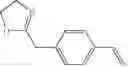
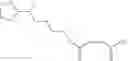
Various synthetic routes to the oxazoline compounds can be devised with reference to the following synthetic schemes. To prepare a compound having both styrenic and oxazoline functionality such as
a procedure according to A. Zerroukhi, A. Ainser, A. Arsac, N. Mignard, and B. Marculescu, Polymer Bulletin, 42, 535, 1999, is used. Initially, vinylbenzyl chloride is reacted with sodium cyanide to give vinylbenzyl cyanide, which is then reacted with ethanolamine to give the vinylbenzyloxazoline.
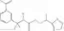
To prepare a compound having both maleimide and oxazoline functionality such as
maleic anhydride (in acetonitrile) is reacted with 6-aminocaprioc acid (in acetic acid) to form the amic acid adduct. The adduct is dehydrated to close the ring and form the maleimide. Procedures for this reaction are known in the art. The product, 6-maleimidocaproic acid, is then reacted with 2-(3-hydroxy-2-propyl)-2-oxazoline (in toluene heated to 80° C.) with a catalytic amount of sulfuric acid, worked up, and the product isolated.
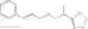
To prepare a compound having both cinnamyl and oxazoline functionality such as
2-(3-hydroxy-2-propyl)-2-oxazoline in an excess amount of 50% NaOH and a catalytic amount of tetrabutyl ammonium hydrogen sulfate is reacted with cinnamyl chloride in toluene for several hours first at 53° C., then at 75° C. The reaction is allowed to cool to room temperature and the organic layer extracted and washed with brine three times. The isolated organic layer is dried over MgSO4, filtered and the solvent removed in vacuo to give the product.
To prepare a compound having both styrenic and oxazoline functionality such as
3-isopropenyl-α,α-dimethylbenzyl isocyanate (m-TMI) and 2-(3-hydroxy-2-propyl)-2-oxazoline are solvated in toluene and reacted under nitrogen with a catalytic amount of dibutyltin dilaurate at 60° C. for several hours. After the reaction is allowed to cool to room temperature, the solvent is removed in vacuo to give the product.
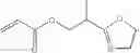
To prepare a compound having both acrylate and oxazoline functionality such as
2-(3-hydroxy-2-propyl)-2-oxazoline and triethylamine are mixed in dry methylene chloride at 0° C. The appropriate equivalent of acryloyl chloride dissolved in dry methylene chloride is carefully added and the mixture allowed to react for several hours. The solvent is evaporated and the crude product is purified by column chromatography using a gradient of hexane/ethyl acetate.
To prepare a compound having both vinyl ether and oxazoline functionality such as
2-(3-hydroxy-2-propyl)-2-oxazoline in an excess amount of 50% NaOH and a catalytic amount of tetrabutyl ammonium hydrogen sulfate is reacted with 2-chloroethyl vinyl ether in toluene for several hours, first at 53° C., then at 75° C. The reaction is allowed to cool to room temperature and the organic layer extracted and washed with brine three times. The isolated organic layer is dried over MgSO4, filtered, and the solvent removed in vacuo to give the product.
To prepare a compound having both maleate and oxazoline functionality such as
2-isopropenyl-2-oxazoline and 2-mercaptoethanol are reacted in toluene at 70° C. A solution of azodiisobutyronitrile (AIBN) in toluene is added to the mixture, and the reaction continued at 70° C. for several hours. The 2-isopropenyl-2-oxazoline/2-mercaptoethanol adduct is obtained after removal of the solvent under reduced pressure. This 2-isopropenyl-2-oxazoline/2-mercaptoethanol adduct is then reacted under nitrogen with maleic anhydride in 300 mL of dimethoxyethane at 70° C. for one hour. After cooling, the contents of the reaction are poured into heptane. The resulting product is dried at 40° C. in vacuo for 24 hours.
Claims
What is claimed:1. An assembly of a semiconductor die attached to a substrate with a composition comprising a compound having an oxazoline functionality and an electron acceptor or electron donor functionality.
2. The assembly according to claim 1 in which the electron donor functionalities are selected from the group consisting of styrenic, cinnamyl, and vinyl ether.
3. The assembly according to claim 1 in which the electron acceptor functionalities are selected from the group consisting of maleimide, acrylate, fumarate, and maleate groups.
4. The assembly according to claim 1 in which the compound having an oxazoline functionality and an electron acceptor or an electron donor functionality contains an electron donor functionality and has the structure
5. The assembly according to claim 1 in which the compound having an oxazoline functionality and an electron acceptor or electron donor functionality contains an electron acceptor functionality and has the structure
6. The assembly according to claim 1 in which the compound having an oxazoline functionality and an electron acceptor or electron donor functionality contains an electron donor functionality and has the structure
7. The assembly according to claim 1 in which the compound having an oxazoline functionality and an electron acceptor or electron donor functionality contains an electron donor functionality and has the structure
8. The assembly according to claim 1 in which the compound having an oxazoline functionality and an electron acceptor or electron donor functionality contains an electron acceptor functionality and has the structure
9. The assembly according to claim 1 in which the compound having an oxazoline functionality and an electron acceptor or electron donor functionality contains an electron donor functionality and has the structure
10. The assembly according to claim 1 in which the compound having an oxazoline functionality and an electron acceptor or electron donor functionality contains an electron acceptor functionality and has the structure
Images & Drawings included:


Sources:
- United States Patent and Trademark Office - verify current appl. status at the USPTO↗
Recent applications in this class:
- » 20120083562 2012-04-05
Polymer-filler coupling additives - » 20100305316 2010-12-02
Processes for preparing (R)-8-chloro-1-methyl-2,3,4,5-tetrahydro-1H-3-benzazepine and intermediates thereof - » 20100076186 2010-03-25
Process for preparing heterocycles - » 20070161756 2007-07-12
Polymer-filler coupling additives - » 20050203144 2005-09-15
Bicyclo[3.1.0]hexane containing oxazolidinone antibiotics and derivatives thereof - » 20050181948 2005-08-18
Phenethylacrylamide, methods for the production thereof and agents containing the same - » 20050090498 2005-04-28
3-Quinolin-2(1h)-ylideneindolin-2-one derivative - » 15604377 2019-04-23
Sulfoxide ligand metal catalyzed oxidation of olefins
Recent applications for this Assignee:
- » 20240199988 2024-06-20
POWDERED DETERGENT COMPOSITION - » 20240165011 2024-05-23
METHOD FOR DYEING KERATINOUS MATERIAL, COMPRISING THE USE OF AN ORGANOSILICON COMPOUND, A DYEING COMPOUND, A SEALING REAGENT, AND A POLYMER-CONTAINING POST-TREATMENT AGENT - » 20240067899 2024-02-29
Dissolvable toilet brush formulations with desiccant and free of cohesion polymer - » 20240067898 2024-02-29
Dissolvable toilet brush formulations with desiccant and dye system to indicate cleaning - » 20240067897 2024-02-29
Dissolvable toilet brush formulations containing polyethylene glycol - » 20230210337 2023-07-06
Cleaning device with gripping assembly for a dissolvable cleaning head - » 20230046332 2023-02-16
Toilet cleaning product containing aqueous crystalline material - » 20220073843 2022-03-10
Systems and methods of forming and analyzing dissolvable articles - » 20220033746 2022-02-03
Unit dose packs with anti-efflorescence formulations - » 20220002068 2022-01-06
Packaging System For At Least One Product Preparation Component And Corresponding Method For Handling The Product Preparation Component