Integrated circuit package substrate having a thin film capacitor structure
US20060270111A1
2006-11-30
11/494,354
2006-07-26
✅ Patent granted
US 7,504,271 B2
2009-03-17
-
-
George Fourson
2027-04-07
Abstract:
This invention relates to the manufacture of a substrate, such as a package substrate or an interposer substrate, of an integrated circuit package. A base structure is formed from a green material having a plurality of via openings therein. The green material is then sintered so that the green material becomes a sintered ceramic material and the base structure becomes a sintered ceramic base structure having the via openings. A conductive via is formed in each via opening of the sintered ceramic base structure. A capacitor structure is formed on the sintered ceramic base structure. The power and ground planes of the capacitor structure are connected to the vias. As such, a capacitor structure can be formed and connected to the vias without the need to drill vias openings in brittle substrates such as silicon substrates. The sintered ceramic material also has a low coefficient of thermal expansion and can resist high temperature processing conditions when manufacturing the capacitor structure, and is inexpensive to manufacture.
Assignee:
- INTEL CORPORATION 47,158 🇺🇸 Santa Clara, CA, United States
Interested in similar patents?
Get notified when new applications in this technology area are published.
Classification:
H05K1/162 » CPC main
Printed circuits incorporating printed electric components, e.g. printed resistor, capacitor, inductor incorporating printed capacitors
H05K1/162 » CPC main
Printed circuits incorporating printed electric components, e.g. printed resistor, capacitor, inductor incorporating printed capacitors
H01L23/49822 » CPC further
Details of semiconductor or other solid state devices; Arrangements for conducting electric current to or from the solid state body in operation, e.g. leads, terminal arrangements ; Selection of materials therefor consisting of soldered constructions; Leads, on insulating substrates, Multilayer substrates
H01L23/642 » CPC further
Details of semiconductor or other solid state devices; Structural electrical arrangements for semiconductor devices not otherwise provided for, e.g. in combination with batteries; Impedance arrangements Capacitive arrangements
H01L2224/05573 » CPC further
Indexing scheme for arrangements for connecting or disconnecting semiconductor or solid-state bodies and methods related thereto as covered by; Means for bonding being attached to, or being formed on, the surface to be connected, e.g. chip-to-package, die-attach, "first-level" interconnects; Manufacturing methods related thereto; Bonding areas; Manufacturing methods related thereto; Structure, shape, material or disposition of the bonding areas prior to the connecting process of an individual bonding area; External layer Single external layer
H01L2224/16 » CPC further
Indexing scheme for arrangements for connecting or disconnecting semiconductor or solid-state bodies and methods related thereto as covered by; Means for bonding being attached to, or being formed on, the surface to be connected, e.g. chip-to-package, die-attach, "first-level" interconnects; Manufacturing methods related thereto; Bump connectors; Manufacturing methods related thereto; Structure, shape, material or disposition of the bump connectors after the connecting process of an individual bump connector
H01L2924/01019 » CPC further
Indexing scheme for arrangements or methods for connecting or disconnecting semiconductor or solid-state bodies as covered by; Chemical elements Potassium [K]
H01L2924/01078 » CPC further
Indexing scheme for arrangements or methods for connecting or disconnecting semiconductor or solid-state bodies as covered by; Chemical elements Platinum [Pt]
H01L2924/15174 » CPC further
Indexing scheme for arrangements or methods for connecting or disconnecting semiconductor or solid-state bodies as covered by; Details of package parts other than the semiconductor or other solid state devices to be connected; Die mounting substrate; Multilayer substrate; Fan-out arrangement of the internal vias in different layers of the multilayer substrate
H01L2924/15311 » CPC further
Indexing scheme for arrangements or methods for connecting or disconnecting semiconductor or solid-state bodies as covered by; Details of package parts other than the semiconductor or other solid state devices to be connected; Die mounting substrate; Connection portion the connection portion being formed only on the surface of the substrate opposite to the die mounting surface being a ball array, e.g. BGA
H05K1/0306 » CPC further
Printed circuits; Details; Use of materials for the substrate Inorganic insulating substrates, e.g. ceramic, glass
H05K1/0306 » CPC further
Printed circuits; Details; Use of materials for the substrate Inorganic insulating substrates, e.g. ceramic, glass
H05K3/4688 » CPC further
Apparatus or processes for manufacturing printed circuits; Manufacturing multilayer circuits Composite multilayer circuits, i.e. comprising insulating layers having different properties
H05K3/4688 » CPC further
Apparatus or processes for manufacturing printed circuits; Manufacturing multilayer circuits Composite multilayer circuits, i.e. comprising insulating layers having different properties
H05K2201/0187 » CPC further
Indexing scheme relating to printed circuits covered by; Dielectrics; Dielectric layers with regions of different dielectrics in the same layer, e.g. in a printed capacitor for locally changing the dielectric properties
H05K2201/0187 » CPC further
Indexing scheme relating to printed circuits covered by; Dielectrics; Dielectric layers with regions of different dielectrics in the same layer, e.g. in a printed capacitor for locally changing the dielectric properties
H05K2201/09309 » CPC further
Indexing scheme relating to printed circuits covered by; Shape and layout; Shape and layout details of conductors; Conductive planes Core having two or more power planes; Capacitive laminate of two power planes
H05K2201/09309 » CPC further
Indexing scheme relating to printed circuits covered by; Shape and layout; Shape and layout details of conductors; Conductive planes Core having two or more power planes; Capacitive laminate of two power planes
H01L2924/00014 » CPC further
Indexing scheme for arrangements or methods for connecting or disconnecting semiconductor or solid-state bodies as covered by; Technical content checked by a classifier the subject-matter covered by the group, the symbol of which is combined with the symbol of this group, being disclosed without further technical details
H01L2224/05599 » CPC further
Indexing scheme for arrangements for connecting or disconnecting semiconductor or solid-state bodies and methods related thereto as covered by; Means for bonding being attached to, or being formed on, the surface to be connected, e.g. chip-to-package, die-attach, "first-level" interconnects; Manufacturing methods related thereto; Bonding areas; Manufacturing methods related thereto; Structure, shape, material or disposition of the bonding areas prior to the connecting process of an individual bonding area; External layer Material
H01L21/00 IPC
Processes or apparatus adapted for the manufacture or treatment of semiconductor or solid state devices or of parts thereof
Description
CROSS-REFERENCE TO RELATED APPLICATIONSThis is a divisional of prior U.S. patent application Ser. No. 10/746,665, filed on Dec. 23, 2003.
This application is related to U.S. patent application Ser. No. 10/803,789 entitled “INTEGRATED CIRCUIT PACKAGE SUBSTRATE HAVING A THIN FILM CAPACITOR STRUCTURE,” by Palanduz, et al., filed on Mar. 17, 2004, which is hereby incorporated herein by reference.
BACKGROUND OF THE INVENTION1). Field of the Invention
This invention relates to a capacitor structure that is included in a substrate of an integrated circuit package.
2). Discussion of Related Art
Integrated circuits are usually manufactured on wafer substrates. Wafer substrate is then “diced” or “singulated” into individual dies, each die carrying a respective integrated circuit. The die is then mounted on a package substrate, often with an intermediate interposer substrate. The substrate or substrates provide structural rigidity to the resulting integrated circuit package. A package substrate also provides x-y transformation from contacts of the die to contacts on a carrier substrate on which the integrated circuit package is mounted.
Signals can be provided through conductors in the substrate or substrates to and from an integrated circuit in the die. Signal delay, referred to as resistance-capacitance-inductance delay, often occurs when signals are transmitted through the conductors. In order to reduce resistance-capacitance-inductance delay, a capacitor is often provided close to the die. The capacitor acts as a reservoir of power close to the integrated circuit.
Discrete capacitors are relatively large and thus take up a large amount of real estate on a substrate. It has been appreciated that thin film capacitors may take up less real estate, which will allow for more capacitors to be formed. It may also be simpler to manufacture thin film capacitors during the manufacture of a substrate than to mount discrete capacitors to a substrate.
Via openings have to be manufactured in a base structure of a substrate, in which conductive vias have to be formed to which power and ground planes of a thin film capacitor structure have to be connected. The formation of such via openings has been a preoccupation of the semiconductor industry for a number of years. Thus far, all efforts have been directed to drilling openings in low k-value materials such as silicon. Silicon is a brittle material, which makes it difficult to drill openings therein. Each opening also has to be drilled individually, which reduces throughput.
BRIEF DESCRIPTION OF THE DRAWINGSThe invention is described by way of examples with reference to the accompanying drawings wherein:
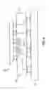
FIG. 1 is a cross-sectional side view of an interposer substrate manufactured according to an embodiment of the invention;
FIG. 2 is a cross-sectional side view of an integrated circuit package which includes the interposer substrate of FIG. 1;
FIG. 3 is a cross-sectional side view of a package substrate manufactured according to an embodiment of the invention; and
FIG. 4 is a cross-sectional side view of an integrated circuit package that includes the package substrate of FIG. 3.
DETAILED DESCRIPTION OF THE INVENTIONThe manufacture of a substrate, such as a package substrate or an interposer substrate, of an integrated circuit package is described. A base structure is formed from a green material having a plurality of via openings therein. The green material is then sintered so that the green material becomes a sintered ceramic material and the base structure becomes a sintered ceramic base structure having the via openings. A conductive via is formed in each via opening of the sintered ceramic base structure. A capacitor structure is formed on the sintered ceramic base structure. The power and ground planes of the capacitor structure are connected to the vias. As such, a capacitor structure can be formed and connected to the vias without the need to drill via openings in brittle substrates such as silicon substrates. The sintered ceramic material also has a low coefficient of thermal expansion and can resist high temperature processing conditions when manufacturing the capacitor structure, and is inexpensive to manufacture.
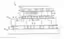
FIG. 1 of the accompanying drawings illustrates an interposer substrate 10 which has been constructed according to a method of an embodiment of the invention. The interposer substrate 10 includes a base structure 12, conductive vias 14, a capacitor structure 16 having a high k-value dielectric material, a low k-value dielectric material 18, and contact pads 20.
The base structure 12 is initially made from a green, unsintered material. The green material is package in the shape of the base structure 12 and via openings 22 are then punched through the green material. Handling, packaging and punching of green material is known in the art. An advantage of punching holes in a green material is that the green material is not as brittle as other substrates such as silicon substrates. The green material is subsequently sintered so that the green material becomes a sintered ceramic material and the base structure 12 becomes a sintered ceramic base structure 12. The sintered ceramic base structure 12 then has the via openings 22. The via openings 22 include a power via opening 22P, a ground via opening 22G, and signal via openings 22S. Each one of the via openings 22 extends from a lower surface through an upper surface of the horizontal sintered ceramic base structure 12.
The low k-value dielectric material 18 is then formed over the entire upper surface of the sintered ceramic base structure 12. The low k-value dielectric material 18 thus covers the power, ground and signal via openings 22P, 22G and 22S. The low k-value dielectric material 18 is typically made of silicon dioxide, which has a dielectric constant of between three and four.
The low k-value dielectric material 18 is subsequently patterned. The low k-value dielectric material 18 may for example be patterned by first covering a portion thereof and then burning exposed portions away. The portions that are burned away (or etched) are portions thereof located over the power and ground via openings 22P and 22G. Openings are also burned (or etched) in the low k-value dielectric material 18 so that the signal via openings 22S extend vertically through the low k-value dielectric material 18.
The capacitor structure 16 is then formed on the sintered ceramic base structure 12 where the low k-value dielectric material 18 has been burned away (or etched). That is, the capacitor structure 16 is formed on an area of the upper surface of the sintered ceramic base structure 12 that has the power and ground via openings 22P and 22G. The capacitor structure 16 includes power and ground planes 24 and 26 and a dielectric layer 28. The power and ground planes are typically made of copper or platinum. The dielectric layer 28 is made of a high k-value dielectric material which may have a dielectric constant of between 300 and 900, although the dielectric constant may be as high as 3000. An insulating layer 30 is formed on top of the ground plane 26 in order to add a second capacitance and is made of the same material as the dielectric layer 28. More layers could be added for extra capacitance. The layers and planes 24, 26, 28 and 30 are all patterned so that the power and ground via openings 22P and 22G extend vertically through the entire capacitor structure 16. The manufacture of thin film capacitor structures such as the capacitor structure 16 is known in the art.
The via openings 22 are all subsequently filled with the conductive vias 14. The conductive vias 14 are typically formed from a conductive metal such as copper, silver or an alloy of tungsten and molybdenum. The conductive vias may for example be sputter-deposited, plated or printed, within the via openings 22. The conductive vias 14 include power, ground and signal conductive vias 14P, 14G and 14S in the power, ground and signal via openings 22P, 22G and 22S, respectively. The power conductive via 14P is in contact with the power plane 24 and is not connected to the ground plane 26. The ground conductive via 14G is in contact with the ground plane 26 and is not connected to the power plane 24. Each signal conductive via 14S is electrically disconnected from all other conductive vias 14P, 14G and 14S.
The contact pads 20 are then formed on the capacitor structure 16 and the low k-value dielectric material 18. Each contact pad 20 is located on and electrically connected to a respective one of the conductive vias 14.
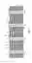
FIG. 2 illustrates the interposer substrate 10 within an integrated circuit package 34 according to an embodiment of the invention. The integrated circuit package 34 further includes a carrier substrate 36, a package substrate 38, a die 40 and respective sets of conductive interconnection members 42, 44, and 46.
The package substrate 38 has a base structure 48, a plurality of conductive lines 50 within the base structure 48, a plurality of contact pads 52 on a lower surface of base structure 48, and a plurality of contact pads 54 on an upper surface of base structure 48. The base structure 48 is made of a low k-value dielectric material. In the given example, each one of the conductive lines 50 interconnects a respective one of the contact pads 52 with a respective one of the contact pads 54. Some of the conductive lines 50 have two vertical vias 56 and 58 that are interconnected by a horizontal line 60. The inclusion of the horizontal line 60 allows for the contact pads 54 to be offset with respect to the contact pads 52. The conductive lines 50 thus allow for an x-y transformation from the contact pads 52 to the contact pads 54.
As illustrated, the interposer substrate 10 further has a plurality of contact pads 62 on a lower surface of a sintered ceramic base structure 12. There is no x-y transformation from the contact pads 62 at the lower side of the interposer substrate 10 to the contact pads 20 at the upper side of the interposer substrate 10. Each one of the contact pads 62 matches up with a respective one of the contact pads 54 and a respective one of the conductive interconnection members 44 interconnects a respective one of the contact pads 62 with a respective one of the contact pads 54.
The die 40 has an integrated circuit formed in a lower surface thereof. A plurality of contact pads 64 are formed on a lower surface of the die 40 and are electrically connected to the integrated circuit. Each one of the contact pads 64 matches up with a respective one of the contact pads 20 and is connected thereto by a respective one of the conductive interconnection members 46. It can thus be seen that there is no x-y transformation from the contact pads 64 to the contact pads 54 and that there is an x-y transformation from the contact pads 54 to the contact pads 52.
The carrier substrate 36 has a respective base structure 66 and a plurality of contact pads 68 formed on an upper surface of the base structure 66. Each one of the contact pads 52 is aligned with a respective one of the contact pads 68 and is connected thereto by a respective one of the conductive interconnection members 42.
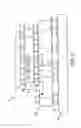
FIG. 3 illustrates a package substrate 138 which is manufactured according to a method of another embodiment of the invention. The package substrate 138 includes a sintered ceramic base structure 112, a capacitor structure 116, a low k-value dielectric material 118, and contact pads 120 that are the same as the sintered ceramic base structure 12, capacitor structure 16, and contact pads 20 of the interposer substrate 10 of FIG. 1. The package substrate 138 differs from the interposer substrate 10 in that conductive lines 150 are provided instead of the conductive vias 14.
Each one of the conductive lines includes two vertical vias 156 and 158 and a horizontal line 160 interconnecting the vertical vias 156 and 158. The sintered ceramic base structure 112 is formed in stages so that the horizontal line 160 is buried below an upper surface of the sintered ceramic base structure 112. The horizontal line 160 allows for the vertical vias 156 and 158 to be horizontally offset with respect to one another. The horizontal lines 160 thus allow for x-y transformation on the vertical vias 156 to the vertical vias 158.
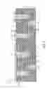
FIG. 4 illustrates an integrated circuit package which includes the package substrate 138, a carrier substrate 136 and a die 140. The die 140 and carrier substrate 136 are the same as the die 40 and carrier substrate 36 of the integrated circuit package 34 of FIG. 2. The integrated circuit package 134 differs from the integrated circuit package 34 in that there is no intermediate interposer substrate between the die 140 and the package substrate 138. In the integrated circuit package 34 of FIG. 2, the interposer substrate 10 provides a capacitor structure 16 close to the die 40 and the package substrate 38 provides an x-y transformation. In the integrated circuit package 134 of FIG. 4, by contrast, the package substrate 138 provides a capacitor structure 116 close to the die 140 and provides x-y transformation.
While certain exemplary embodiments have been described and shown in the accompanying drawings, it is to be understood that such embodiments are merely illustrative and not restrictive of the current invention, and that this invention is not restricted to the specific constructions and arrangements shown and described since modifications may occur to those ordinarily skilled in the art.
Claims
What is claimed:1. A method of constructing at least a portion of an integrated circuit package, comprising:
forming a base structure, of a green material, having a plurality of via openings therein;
sintering the green material so that the green material becomes a sintered ceramic material and the base structure becomes a sintered ceramic base structure having the via openings;
forming a conductive via in each via opening of the sintered ceramic base structure, the conductive vias including at least power and ground vias; and
forming a capacitor structure on the sintered ceramic base structure, the capacitor structure including conductive power and ground planes and a dielectric layer between the power and ground planes, the power and ground planes being electrically connected to at least one of the power vias and one of the ground vias, respectively.
2. The method of claim 1 wherein the vias include signal vias, each signal via being electrically disconnected from both the power and ground planes.
3. The method of claim 2 wherein the dielectric layer of the capacitor structure is made of a dielectric material with a high k-value, the substrate having first and second portions, the first portion having the high k-value dielectric material and the second portion not having the high k-value dielectric material, the signal vias being formed in the second portion.
4. The method of claim 1 further comprising:
mounting the base structure with the capacitor structure thereon, jointly forming an interposer substrate, on the package substrate; and
mounting a die having a microelectronic circuit formed therein to the interposer substrate
5. The method of claim 4 further comprising:
forming a plurality of conductive members on the package substrate for interconnection with a carrier substrate
Images & Drawings included:
Sources:
- United States Patent and Trademark Office - verify current appl. status at the USPTO↗
Similar patent applications:
Recent applications in this class:
- » 20250071902 2025-02-27
PRINTED CIRCUIT BOARD - » 20250040051 2025-01-30
CAPACITIVE ELEMENT, CIRCUIT CARRIER HAVING THE SAME AND FABRICATION METHOD THEREOF - » 20250008659 2025-01-02
PRINTED CIRCUIT BOARD - » 20240431029 2024-12-26
INTEGRATED ASSEMBLY AND INTEGRATED POWER CONVERTER MODULE - » 20240224426 2024-07-04
WIRING SUBSTRATE - » 20230371181 2023-11-16
CIRCUIT BOARD SYSTEMS AND METHODS - » 20230319997 2023-10-05
CAPACITOR IN A SUBSTRATE VIA - » 20220369461 2022-11-17
Automatic trimming of a PCB-based LC circuit - » 20220053644 2022-02-17
Passive device packaging structure embedded in glass medium and method for manufacturing the same - » 20210219430 2021-07-15
Electronic component and its manufacturing method
Recent applications for this Assignee:
- » 20250294866 2025-09-18
GATE CUT CONFINED WITHIN GATE TRENCH - » 20250294846 2025-09-18
BACKSIDE CROSS-COUPLE INTERCONNECTS - » 20250294835 2025-09-18
ELONGATED VERTICAL STRUCTURES OF CHANNEL MATERIALS - » 20250294827 2025-09-18
CO-INTEGRATION OF GATE-ALL-AROUND DEVICES WITH DIFFERENT NUMBERS OF NANORIBBONS - » 20250294818 2025-09-18
TRANSISTOR DESIGNS FOR FLOATING BODY MEMORY - » 20250294781 2025-09-18
MAGNETIC CORE INDUCTORS ON PACKAGE SUBSTRATES - » 20250294777 2025-09-18
INTEGRATED CIRCUIT DEVICE WITH MEMORY ARRAY AND SHARED GAIN ELEMENT - » 20250293985 2025-09-18
RECEIVER-BASED PRECISION CONGESTION CONTROL - » 20250293860 2025-09-18
PRESERVATION OF CONFIDENTIALITY AND INTEGRITY OF MODELS DURING EXECUTION - » 20250293706 2025-09-18
LOW-RANK DECOMPOSITION-BASED HARDWARE COMPRESSION OF MATRICES AND TENSORS