Light emitting diode
US20070152309A1
2007-07-05
11/319,649
2005-12-29
Abstract:
A light emitting diode comprises: at least two electrodes; a first encapsulant layer; at least a chip; and a second encapsulant layer. The electrodes are fixed by the first encapsulant layer. The chip is electrically connected to the electrodes. The chip and the electrodes are covered with the second encapsulant layer. As a result, the substrate-free, super-thin light emitting diode is completed.
Interested in similar patents?
Get notified when new applications in this technology area are published.
Classification:
H01L33/486 » CPC main
Semiconductor devices with at least one potential-jump barrier or surface barrier specially adapted for light emission; Processes or apparatus specially adapted for the manufacture or treatment thereof or of parts thereof; Details thereof characterised by the semiconductor body packages; Containers adapted for surface mounting
H01L24/73 » CPC further
Arrangements for connecting or disconnecting semiconductor or solid-state bodies; Methods or apparatus related thereto Means for bonding being of different types provided for in two or more of groups , , , , , , ,
H01L33/62 » CPC further
Semiconductor devices with at least one potential-jump barrier or surface barrier specially adapted for light emission; Processes or apparatus specially adapted for the manufacture or treatment thereof or of parts thereof; Details thereof characterised by the semiconductor body packages Arrangements for conducting electric current to or from the semiconductor body, e.g. lead-frames, wire-bonds or solder balls
H01L2224/16 » CPC further
Indexing scheme for arrangements for connecting or disconnecting semiconductor or solid-state bodies and methods related thereto as covered by; Means for bonding being attached to, or being formed on, the surface to be connected, e.g. chip-to-package, die-attach, "first-level" interconnects; Manufacturing methods related thereto; Bump connectors; Manufacturing methods related thereto; Structure, shape, material or disposition of the bump connectors after the connecting process of an individual bump connector
H01L2924/01005 » CPC further
Indexing scheme for arrangements or methods for connecting or disconnecting semiconductor or solid-state bodies as covered by; Chemical elements Boron [B]
H01L2924/01006 » CPC further
Indexing scheme for arrangements or methods for connecting or disconnecting semiconductor or solid-state bodies as covered by; Chemical elements Carbon [C]
H01L2924/01033 » CPC further
Indexing scheme for arrangements or methods for connecting or disconnecting semiconductor or solid-state bodies as covered by; Chemical elements Arsenic [As]
H01L2924/00014 » CPC further
Indexing scheme for arrangements or methods for connecting or disconnecting semiconductor or solid-state bodies as covered by; Technical content checked by a classifier the subject-matter covered by the group, the symbol of which is combined with the symbol of this group, being disclosed without further technical details
H01L2924/12041 » CPC further
Indexing scheme for arrangements or methods for connecting or disconnecting semiconductor or solid-state bodies as covered by; Details of semiconductor or other solid state devices to be connected; Device type; Passive devices, e.g. 2 terminal devices; Optical Diode LED
H01L2924/00 » CPC further
Indexing scheme for arrangements or methods for connecting or disconnecting semiconductor or solid-state bodies as covered by
H01L23/495 IPC
Details of semiconductor or other solid state devices; Arrangements for conducting electric current to or from the solid state body in operation, e.g. leads, terminal arrangements ; Selection of materials therefor consisting of soldered constructions Lead-frames or other flat leads
Description
FIELD OF THE INVENTIONThe present invention relates to a light emitting diode (LED) or the like, and more particularly to a substrate-free light emitting diode with significantly reduced thickness.
BACKGROUND OF THE INVENTIONLight emitting diode is a kind of small-sized, high-efficient, solid-state light source. The light emitting diode is a semiconductor device so it has long lifetime and high stability. The light emitting diode is suitable to be various light sources, e.g. monitors' light sources, backlight plates' light sources, traffic lights, emergency guiding lights, lighting, etc.
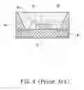
Referring to FIG. 4, a conventional light emitting diode, which is formed by SMD (surface mount device) technology, is shown. The conventional light emitting diode includes a substrate A on which electrodes B and a trench A1 are formed. A chip C is coupled to the substrate A in the trench A1, and the chip C is further connected to the electrodes B by bonding wires D. Thereafter, the trench A1 is filled with encapsulant E so as to integrate several above-mentioned devices into a unity.
Although the conventional light emitting diode is convenient in use and its thickness can be reduced to 0.3 mm by modern packaging technology, it still has a certain thickness. For the portable electronic machines, their components' thickness should be further reduced to bring about light, thin, short, and small electronic products.
In view of the foregoing description, the present inventor makes diligent studies in providing consumers with a substrate-free light emitting diode having significantly reduced thickness according to the motive of the present invention.
SUMMARY OF THE INVENTIONIt is a main object of the present invention to provide a substrate-free light emitting diode with significantly reduced thickness.
In order to achieve this object, a light emitting diode of the present invention comprises: at least two electrodes; a first encapsulant layer; at least a chip; and a second encapsulant layer. The electrodes are fixed by the first encapsulant layer. The chip is electrically connected to the electrodes. The chip and the electrodes are covered with the second encapsulant layer. As a result, the substrate-free, super-thin light emitting diode is completed.
The aforementioned objects and advantages of the present invention will be readily clarified in the description of the preferred embodiments and the enclosed drawings of the present invention.
BRIEF DESCRIPTION OF THE DRAWINGSFIG. 1 is an assembled sectional view showing a first preferred embodiment of the present invention.
FIG. 2 is an assembled sectional view showing a second preferred embodiment of the present invention.
FIG. 3 is an assembled sectional view showing a third preferred embodiment of the present invention.
FIG. 4 is an assembled sectional view showing a conventional structure.
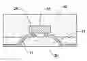
DETAILED DESCRIPTION OF THE PREFERRED EMBODIMENTReferring to FIG. 1, a first preferred embodiment of the present invention is shown. Two electrodes 10, 11 are provided, wherein these two electrodes 10, 11 are partially covered with a first encapsulant layer 20. The first encapsulant layer 20 is, for example, PI or SU8. A chip 30 is flip-chip bonded to these two electrodes 10, 11 on exposed portions where they are not covered with the first encapsulant layer 20 by tin solders 25. Thereafter, the exposed portions of these two electrodes 10, 11 and the chip 30 are totally covered with a second encapsulant layer 40 such that a substrate-free light emitting diode is completed.
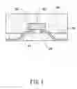
As shown in FIG. 2, these two electrodes 10, 11 are fixed by the first encapsulant layer 20, and then the chip 30 is mounted on the top of the first encapsulant layer 20. Thereafter, the chip 30 is electrically connected to these two electrodes 10, 11 by two bonding wires 26, 27. Finally, the chip 30 and these two bonding wires 26, 27 are covered with the second encapsulant layer 40 such that a substrate-free, super-thin light emitting diode is completed.
As shown in FIG. 3, these two electrodes 10, 11 have unequal lengths. Similarly, these two electrodes 10, 11 are fixed by the first encapsulant layer 20, and the chip 30 is flip-chip bonded to the top of the electrode 10 by the tin solder 25. Besides, the chip 30 is electrically connected to the electrode 11 by the bonding wire 26. Thereafter, the chip 30 and the bonding wire 26 are covered with the second encapsulant layer 40 such that a substrate-free, super-thin light emitting diode is completed.
Moreover, the first encapsulant layer 20 shown in FIG. 1, FIG. 2, and FIG. 3 is, for example, poly methylmethacrylate (PMMA), poly dimethylsioxane (PDMS), poly carbonate (PC), polyimide (PI), epoxy resin (SU-8), spin on glass (SOG), silicon gel, or resin. Besides, the second encapsulant layer 40 is, for example, silicon gel, resin, a mixture of silicon gel and fluorescent powders, or a mixture of resin and fluorescent powders.
In summary, the light emitting diode of the present invention is substrate-free and has significantly reduced thickness. Accordingly, the present invention satisfies patentability and is submitted for a patent.
While the preferred embodiment of the invention has been set forth for the purpose of disclosure, modifications of the disclosed embodiment of the invention as well as other embodiments thereof may occur to those skilled in the art. Accordingly, the appended claims are intended to cover all embodiments, which do not depart from the spirit and scope of the invention.
Claims
What the invention claimed is:1. A light emitting diode comprising:
at least two electrodes;
a first encapsulant layer for fixing the electrodes;
at least a chip electrically connected to the electrodes; and
a second encapsulant layer for covering the chip and the electrodes such that the substrate-free, super-thin light emitting diode is completed.
2. The light emitting diode of claim 1, wherein the chip is electrically connected to the electrodes by a wire-bonding method.
3. The light emitting diode of claim 1, wherein the chip is electrically connected to the electrodes by a flip-chip mounting method.
4. The light emitting diode of claim 1, wherein the chip is electrically connected to the electrodes by a wire-bonding method and a flip-chip mounting method, respectively.
5. The light emitting diode of claim 1, wherein the first encapsulant layer is poly methylmethacrylate (PMMA), poly dimethylsioxane (PDMS), poly carbonate (PC), polyimide (PI), epoxy resin (SU-8), spin on glass (SOG), silicon gel, or resin.
6. The light emitting diode of claim 1, wherein the second encapsulant layer is silicon gel.
7. The light emitting diode of claim 6, wherein the second encapsulant layer is doped with fluorescent powders.
8. The light emitting diode of claim 1, wherein the second encapsulant layer is resin.
9. The light emitting diode of claim 8, wherein the second encapsulant layer is doped with fluorescent powders.
Images & Drawings included:
Sources:
- United States Patent and Trademark Office - verify current appl. status at the USPTO↗
Similar patent applications:
- » 20080210957
Light emitting diode, method for manufacturing light emitting diode, integrated light emitting diode, method for manufacturing integrated light emitting diode, light emitting diode backlight, light emitting diode illumination device, light emitting diode display, electronic apparatus, electronic device, and method for manufacturing electronic device - » 20060278886
Light emitting diode, method of manufacturing light emitting diode, light emitting diode backlight, light emitting diode illuminating device, light emitting diode display, and electronic apparatus - » 20100308349
LIGHT-EMITTING DIODE, METHOD FOR MAKING LIGHT-EMITTING DIODE, INTEGRATED LIGHT-EMITTING DIODE AND METHOD FOR MAKING INTEGRATED LIGHT-EMITTING DIODE, METHOD FOR GROWING A NITRIDE-BASED III-V GROUP COMPOUND SEMICONDUCTOR, LIGHT SOURCE CELL UNIT, LIGHT-EMITTING DIODE BACKLIGHT, AND LIGHT-EMITTING DIODE DISPLAY AND ELECTRONIC DEVICE - » 20080121903
METHOD FOR MANUFACTURING LIGHT-EMITTING DIODE, LIGHT-EMITTING DIODE, LIGHTSOURCE CELL UNIT, LIGHT-EMITTING DIODE BACKLIGHT, LIGHT-EMITTING DIODE ILLUMINATING DEVICE, LIGHT-EMITTING DIODE DISPLAY, AND ELECTRONIC APPARATUS - » 20190035979
Light emitting diode, method for manufacturing light emitting diode, light emitting diode display device, and method for manufacturing light emitting diode display device - » 20060258027
Light-emitting diode, method for making light-emitting diode, integrated light-emitting diode and method for making integrated light-emitting diode, method for growing a nitride-based III-V group compound semiconductor, light source cell unit, light-emitting diode - » 20070246730
Light emitting diode and light emitting diode device including the light emitting diode element and method for manufacturing the light emitting diode - » 20070241361
Light emitting diode and light emitting diode device including the light emitting diode element and method for manufacturing the light emitting diode - » 20200100334
Light emitting diode module, light emitting diode driver, and light emitting diode lighting apparatus - » 20160099385
Method for manufacturing vertical type light emitting diode, vertical type light emitting diode, method for manufacturing ultraviolet ray light emitting diode, and ultraviolet ray light emitting diode
Recent applications in this class:
- » 20250063861 2025-02-20
LIGHT EMITTING MODULE HAVING LIGHT EMITTING DEVICE AND DISPLAY APPARATUS HAVING SAME - » 20250048800 2025-02-06
BASE MEMBER FOR LIGHT EMITTING DEVICE - » 20250040313 2025-01-30
LIGHT EMITTING DEVICE AND LIGHT EMITTING MODULE INCLUDING THE SAME - » 20250040311 2025-01-30
LED CIRCUIT BOARD AND LIGHT EMITTING MODULE - » 20250015235 2025-01-09
METHOD FOR ATTACHING MICRO LEDS TO DISPLAY BY USING FLUID AS SOFT LANDING MEDIUM FOR MICRO LEDS - » 20250006869 2025-01-02
LIGHT EMITTING DIODE PACKAGE AND METHOD OF MANUFACTURING THE SAME - » 20240429350 2024-12-26
OPTOELECTRONIC COMPONENT - » 20240413270 2024-12-12
SEMICONDUCTOR LIGHT-EMITTING APPARATUS - » 20240363809 2024-10-31
Display Device - » 20240363808 2024-10-31
OPTOELECTRONIC SEMICONDUCTOR COMPONENT AND PRODUCTION METHOD