Solder wall structure in flip-chip technologies
US20070176288A1
2007-08-02
11/275,867
2006-02-01
✅ Patent granted
US 7,547,576 B2
2009-06-16
-
-
N Drew Richards | Christy L Novacek
2026-12-26
Abstract:
A structure and method for forming the same. The semiconductor structure includes a first semiconductor chip and N solder bumps in direct physical contact with the first semiconductor chip, wherein N is a positive integer. The semiconductor structure also includes a first solder wall on a perimeter of the first semiconductor chip such that the first solder wall forms a closed loop surrounding the N solder bumps.
Inventors:
- Jeffrey Peter Gambino 68 🇺🇸 Westford, VT, United States
- Timothy Harrison Daubenspeck 30 🇺🇸 Colchester, VT, United States
- Wolfgang Sauter 101 🇺🇸 Richmond, VT, United States
- Timothy H. Daubenspeck 123 🇺🇸 Colchester, VT, United States
- Christopher David Muzzy 24 🇺🇸 Burlington, VT, United States
Assignee:
- INTERNATIONAL BUSINESS MACHINES CORPORATION 136,239 🇺🇸 ARMONK, NY, United States
Interested in similar patents?
Get notified when new applications in this technology area are published.
Classification:
H01L24/13 » CPC main
Arrangements for connecting or disconnecting semiconductor or solid-state bodies; Methods or apparatus related thereto; Means for bonding being attached to, or being formed on, the surface to be connected, e.g. chip-to-package, die-attach, "first-level" interconnects; Manufacturing methods related thereto; Bump connectors ; Manufacturing methods related thereto; Structure, shape, material or disposition of the bump connectors prior to the connecting process of an individual bump connector
H01L23/562 » CPC further
Details of semiconductor or other solid state devices Protection against mechanical damage
H01L24/05 » CPC further
Arrangements for connecting or disconnecting semiconductor or solid-state bodies; Methods or apparatus related thereto; Means for bonding being attached to, or being formed on, the surface to be connected, e.g. chip-to-package, die-attach, "first-level" interconnects; Manufacturing methods related thereto; Bonding areas ; Manufacturing methods related thereto; Structure, shape, material or disposition of the bonding areas prior to the connecting process of an individual bonding area
H01L24/11 » CPC further
Arrangements for connecting or disconnecting semiconductor or solid-state bodies; Methods or apparatus related thereto; Means for bonding being attached to, or being formed on, the surface to be connected, e.g. chip-to-package, die-attach, "first-level" interconnects; Manufacturing methods related thereto; Bump connectors ; Manufacturing methods related thereto Manufacturing methods
H01L24/29 » CPC further
Arrangements for connecting or disconnecting semiconductor or solid-state bodies; Methods or apparatus related thereto; Means for bonding being attached to, or being formed on, the surface to be connected, e.g. chip-to-package, die-attach, "first-level" interconnects; Manufacturing methods related thereto; Layer connectors, e.g. plate connectors, solder or adhesive layers; Manufacturing methods related thereto; Structure, shape, material or disposition of the layer connectors prior to the connecting process of an individual layer connector
H01L24/73 » CPC further
Arrangements for connecting or disconnecting semiconductor or solid-state bodies; Methods or apparatus related thereto Means for bonding being of different types provided for in two or more of groups , , , , , , ,
H01L2224/05001 » CPC further
Indexing scheme for arrangements for connecting or disconnecting semiconductor or solid-state bodies and methods related thereto as covered by; Means for bonding being attached to, or being formed on, the surface to be connected, e.g. chip-to-package, die-attach, "first-level" interconnects; Manufacturing methods related thereto; Bonding areas; Manufacturing methods related thereto; Structure, shape, material or disposition of the bonding areas prior to the connecting process of an individual bonding area Internal layers
H01L2224/16 » CPC further
Indexing scheme for arrangements for connecting or disconnecting semiconductor or solid-state bodies and methods related thereto as covered by; Means for bonding being attached to, or being formed on, the surface to be connected, e.g. chip-to-package, die-attach, "first-level" interconnects; Manufacturing methods related thereto; Bump connectors; Manufacturing methods related thereto; Structure, shape, material or disposition of the bump connectors after the connecting process of an individual bump connector
H01L2924/01005 » CPC further
Indexing scheme for arrangements or methods for connecting or disconnecting semiconductor or solid-state bodies as covered by; Chemical elements Boron [B]
H01L2924/01006 » CPC further
Indexing scheme for arrangements or methods for connecting or disconnecting semiconductor or solid-state bodies as covered by; Chemical elements Carbon [C]
H01L2924/01013 » CPC further
Indexing scheme for arrangements or methods for connecting or disconnecting semiconductor or solid-state bodies as covered by; Chemical elements Aluminum [Al]
H01L2924/01029 » CPC further
Indexing scheme for arrangements or methods for connecting or disconnecting semiconductor or solid-state bodies as covered by; Chemical elements Copper [Cu]
H01L2924/01078 » CPC further
Indexing scheme for arrangements or methods for connecting or disconnecting semiconductor or solid-state bodies as covered by; Chemical elements Platinum [Pt]
H01L2924/014 » CPC further
Indexing scheme for arrangements or methods for connecting or disconnecting semiconductor or solid-state bodies as covered by; Alloys Solder alloys
H01L2924/01082 » CPC further
Indexing scheme for arrangements or methods for connecting or disconnecting semiconductor or solid-state bodies as covered by; Chemical elements Lead [Pb]
H01L2924/0001 » CPC further
Indexing scheme for arrangements or methods for connecting or disconnecting semiconductor or solid-state bodies as covered by Technical content checked by a classifier
H01L2224/13099 » CPC further
Indexing scheme for arrangements for connecting or disconnecting semiconductor or solid-state bodies and methods related thereto as covered by; Means for bonding being attached to, or being formed on, the surface to be connected, e.g. chip-to-package, die-attach, "first-level" interconnects; Manufacturing methods related thereto; Bump connectors; Manufacturing methods related thereto; Structure, shape, material or disposition of the bump connectors prior to the connecting process of an individual bump connector; Core members of the bump connector Material
H01L2924/15787 » CPC further
Indexing scheme for arrangements or methods for connecting or disconnecting semiconductor or solid-state bodies as covered by; Details of package parts other than the semiconductor or other solid state devices to be connected; Die mounting substrate; Material with a principal constituent of the material being a non metallic, non metalloid inorganic material Ceramics, e.g. crystalline carbides, nitrides or oxides
H01L2924/00 » CPC further
Indexing scheme for arrangements or methods for connecting or disconnecting semiconductor or solid-state bodies as covered by
H01L2924/00014 » CPC further
Indexing scheme for arrangements or methods for connecting or disconnecting semiconductor or solid-state bodies as covered by; Technical content checked by a classifier the subject-matter covered by the group, the symbol of which is combined with the symbol of this group, being disclosed without further technical details
H01L23/48 IPC
Details of semiconductor or other solid state devices Arrangements for conducting electric current to or from the solid state body in operation, e.g. leads, terminal arrangements ; Selection of materials therefor
H01L21/00 IPC
Processes or apparatus adapted for the manufacture or treatment of semiconductor or solid state devices or of parts thereof
Description
BACKGROUND OF THE INVENTION1. Technical Field
The present invention relates to flip-chip technologies, and more specifically, to a solder wall structure in flip-chip technologies.
2. Related Art
In typical flip-chip technologies, solder bumps are formed on top of a chip to help bond the chip to a ceramic substrate. These solder bumps may be corroded by carbon dioxide and water vapor of the surrounding ambient environment. Therefore, there is a need for a structure (and a method for forming the same), in which the solder bumps are not corroded by carbon dioxide and water vapor of the surrounding ambient.
SUMMARY OF THE INVENTIONThe present invention provides a semiconductor structure, comprising (a) a first semiconductor chip; (b) N solder bumps in direct physical contact with the first semiconductor chip, wherein N is a positive integer; and (c) a first solder wall on a perimeter of the first semiconductor chip such that the first solder wall forms a closed loop surrounding the N solder bumps.
The present invention also provides a semiconductor fabrication method, comprising providing a first semiconductor chip; forming N solder bumps in direct physical contact with the first semiconductor chip, wherein N is a positive integer; and forming a first solder wall on a perimeter of the first semiconductor chip such that the first solder wall forms a closed loop surrounding the N solder bumps.
The present invention also provides a semiconductor structure, comprising (a) a first semiconductor chip comprising a crack stop on a perimeter of the first semiconductor chip; (b) N solder bumps in direct physical contact with the first semiconductor chip, wherein N is a positive integer; (c) a first solder wall on a perimeter of the first semiconductor chip such that the first solder wall forms a closed loop surrounding the N solder bumps, and such that the first solder wall is overlapping the crack stop; and (d) a module substrate coupled to the first solder wall and the N solder bumps
Therefore, there is a need for a structure (and a method for forming the same), in which the solder bumps are not corroded by carbon dioxide and water vapor of the surrounding ambient.
BRIEF DESCRIPTION OF THE DRAWINGSFIGS. 1A-1G illustrate a fabrication method for forming a semiconductor structure, in accordance with embodiments of the present invention.
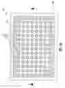
FIG. 1Fi shows a top-down view of the semiconductor structure of FIG. 1F, in accordance with embodiments of the present invention.
FIG. 1Gi shows a top-down view of a semiconductor chip after it is cut from the semiconductor structure of FIG. 1G, in accordance with embodiments of the present invention.
FIG. 2 illustrates a fabrication method for forming a module, in accordance with embodiments of the present invention.
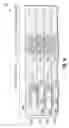
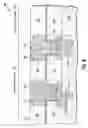
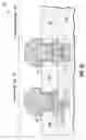
DETAILED DESCRIPTION OF THE INVENTIONFIGS. 1A-1G illustrate a fabrication method for forming a semiconductor structure 100, in accordance with embodiments of the present invention. More specifically, with reference to FIG. 1A, in one embodiment, the fabrication of the semiconductor structure 100 starts with a semiconductor chip 102 and a dicing channel region 104. The semiconductor chip 102 comprises multiple interconnect layers 106a, 106b, 106c, and 106d. There may be additional device layers in a silicon substrate of the semiconductor chip 102 beneath and coupled to the interconnect layer 106d, but these additional device layers and the silicon substrate are not shown for simplicity. In the embodiment described above, there are only four interconnect layers 106a, 106b, 106c, and 106d. In general, the semiconductor chip 102 can have N interconnect layers, wherein N is a positive integer.
In one embodiment, the top interconnect layer 106a of the semiconductor chip 102 includes (i) a dielectric layer 110a, (ii) an electrically conducting line 120a (comprising copper (Cu) in one embodiment) embedded in the dielectric layer 110a, and (iii) a metal region 122a (comprising Cu in one embodiment) embedded in the dielectric layer 110a. Similarly, the interconnect layers 106b, 106c, and 106d comprise dielectric layers 110b, 110c, and 110d, electrically conducting lines 120b, 120c, and 120d (comprising Cu in one embodiment), and metal regions 122b, 122c, and 122d (comprising Cu in one embodiment), respectively. In one embodiment, the metal regions 122a, 122b, 122c, and 122d run on a perimeter of the semiconductor chip 102 and form a crack stop 122 surrounding the semiconductor chip 102. In one embodiment, the crack stop 122 is to prevent cracking from propagating from the dicing channel region 104 to the semiconductor chip 102 during a chip dicing process. It should be noted that from FIG. 1B to FIG. 1G, a bottom part of the structure 100, which comprises the interconnect layers 106b, 106c, and 106d, is omitted for simplicity, the only top interconnect layer 106a is shown.
Next, with reference to FIG. 1B, in one embodiment, portions of the dielectric layer 110a are removed so as to create a hole 124 and a trench 126 such that top surfaces 125 and 127 of the Cu line 120a and the crack stop 122, respectively, are exposed to the surrounding ambient. In one embodiment, the trench 126 runs along the crack stop 122 of the chip 102.
Next, in one embodiment, a bond pad 130 (comprising aluminum (Al) in one embodiment) is formed on top of the Cu line 120a and the dielectric layer 110a such that the Al bond pad 130 is electrically coupled to the Cu line 120a. In one embodiment, a wall base 132 (comprising Al in one embodiment) is formed on top of the crack stop 122 and the dielectric layer 110a such that the Al wall base 132 is in direct physical contact with the crack stop 122. Illustratively, the Al bond pad 130 and the Al wall base 132 can be simultaneously formed by (a) forming an Al layer (not shown) on the entire structure 100, and then (b) directionally and selectively etching back the Al layer stopping at the dielectric layer 110a. The directional and selective etching in step (b) may be performed using a traditional lithographic and etching process such that what remains of the Al layer after the etching are the Al bond pad 130 and the Al wall base 132 (as shown in FIG. 1B). In one embodiment, the Al wall base 132 runs along the crack stop 122 of the chip 102 (i.e. the Al wall base 132 runs on the perimeter of the semiconductor chip 102).
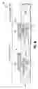
Next, with reference to FIG. 1C, in one embodiment, a patterned support/interface layer 140 (comprising polyimide in one embodiment) is formed on top of the entire structure 100 of FIG. 1B. In one embodiment, the patterned support/interface layer 140 comprises a hole 142 and a trench 146 such that (i) a top surface 144 of the Al bond pad 130 is exposed to the surrounding ambient environment via the hole 142 and (ii) a top surface 148 of the Al wall base 132 is exposed to the surrounding ambient environment via the trench 146. In one embodiment, the trench 146 runs along the Al wall base 132 of the chip 102 (i.e. the trench 146 runs on the perimeter of the semiconductor chip 102).
In one embodiment, the patterned support/interface layer 140 is formed using a photosensitive method. More specifically, the patterned support/interface layer 140 is formed by (i) spin-applying a polyimide film (not shown) on the structure 100 of FIG. 1B, (ii) then curing the polyimide film at a high temperature, (iii) then exposing the polyimide film to light through a mask (not shown) in a photo stepper lithographic tool (not shown), (iv) and then developing the polyimide film so as to form the patterned support/interface layer 140. It should be noted that polyimide is a photosensitive polymer. In general, other photosensitive polymers may be used instead of polyimide.
Next, with reference to FIG. 1D, in one embodiment, a bump limiting metallurgy (BLM) film 150 is formed on top of the entire structure 100 of FIG. 1C by, illustratively, sputter deposition or plating or a combination of sputter deposition and plating.
Next, with reference to FIG. 1E, in one embodiment, a patterned photo-resist layer 160 is formed on top of the BLM film 150. In one embodiment, the patterned photo-resist layer 160 is formed by using a conventional lithographic process. In one embodiment, the patterned photo-resist layer 160 comprises (i) a hole 162 aligned with the hole 142 and (ii) a trench 166 aligned with the trench 146 such that top surfaces 164 and 168 of the BLM film 150 are exposed to the surrounding ambient environment via the hole 162 and the trench 166, respectively. It should be noted that the holes 142 and 162 can be collectively referred to as a hole 142,162. Similarly, the trenches 146 and 166 can be collectively referred to as a trench 146,166. In one embodiment, the trench 146,166 runs on the perimeter of the semiconductor chip 102.
Next, in one embodiment, a solder bump 170 (comprising a mixture of lead (Pb) and tin (Sn) in one embodiment) and a solder wall 172 (comprising a mixture of Pb and Sn in one embodiment) are simultaneously formed in the hole 142,162 and the trench 146,166, respectively, by, illustratively, electroplating. More specifically, in one embodiment, the structure 100 is submerged in a solution (not shown) containing tin and lead ions. The BLM film 150 is electrically coupled to the cathode of an external dc (direct current) power supply (not shown), while the solution is electrically coupled to the anode of the dc supply. Under the electric field created in the solution by the dc power supply, tin and lead ions in the solution arrive at the exposed surfaces 164 and 168 of the BLM film 150 and deposit there forming the solder bump 170 and the solder wall 172, respectively, as shown in FIG. 1E. In one embodiment, the solder wall 172 runs along the trench 146,166 (i.e. the solder wall 172 runs on the perimeter of the semiconductor chip 102).
Next, in one embodiment, the patterned photo-resist layer 160 and portions of the BLM film 150 (that are not protected by the solder bump 170 and the solder wall 172) are removed by wet etching, RIE etching, or electro-etch, resulting in the solder bump 170, the solder wall 172, and BLM regions 150 of the structure 100 of FIG. 1F.
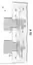
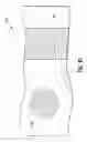
FIG. 1Fi shows a top-down view of the structure 100 of FIG. 1F, in accordance with embodiments of the present invention.
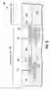
Next, in one embodiment, the solder bump 170 and the solder wall 172 of FIG. 1F are reflowed at a high temperature, resulting in structure 100 of FIG. 1G. Illustratively, the solder bump 170 and the solder wall 172 of FIG. 1F are reflowed by subjecting them to a temperature lower than 400° C.
Next, in one embodiment, the chip dicing process is performed wherein a blade (not shown) can be used to cut through the dicing channel region 104, resulting in the separated semiconductor chip 102 in FIG. 1Gi. FIG. 1Gi shows a top-down view of the chip 102 after it is cut from the structure 100 of FIG. 1G, in accordance with embodiments of the present invention. It should be noted that the chip 102 can have multiple solder bumps 170 (similar to the solder bump 170 of FIG. 1G). In one embodiment, these multiple solder bumps 170 and the solder wall 172 can be formed simultaneously using the fabrication process described above in FIGS. 1A-1G.
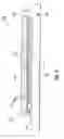
Next, with reference to FIG. 2, in one embodiment, the chip 102 is flipped upside down and bonded to a module substrate 180 (comprising ceramic in one embodiment), resulting in a module 200 in FIG. 2. In one embodiment, the multiple solder bumps 170 are bonded one-to-one to multiple substrate bump pads 182 of the ceramic module substrate 180, whereas the solder wall 172 is bonded to a substrate wall pad 184 of the ceramic module substrate 180. It should be noted that the chip 102 in FIG. 2 is a cross-section view along a line 2-2 in FIG. 1Gi.
In one embodiment, other chips (not shown, but similar to the chip 102 of FIG. 1Gi) can be bonded to the same ceramic module substrate 180 in a similar manner so as to form the multi-chip module 200.
In summary, after the chip 102 is bonded to the ceramic module substrate 180, the solder bumps 170 of the chip 102 are isolated from carbon dioxide and water vapor of the surrounding ambient environment by the chip 102, the ceramic module substrate 180, and the solder wall 172.
While particular embodiments of the present invention have been described herein for purposes of illustration, many modifications and changes will become apparent to those skilled in the art. Accordingly, the appended claims are intended to encompass all such modifications and changes as fall within the true spirit and scope of this invention.
Claims
1. A semiconductor structure, comprising:
(a) a first semiconductor chip;
(b) N solder bumps in direct physical contact with the first semiconductor chip, wherein N is a positive integer; and
(c) a first solder wall on a perimeter of the first semiconductor chip such that the first solder wall forms a closed loop surrounding the N solder bumps.
2. The structure of claim 1, further comprising a module substrate coupled to the first solder wall and the N solder bumps,
wherein the module substrate includes N substrate bump pads such that the N solder bumps are electrically coupled one-to-one to the N substrate bump pads, and
wherein the N solder bumps are isolated from a surrounding ambient environment by the first semiconductor chip, the first solder wall, and the module substrate.
3. The structure of claim 2, further comprising:
(i) a second semiconductor chip,
(ii) M solder bumps in direct physical contact with the second semiconductor chip, wherein M is a positive integer, and
(iii) a second solder wall on a perimeter of the second semiconductor chip such that the second solder wall forms a closed loop surrounding the M solder bumps,
wherein the module substrate further includes M substrate bump pads such that the M solder bumps are electrically coupled one-to-one to the M substrate bump pads of the module substrate, and
wherein the M solder bumps are isolated from the surrounding ambient environment by the second semiconductor chip, the second solder wall, and the module substrate.
4. The structure of claim 2, wherein the module substrate comprises ceramic.
5. The structure of claim 1,
wherein the first semiconductor chip comprises a crack stop on a perimeter of the first semiconductor chip, and
wherein the first solder wall is overlapping the crack stop.
6. The structure of claim 1, wherein the first solder wall and the N solder bumps comprises a same material.
7. The structure of claim 6, wherein the same material comprises a mixture of tin and lead.
8. The structure of claim 1, wherein the first semiconductor chip comprises N bump limiting metallurgy regions being in direct physical contact with the N solder bumps.
9. A semiconductor fabrication method, comprising:
providing a first semiconductor chip;
forming N solder bumps in direct physical contact with the first semiconductor chip, wherein N is a positive integer; and
forming a first solder wall on a perimeter of the first semiconductor chip such that the first solder wall forms a closed loop surrounding the N solder bumps.
10. The method of claim 9, wherein said forming the N solder bumps and said forming the first solder wall are performed simultaneously.
11. The method of claim 9, wherein said forming the N solder bumps and said forming the first solder wall are performed by using electroplating.
12. The method of claim 9, further comprising bonding the first solder wall and the N solder bumps to a module substrate,
wherein the module substrate includes N substrate bump pads such that the N solder bumps are electrically coupled one-to-one to the N substrate bump pads, and
wherein the N solder bumps are isolated from a surrounding ambient environment by the first semiconductor chip, the first solder wall, and the module substrate.
13. The structure of claim 12, further comprising:
providing (i) a second semiconductor chip, (ii) M solder bumps in direct physical contact with the second semiconductor chip, wherein M is a positive integer, and (iii) a second solder wall on a perimeter of the second semiconductor chip such that the second solder wall forms a closed loop surrounding the M solder bumps; and
bonding the second solder wall and the M solder bumps to the module substrate, such that the M solder bumps are isolated from the surrounding ambient environment by the second semiconductor chip, the second solder wall, and the module substrate.
14. The method of claim 9,
wherein the first semiconductor chip comprises a crack stop on a perimeter of the first semiconductor chip, and
wherein the first solder wall is overlapping the crack stop.
15. The method of claim 9, wherein the first solder wall and the N solder bumps comprises a same material.
16. The method of claim 15, wherein the same material comprises a mixture of tin and lead.
17. The method of claim 9, wherein the first semiconductor chip comprises N bump limiting metallurgy regions being in direct physical contact with the N solder bumps.
18. A semiconductor structure, comprising:
(a) a first semiconductor chip comprising a crack stop on a perimeter of the first semiconductor chip;
(b) N solder bumps in direct physical contact with the first semiconductor chip, wherein N is a positive integer;
(c) a first solder wall on a perimeter of the first semiconductor chip
such that the first solder wall forms a closed loop surrounding the N solder bumps, and
such that the first solder wall is overlapping the crack stop; and
(d) a module substrate coupled to the first solder wall and the N solder bumps.
19. The structure of claim 18, wherein the module substrate comprises ceramic.
20. The structure of claim 18, wherein the first solder wall and the N solder bumps comprises a mixture of tin and lead.
Images & Drawings included:

Sources:
- United States Patent and Trademark Office - verify current appl. status at the USPTO↗
Recent applications in this class:
- » 20250273612 2025-08-28
PACKAGE COMPRISING A SUBSTRATE INCLUDING AN INTER SUBSTRATE INTERCONNECT STRUCTURE COMPRISING AN INNER INTERCONNECT - » 20250266383 2025-08-21
CONDUCTIVE BUMP STRUCTURE AND MANUFACTURING METHOD THEREOF - » 20250259954 2025-08-14
SOLDER BALL, SEMICONDUCTOR PACKAGE INCLUDING THE SAME, AND METHOD OF MANUFACTURING THE SAME - » 20250259953 2025-08-14
SEMICONDUCTOR PACKAGE - » 20250226344 2025-07-10
CORE BALL AND SEMICONDUCTOR PACKAGE INCLUDING THE SAME - » 20250226343 2025-07-10
ELECTRONIC DEVICE - » 20250218997 2025-07-03
COPPER PILLAR BUMP STRUCTURE AND METHOD OF MANUFACTURING THE SAME - » 20250218996 2025-07-03
COPPER PILLAR BUMP STRUCTURE AND METHOD OF MANUFACTURING THE SAME - » 20250218995 2025-07-03
COPPER PILLAR BUMP STRUCTURE AND METHOD OF MANUFACTURING THE SAME - » 20250218994 2025-07-03
COPPER PILLAR BUMP STRUCTURE AND METHOD OF MANUFACTURING THE SAME
Recent applications for this Assignee:
- » 20250294045 2025-09-18
THREAT POLICY FINE-TUNING BASED ON THE VULNERABILITY OF A SUBNET AS A SOURCE OF A MALICIOUS ATTACK - » 20250294041 2025-09-18
DEVICE POPULATION ANOMALY DETECTION - » 20250292574 2025-09-18
SCENE PARSING - » 20250292026 2025-09-18
A GENERATIVE ARTIFICIAL INTELLIGENCE COMMENTARY - » 20250291689 2025-09-18
MACHINE LEARNING MODEL TRAINING TO ASSIST IN SYSTEM DEBUG - » 20250287215 2025-09-11
PORTABLE MEDIA GEOFENCE AND DEVICE PAIRING SECURITY - » 20250285610 2025-09-11
RECIPIENT-SPECIFIC VOICE TONE ADJUSTMENT IN TELEPHONY - » 20250284728 2025-09-11
CONTEXT LARGE LANGUAGE MODEL OUTPUT EXPLANATION - » 20250278669 2025-09-04
COUNTERFACTUALS WITH FEATURE PREFERENCES FOR CONSISTENT AND DIVERSE EXPLANATIONS - » 20250274345 2025-08-28
MULTI-LAYER EDGE ARCHITECTURE SIMULATION