MOSFET power package
US20070246772A1
2007-10-25
11/396,407
2006-03-31
Abstract:
A power MOSFET package is disclosed. The power MOSFET package includes a leadframe having first and second die pads insulated one from the other, the first die pad being coupled to a first drain lead and the second die pad being coupled to a second drain lead. A first MOSFET device has a drain contact coupled-to the first die pad, a gate contact coupled to a first gate lead, and a source contact coupled to the second die pad. A second MOSFET device has a drain contact coupled to the second die pad, a gate contact coupled to a second gate lead, and a source contact coupled to a source lead. An encapsulant substantially encapsulates the leadframe, the first and second MOSFET devices and portions of the first and second gate leads, the first and second drain leads, and the source lead.
Inventors:
- James LEE 13 🇹🇼 Taipei, Taiwan
- Tommy Ro 1 🇹🇼 Taipei, Taiwan
- Alice Gong 1 🇨🇳 Pudong, China
Interested in similar patents?
Get notified when new applications in this technology area are published.
Classification:
H01L23/49562 » CPC main
Details of semiconductor or other solid state devices; Arrangements for conducting electric current to or from the solid state body in operation, e.g. leads, terminal arrangements ; Selection of materials therefor consisting of soldered constructions; Lead-frames or other flat leads; Geometry of the lead-frame for devices being provided for in
H01L23/49575 » CPC further
Details of semiconductor or other solid state devices; Arrangements for conducting electric current to or from the solid state body in operation, e.g. leads, terminal arrangements ; Selection of materials therefor consisting of soldered constructions; Lead-frames or other flat leads Assemblies of semiconductor devices on lead frames
H01L24/06 » CPC further
Arrangements for connecting or disconnecting semiconductor or solid-state bodies; Methods or apparatus related thereto; Means for bonding being attached to, or being formed on, the surface to be connected, e.g. chip-to-package, die-attach, "first-level" interconnects; Manufacturing methods related thereto; Bonding areas ; Manufacturing methods related thereto; Structure, shape, material or disposition of the bonding areas prior to the connecting process of a plurality of bonding areas
H01L24/49 » CPC further
Arrangements for connecting or disconnecting semiconductor or solid-state bodies; Methods or apparatus related thereto; Means for bonding being attached to, or being formed on, the surface to be connected, e.g. chip-to-package, die-attach, "first-level" interconnects; Manufacturing methods related thereto; Wire connectors; Manufacturing methods related thereto; Structure, shape, material or disposition of the wire connectors after the connecting process of a plurality of wire connectors
H01L24/48 » CPC further
Arrangements for connecting or disconnecting semiconductor or solid-state bodies; Methods or apparatus related thereto; Means for bonding being attached to, or being formed on, the surface to be connected, e.g. chip-to-package, die-attach, "first-level" interconnects; Manufacturing methods related thereto; Wire connectors; Manufacturing methods related thereto; Structure, shape, material or disposition of the wire connectors after the connecting process of an individual wire connector
H01L2224/0603 » CPC further
Indexing scheme for arrangements for connecting or disconnecting semiconductor or solid-state bodies and methods related thereto as covered by; Means for bonding being attached to, or being formed on, the surface to be connected, e.g. chip-to-package, die-attach, "first-level" interconnects; Manufacturing methods related thereto; Bonding areas; Manufacturing methods related thereto; Structure, shape, material or disposition of the bonding areas prior to the connecting process of a plurality of bonding areas; Structure Bonding areas having different sizes, e.g. different heights or widths
H01L2224/06051 » CPC further
Indexing scheme for arrangements for connecting or disconnecting semiconductor or solid-state bodies and methods related thereto as covered by; Means for bonding being attached to, or being formed on, the surface to be connected, e.g. chip-to-package, die-attach, "first-level" interconnects; Manufacturing methods related thereto; Bonding areas; Manufacturing methods related thereto; Structure, shape, material or disposition of the bonding areas prior to the connecting process of a plurality of bonding areas; Shape Bonding areas having different shapes
H01L2924/01006 » CPC further
Indexing scheme for arrangements or methods for connecting or disconnecting semiconductor or solid-state bodies as covered by; Chemical elements Carbon [C]
H01L2924/01015 » CPC further
Indexing scheme for arrangements or methods for connecting or disconnecting semiconductor or solid-state bodies as covered by; Chemical elements Phosphorus [P]
H01L2924/01033 » CPC further
Indexing scheme for arrangements or methods for connecting or disconnecting semiconductor or solid-state bodies as covered by; Chemical elements Arsenic [As]
H01L2924/01082 » CPC further
Indexing scheme for arrangements or methods for connecting or disconnecting semiconductor or solid-state bodies as covered by; Chemical elements Lead [Pb]
H01L2924/014 » CPC further
Indexing scheme for arrangements or methods for connecting or disconnecting semiconductor or solid-state bodies as covered by; Alloys Solder alloys
H01L2924/19042 » CPC further
Indexing scheme for arrangements or methods for connecting or disconnecting semiconductor or solid-state bodies as covered by; Details of hybrid assemblies other than the semiconductor or other solid state devices to be connected; Structure; Component type being an inductor
H01L2224/85399 » CPC further
Indexing scheme for arrangements for connecting or disconnecting semiconductor or solid-state bodies and methods related thereto as covered by; Methods for connecting semiconductor or other solid state bodies using means for bonding being attached to, or being formed on, the surface to be connected using a wire connector; Bonding interfaces outside the semiconductor or solid-state body Material
H01L2224/05599 » CPC further
Indexing scheme for arrangements for connecting or disconnecting semiconductor or solid-state bodies and methods related thereto as covered by; Means for bonding being attached to, or being formed on, the surface to be connected, e.g. chip-to-package, die-attach, "first-level" interconnects; Manufacturing methods related thereto; Bonding areas; Manufacturing methods related thereto; Structure, shape, material or disposition of the bonding areas prior to the connecting process of an individual bonding area; External layer Material
H01L2924/00014 » CPC further
Indexing scheme for arrangements or methods for connecting or disconnecting semiconductor or solid-state bodies as covered by; Technical content checked by a classifier the subject-matter covered by the group, the symbol of which is combined with the symbol of this group, being disclosed without further technical details
H01L2224/45099 » CPC further
Indexing scheme for arrangements for connecting or disconnecting semiconductor or solid-state bodies and methods related thereto as covered by; Means for bonding being attached to, or being formed on, the surface to be connected, e.g. chip-to-package, die-attach, "first-level" interconnects; Manufacturing methods related thereto; Wire connectors; Manufacturing methods related thereto; Structure, shape, material or disposition of the wire connectors prior to the connecting process of an individual wire connector; Core members of the connector Material
H01L2924/00 » CPC further
Indexing scheme for arrangements or methods for connecting or disconnecting semiconductor or solid-state bodies as covered by
H01L2924/13091 » CPC further
Indexing scheme for arrangements or methods for connecting or disconnecting semiconductor or solid-state bodies as covered by; Details of semiconductor or other solid state devices to be connected; Device type; Discrete devices, e.g. 3 terminal devices; Transistor; Field-effect transistor [FET] Metal-Oxide-Semiconductor Field-Effect Transistor [MOSFET]
H01L2924/00012 » CPC further
Indexing scheme for arrangements or methods for connecting or disconnecting semiconductor or solid-state bodies as covered by; Technical content checked by a classifier Relevant to the scope of the group, the symbol of which is combined with the symbol of this group
H01L29/76 IPC
Semiconductor devices adapted for rectifying, amplifying, oscillating or switching, or capacitors or resistors with at least one potential-jump barrier or surface barrier, e.g. PN junction depletion layer or carrier concentration layer; Details of semiconductor bodies or of electrodes thereof; Multistep manufacturing processes therefor; Types of semiconductor device ; Multistep manufacturing processes therefor controllable by only the electric current supplied, or only the electric potential applied, to an electrode which does not carry the current to be rectified, amplified or switched Unipolar devices, e.g. field effect transistors
H01L23/495 IPC
Details of semiconductor or other solid state devices; Arrangements for conducting electric current to or from the solid state body in operation, e.g. leads, terminal arrangements ; Selection of materials therefor consisting of soldered constructions Lead-frames or other flat leads
H01L23/48 IPC
Details of semiconductor or other solid state devices Arrangements for conducting electric current to or from the solid state body in operation, e.g. leads, terminal arrangements ; Selection of materials therefor
Description
BACKGROUND OF THE INVENTION
The present invention generally relates to a MOSFET power package and more particularly to a 5-lead TO-252 power MOSFET package for use in implementing a synchronous buck converter.
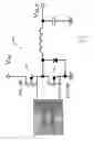
Synchronous buck converters provide a smaller size and higher efficiency in portable battery-operated applications including notebook computer applications. A conventional synchronous buck converter is shown in FIG. 2 and generally designated 200. A first N-channel enhancement MOSFET 210 is coupled to a second N-channel enhancement MOSFET 220 in a conventional manner wherein the source of the first MOSFET 210 is connected to the drain of the second MOSFET 220.
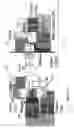
While it is known to provide two power MOSFETs in a TO-252 package in a common drain configuration as shown in FIG. 1, the synchronous buck converter 200 is conventionally implemented with discreet components and requires a large amount of printed circuit board (PCB) space. As shown in FIG. 3, a high side MOSFET 300 and a low side MOSFET 310 are surface mounted to the PCB and coupled to other circuit components including an inductor 333.
As electronic devices are miniaturized, a need exists for smaller package sizes and optimized device lead layout to save PCB space. There is therefore a need in the art for a power MOSFET package for use in implementing a synchronous buck converter that optimizes device lead layout and saves PCB space. There is also a need for a 5-lead TO-252 power MOSFET package for use in implementing a synchronous buck converter.
SUMMARY OF THE INVENTION
The present invention provides a 5-lead TO-252 power MOSFET package for implementing a synchronous buck converter that reduces package size and optimizes lead layout to save PCB space.
In accordance with one aspect of the invention, a power MOSFET package includes a leadframe having first and second die pads insulated one from the other, the first die pad being coupled to a first drain lead and the second die pad being coupled to a second drain lead. A first MOSFET device has a drain contact coupled to the first die pad, a gate contact coupled to a first gate lead, and a source contact coupled to the second die pad. A second MOSFET device has a drain contact coupled to the second die pad, a gate contact coupled to a second gate lead, and a source contact coupled to a source lead. An encapsulant substantially encapsulates the leadframe, the first and second MOSFET devices and portions of the first and second gate leads, the first and second drain leads, and the source lead.
In accordance with another aspect of the invention, a power MOSFET package for providing power and synchronous switching to a synchronous buck converter circuit includes a leadframe having first and second die pads insulated one from the other, the first die pad being coupled to a first drain lead and the second die pad being coupled to a second drain lead. A first MOSFET device has a drain contact coupled to the first die pad, a gate contact coupled to a first gate lead, and a source contact coupled to the second die pad. A second MOSFET device has a drain contact coupled to the second die pad, a gate contact coupled to a second gate lead, and a source contact coupled to a source lead. An encapsulant substantially encapsulating the leadframe, the first and second MOSFET devices and portions of the first and second gate leads, the first and second drain leads, and the source lead.
There has been outlined, rather broadly, the more important features of the invention in order that the detailed description thereof that follows may be better understood, and in order that the present contribution to the art may be better appreciated. There are, of course, additional features of the invention that will be described below and which will form the subject matter of the claims appended herein.
In this respect, before explaining at least one embodiment of the invention in detail, it is to be understood that the invention is not limited in its application to the details of the method set forth in the following description or illustrated in the drawings. The invention is capable of other embodiments and of being practiced and carried out in various ways. Also, it is to be understood that the phraseology and terminology employed herein, as well as the abstract, are for the purpose of description and should not be regarded as limiting.
As such, those skilled in the art will appreciate that the conception upon which this disclosure is based may readily be utilized as a basis for the designing of other structures, methods and systems for carrying out the several purposes of the present invention. It is important, therefore, that the claims be regarded as including such equivalent constructions insofar as they do not depart from the spirit and scope of the present invention.
These and other features, aspects and advantages of the present invention will become better understood with reference to the following drawings, description and claims.
BRIEF DESCRIPTION OF THE DRAWINGS
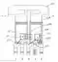
FIG. 1 is a schematic representation of a prior art TO-252 package leadframe;
FIG. 1A is a top view of a TO-252 package of the prior art;
FIG. 2 is a circuit diagram of a synchronous buck converter;
FIG. 3 is a PCB layout of a prior art synchronous buck converter;
FIG. 4 is a PCB layout of a synchronous buck converter in accordance with the invention;
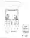
FIG. 5 is a schematic representation of a TO-252 package leadframe in accordance with the invention; and
FIG. 5A is a top view of a TO-252 package in accordance with the invention.
DETAILED DESCRIPTION OF THE INVENTION
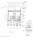
The present invention provides a TO-252 power MOSFET package for use in implementing a synchronous buck converter. With reference to FIG. 5, a TO-252 package leadframe 500 includes a pair of drain pads 510 and 520 having disposed thereon MOSFETs 515 and 525 respectively. Drain pads 510 and 520 are insulated from each other after a connecting portion 505 is trimmed off along dashed line A-A at the end of the packaging process. MOSFETs 515 and 520 are preferably soldered to drain pads 510 and 520 respectively or, alternatively, attached using conductive epoxy.
Wire bonding 530 connects the source of MOSFET 515 to the drain pad 520. A gate of MOSFET 515 is wire bonded to gate lead G1 by wire bond 517, a gate of MOSFET 525 is wire bonded to gate lead G2 by wire bond 527, and a source of MOSFET 525 is wire bonded to source lead S2 by wire bonding 540. A lead D1 is coupled to drain pad 510 while a lead D2/S1 is coupled to drain pad 520.
A TO-252 package 550 in accordance with the invention is shown in FIG. 5A and includes headers 560 and a plastic molding 570. In use, and as shown in FIG. 4, the package 550 may be used to implement a synchronous buck converter 400. The synchronous buck converter 400 using the package 550 uses less PCB space in comparison to the conventional PCB layout shown in FIG. 3. The package 550 advantageously provides an optimized lead layout. Including a 5-lead TO-252 package configuration.
It should be understood, of course, that the foregoing relates to preferred embodiments of the invention and that modifications may be made without departing from the spirit and scope of the invention as set forth in the following claims.
Claims
We claim:1. A power MOSFET package comprising:
a leadframe having first and second die pads insulated one from the other, the first die pad being coupled to a first drain lead and the second die pad being coupled to a second drain lead;
a first MOSFET device having a drain contact coupled to the first die pad, a gate contact coupled to a first gate lead, and a source contact coupled to the second die pad;
a second MOSFET device having a drain contact coupled to the second die pad, a gate contact coupled to a second gate lead, and a source contact coupled to a source lead; and
an encapsulant substantially encapsulating the leadframe, the first and second MOSFET devices and portions of the first and second gate leads, the first and second drain leads, and the source lead.
2. The power MOSFET package of claim 1, wherein the package is a TO-252 package.
3. The power MOSFET package of claim 1, wherein the package is operable to provide power and synchronous switching to a synchronous buck converter circuit.
4. A power MOSFET package for providing power and synchronous switching to a synchronous buck converter circuit comprising:
a leadframe having first and second die pads insulated one from the other, the first die pad being coupled to a first drain lead and the second die pad being coupled to a second drain lead;
a first MOSFET device having a drain contact coupled to the first die pad, a gate contact coupled to a first gate lead, and a source contact coupled to the second die pad;
a second MOSFET device having a drain contact coupled to the second die pad, a gate contact coupled to a second gate lead, and a source contact coupled to a source lead; and
an encapsulant substantially encapsulating the leadframe, the first and second MOSFET devices and portions of the first and second gate leads, the first and second drain leads, and the source lead.
5. The power MOSFET package of claim 4, wherein the package is a TO-252 package.
Images & Drawings included:
Sources:
- United States Patent and Trademark Office - verify current appl. status at the USPTO↗
Similar patent applications:
- » 20050012117
Power MOSFET, power MOSFET packaged device, and method of manufacturing power MOSFET - » 20130193520
Power MOSFET package - » 20100289092
Power MOSFET package - » 20110143499
Vertically packaged MOSFET and IC power devices as integrated module using 3D interconnected laminates - » 20210217681
Packaging structure of a SiC MOSFET power module and manufacturing method thereof - » 20080166837
Power MOSFET wafer level chip-scale package - » 20130200952
Power MOSFETs with improved efficiency for multi-channel class D audio amplifiers and packaging therefor - » 20140203870
Power MOSFETs with improved efficiency for multi-channel class D audio amplifiers and packaging therefor - » 20160142018
POWER MOSFETS WITH IMPROVED EFFICIENCY FOR MULTI-CHANNEL CLASS D AUDIO AMPLIFIERS AND PACKAGING THEREFOR - » 20110156229
Semiconductor device package having a semiconductor chip on wiring board connected to plurality of leads including power MOSFETs
Recent applications in this class:
- » 20250174527 2025-05-29
SEMICONDUCTOR DEVICE - » 20250167081 2025-05-22
REVERSIBLE POWER MODULE AND A PROCESS OF IMPLEMENTING A REVERSIBLE POWER MODULE - » 20250157896 2025-05-15
INTEGRATED CIRCUIT DEVICE - » 20250112132 2025-04-03
SEMICONDUCTOR PACKAGE HAVING LEAD FRAME WITH SLANTED SECTIONS - » 20250105108 2025-03-27
SEMICONDUCTOR DEVICE COMPRISING A SEMICONDUCTOR DIE SANDWICHED BETWEEN TWO LEADFRAMES AND A METHOD FOR FABRICATING THE SAME - » 20250096083 2025-03-20
SEMICONDUCTOR PACKAGE - » 20250096082 2025-03-20
INTERCONNECT CLIP FOR VERTICALLY STACKED DIE ARRANGEMENT - » 20250096081 2025-03-20
SEMICONDUCTOR PACKAGE HAVING INTERPOSER AND METHOD OF MAKING THE SAME - » 20250069997 2025-02-27
SEMICONDUCTOR DEVICE - » 20250062196 2025-02-20
SEMICONDUCTOR DEVICE AND METHOD OF FORMING COMPONENTS FOR SEMICONDUCTOR DEVICE