Power semiconductor module
US20080105896A1
2008-05-08
11/566,274
2006-12-04
✅ Patent granted
US 7,514,777 B2
2009-04-07
-
-
Evan Pert | Selim Ahmed
2026-12-04
Abstract:
A power semiconductor module of the present invention comprises: a heat sink 1; a circuit substrate 2 mounted on the heat sink 1; a conductive pattern 10 provided on the circuit substrate 2; a low dielectric constant film 11 covering the conductive pattern 10; a case 7 provided on the heat sink 1 so as to enclose the circuit substrate 2; and a soft insulator 9 filling the space within the case 7. The low dielectric constant film 11 is preferably formed of silicon rubber, polyimide, or epoxy resin.
Assignee:
- MITSUBISHI ELECTRIC CORPORATION 16,560 🇯🇵 TOKYO, Japan
- Mitsubishi Electric Corporation 2,856 🇯🇵 Chiyoda-ku, Japan
Interested in similar patents?
Get notified when new applications in this technology area are published.
Classification:
H01L23/5385 » CPC main
Details of semiconductor or other solid state devices; Arrangements for conducting electric current within the device in operation from one component to another, i.e. interconnections, e.g. wires, lead frames the interconnection structure between a plurality of semiconductor chips being formed on, or in, insulating substrates Assembly of a plurality of insulating substrates
H01L24/49 » CPC further
Arrangements for connecting or disconnecting semiconductor or solid-state bodies; Methods or apparatus related thereto; Means for bonding being attached to, or being formed on, the surface to be connected, e.g. chip-to-package, die-attach, "first-level" interconnects; Manufacturing methods related thereto; Wire connectors; Manufacturing methods related thereto; Structure, shape, material or disposition of the wire connectors after the connecting process of a plurality of wire connectors
H01L25/162 » CPC further
Assemblies consisting of a plurality of individual semiconductor or other solid state devices ; Multistep manufacturing processes thereof the devices being of types provided for in two or more different main groups of - , e.g. forming hybrid circuits the devices being mounted on two or more different substrates
H01L24/45 » CPC further
Arrangements for connecting or disconnecting semiconductor or solid-state bodies; Methods or apparatus related thereto; Means for bonding being attached to, or being formed on, the surface to be connected, e.g. chip-to-package, die-attach, "first-level" interconnects; Manufacturing methods related thereto; Wire connectors; Manufacturing methods related thereto; Structure, shape, material or disposition of the wire connectors prior to the connecting process of an individual wire connector
H01L24/48 » CPC further
Arrangements for connecting or disconnecting semiconductor or solid-state bodies; Methods or apparatus related thereto; Means for bonding being attached to, or being formed on, the surface to be connected, e.g. chip-to-package, die-attach, "first-level" interconnects; Manufacturing methods related thereto; Wire connectors; Manufacturing methods related thereto; Structure, shape, material or disposition of the wire connectors after the connecting process of an individual wire connector
H01L25/072 » CPC further
Assemblies consisting of a plurality of individual semiconductor or other solid state devices ; Multistep manufacturing processes thereof all the devices being of a type provided for in the same subgroup of groups - , e.g. assemblies of rectifier diodes the devices not having separate containers the devices being of a type provided for in group the devices being arranged next to each other
H01L25/18 » CPC further
Assemblies consisting of a plurality of individual semiconductor or other solid state devices ; Multistep manufacturing processes thereof the devices being of types provided for in two or more different subgroups of the same main group of groups -
H01L2224/8592 » CPC further
Indexing scheme for arrangements for connecting or disconnecting semiconductor or solid-state bodies and methods related thereto as covered by; Methods for connecting semiconductor or other solid state bodies using means for bonding being attached to, or being formed on, the surface to be connected using a wire connector; Post-treatment of the connector or wire bonding area Applying permanent coating, e.g. protective coating
H01L2924/01006 » CPC further
Indexing scheme for arrangements or methods for connecting or disconnecting semiconductor or solid-state bodies as covered by; Chemical elements Carbon [C]
H01L2924/01013 » CPC further
Indexing scheme for arrangements or methods for connecting or disconnecting semiconductor or solid-state bodies as covered by; Chemical elements Aluminum [Al]
H01L2924/01014 » CPC further
Indexing scheme for arrangements or methods for connecting or disconnecting semiconductor or solid-state bodies as covered by; Chemical elements Silicon [Si]
H01L2924/01029 » CPC further
Indexing scheme for arrangements or methods for connecting or disconnecting semiconductor or solid-state bodies as covered by; Chemical elements Copper [Cu]
H01L2924/01033 » CPC further
Indexing scheme for arrangements or methods for connecting or disconnecting semiconductor or solid-state bodies as covered by; Chemical elements Arsenic [As]
H01L2924/01058 » CPC further
Indexing scheme for arrangements or methods for connecting or disconnecting semiconductor or solid-state bodies as covered by; Chemical elements Cerium [Ce]
H01L2924/01068 » CPC further
Indexing scheme for arrangements or methods for connecting or disconnecting semiconductor or solid-state bodies as covered by; Chemical elements Erbium [Er]
H01L2924/01082 » CPC further
Indexing scheme for arrangements or methods for connecting or disconnecting semiconductor or solid-state bodies as covered by; Chemical elements Lead [Pb]
H01L2924/014 » CPC further
Indexing scheme for arrangements or methods for connecting or disconnecting semiconductor or solid-state bodies as covered by; Alloys Solder alloys
H01L2924/00014 » CPC further
Indexing scheme for arrangements or methods for connecting or disconnecting semiconductor or solid-state bodies as covered by; Technical content checked by a classifier the subject-matter covered by the group, the symbol of which is combined with the symbol of this group, being disclosed without further technical details
H01L2924/13055 » CPC further
Indexing scheme for arrangements or methods for connecting or disconnecting semiconductor or solid-state bodies as covered by; Details of semiconductor or other solid state devices to be connected; Device type; Discrete devices, e.g. 3 terminal devices; Transistor; Bipolar Junction Transistor [BJT] Insulated gate bipolar transistor [IGBT]
H01L2924/1305 » CPC further
Indexing scheme for arrangements or methods for connecting or disconnecting semiconductor or solid-state bodies as covered by; Details of semiconductor or other solid state devices to be connected; Device type; Discrete devices, e.g. 3 terminal devices; Transistor Bipolar Junction Transistor [BJT]
H01L2924/181 » CPC further
Indexing scheme for arrangements or methods for connecting or disconnecting semiconductor or solid-state bodies as covered by; Details of package parts other than the semiconductor or other solid state devices to be connected Encapsulation
H01L2924/00 » CPC further
Indexing scheme for arrangements or methods for connecting or disconnecting semiconductor or solid-state bodies as covered by
H01L31/111 IPC
Semiconductor devices sensitive to infra-red radiation, light, electromagnetic radiation of shorter wavelength or corpuscular radiation and specially adapted either for the conversion of the energy of such radiation into electrical energy or for the control of electrical energy by such radiation; Processes or apparatus specially adapted for the manufacture or treatment thereof or of parts thereof; Details thereof in which radiation controls flow of current through the device, e.g. photoresistors characterised by at least one potential-jump barrier or surface barrier, e.g. phototransistors; Devices sensitive to infra-red, visible or ultra-violet radiation characterised by at least three potential barriers, e.g. photothyristor
H01L23/34 IPC
Details of semiconductor or other solid state devices Arrangements for cooling, heating, ventilating or temperature compensation ; Temperature sensing arrangements
Description
BACKGROUND OF THE INVENTION
1. Field of the Invention
The present invention relates to a power semiconductor module in which partial discharge is reduced to achieve a longer operating life.
2. Background Art
A conventional power semiconductor module, such as that proposed in Japanese Laid-Open Patent Publication No. 2002-76197, includes: a heat sink; a circuit substrate(s) mounted on the heat sink; a conductive pattern provided on the circuit substrate; a case provided on the heat sink so as to enclose the circuit substrate; a soft insulator filling the space within the case; and a solid insulator provided on the top surface of the circuit substrate such that it is in contact with the peripheral portion of the conductive pattern. The solid insulator is intended to enhance the insulation resistance and the withstand voltage of the module.
However, when the power semiconductor module is used at a high voltage, a partial discharge may occur from a floating potential portion within the module, resulting in insulation failure. It has been found that drive circuit substrates having electrodes on both sides and having a complicated shape are especially susceptible to partial discharge.
SUMMARY OF THE INVENTION
The present invention has been devised to solve the above problem. It is, therefore, an object of the present invention to provide a power semiconductor module in which partial discharge is reduced to achieve a longer operating life.
According to one aspect of the present invention, a power semiconductor module of the present invention comprises: a heat sink; a circuit substrate mounted on the heat sink; a conductive pattern provided on the circuit substrate; a low dielectric constant film covering the conductive pattern; a case provided on the heat sink so as to enclose the circuit substrate; and a soft insulator filling the space within the case. The low dielectric constant film is preferably formed of silicon rubber, polyimide, or epoxy resin.
The present invention allows reduction of partial discharge within a power semiconductor module, resulting in an extended operating life.
Other and further objects, features and advantages of the invention will appear more fully from the following description.
BRIEF DESCRIPTION OF THE DRAWINGS
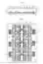
FIG. 1 is a cross-sectional view of a power semiconductor module according to a first embodiment of the present invention.
FIG. 2 is a top view of the power semiconductor module according to the first embodiment of the present invention.
FIG. 3 shows an equivalent circuit of a circuit block in the power semiconductor module shown in FIG. 2.
FIG. 4 is an enlarged cross-sectional view of a portion A shown in FIG. 1.
FIG. 5 is a top view of a drive circuit substrate according to a second embodiment of the present invention.
FIG. 6 is a top view of a drive circuit substrate according to a third embodiment of the present invention.
FIG. 7 is a top view of a drive circuit substrate according to a fourth embodiment of the present invention.
DETAILED DESCRIPTION OF THE PREFERRED EMBODIMENTS
First Embodiment
FIG. 1 is a cross-sectional view of a power semiconductor module according to a first embodiment of the present invention, and FIG. 2 is a top view of the module. This power semiconductor module comprises a plurality of circuit blocks each including a plurality of parallel-connected IGBTs that share common collector, emitter, and gate terminals to achieve high electrical strength and high current operation. For reference, FIG. 3 shows an equivalent circuit of such a circuit block.
Referring to FIGS. 1 and 2, drive circuit substrates 2 (circuit substrates), power semiconductor circuit substrates 3, and junction circuit substrates 13 are mounted on a metal base plate 1 (a heat sink). Each circuit substrate includes an insulating substrate of a ceramic material, etc. and a conductive (or electrode) pattern 10 of copper or aluminum, etc. formed on both sides of the insulating substrate. Power semiconductor devices (chips) 4, such as insulated gate bipolar transistors (IGBTs) 4a and freewheel diodes 4b, are bonded onto the conductive pattern of each power semiconductor circuit substrate 3 by a conductive adhesive member, such as solder. On the other hand, chip resistances 14 are bonded onto the conductive pattern of each drive circuit substrate 2 by a conductive adhesive member such as solder. Electrodes of the power semiconductor devices 4 (namely, the emitter and gate of each IGBT 4a and the anode of each freewheel diode 4b) are electrically connected to their respective drive circuit substrates 2 or junction circuit substrates 13 by wires 5 of Al, etc. More specifically, the emitter electrodes of the IGBTs 4a and the anode electrodes of the freewheel diodes 4b are connected to the conductive pattern 10 of their respective junction circuit substrates 13 by wires 5, while the gate electrodes of the IGBTs 4a are connected to the conductive pattern 10 of their respective drive circuit substrates 2 by wires 5. On each power semiconductor circuit substrate 3, the cathode electrodes of the freewheel diodes 4b are connected to the collector of their respective IGBTs 4a through the conductive pattern 10. A plastic case 7 is provided on the base plate 1 so as to enclose the drive circuit substrates 2, the power semiconductor circuit substrates 3, and the junction circuit substrates 13. A lid 8 is disposed on the top of the case 7. Further, the space within the case 7 is filled with a silicon gel 9 (soft insulator) to make the case 7 airtight and insulate the components inside. Further, each circuit substrate includes an electrode terminal bonding region 15 on which electrode terminals (not shown in the figures) are mounted to allow electrical connection to external devices. It should be noted that although in the above example the power semiconductor circuit substrates 3 and the junction circuit substrates 13 are separately provided, they may be combined into a single insulating substrate that has thereon separate conductive pattern formation regions for power semiconductor circuits and for junction circuits.
FIG. 4 is an enlarged cross-sectional view of a portion A (i.e., a drive circuit substrate 2) shown in FIG. 1. A conductive pattern 10 formed of a metal such as copper or aluminum is provided on the drive circuit substrate 2. A low dielectric constant film 11 is provided so as to cover the conductive pattern 10. This arrangement reduces partial discharge on the drive circuit substrate 2 having a complicated shape, allowing the operating life of the product to be extended. It should be noted that unlike the drive circuit substrates 2, there is no need to cover the conductive patterns on the power semiconductor circuit substrates 3 and the junction circuit substrates 13. The insulation resistance and the withstand voltage of these circuit substrates can be enhanced by providing a low dielectric constant film 11 on the top surface of each insulating substrate such that it is in contact with the peripheral portion of the conductive pattern, as in conventional arrangements.
It should be noted that the low dielectric constant films 11 may be formed of silicon rubber, polyimide, or epoxy resin. Each material has its advantages. For example, the use of silicon rubber facilitates the assembly, polyimide provides enhanced heat resistance, and epoxy resin provides enhanced heat cycle characteristics.
A brief description will be made of a process of forming a low dielectric constant film 11. In the case of a drive circuit substrate 2, first, chip resistances 14 are bonded at predetermined positions on the conductive pattern on the drive circuit substrate 2 by solder, etc. Then, aluminum wires are connected between the wire bonding positions on the conductive pattern of the drive circuit substrate 2 and the power semiconductor devices 4 (specifically, the gate electrodes of IGBTs 4a) on a power semiconductor circuit substrate 3 (in the same circuit block) by ultrasonic bonding, etc. Then, after bonding electrode terminals to the electrode terminal bonding region 15 of the conductive pattern 10 by solder, etc., a low dielectric constant film 11 is formed so as to cover the conductive pattern 10. On the other hand, in the case of a power semiconductor circuit substrate 3 (and a junction circuit substrate 13), a low dielectric constant film 11 is formed as follows. First, power semiconductor devices 4 are bonded at predetermined positions on the conductor pattern of the power semiconductor circuit substrate 3 by solder, etc. Then, before bonding wires and electrode terminals, a low dielectric constant film 11 is formed on the top surface of the insulating substrate such that it is in contact with the peripheral portion of the conductive pattern.
Second Embodiment
FIG. 5 is a top view of a drive circuit substrate according to a second embodiment of the present invention. According to the second embodiment, the conductive pattern 10 has round corners. All other components are similar to those described in connection with the first embodiment. This embodiment allows further reduction of partial discharge on the drive circuit substrate, resulting in a longer operating life of the product, as compared to the first embodiment.
Third Embodiment
FIG. 6 is a top view of a drive circuit substrate according to a third embodiment of the present invention. According to the third embodiment, the conductive pattern 10 has a round shape and is not covered with a low dielectric constant film 11. All other components are similar to those described in connection with the first embodiment. This embodiment also allows reduction of partial discharge on the drive circuit substrate 2 (which has a complicated shape), resulting in an extended operating life of the product.
Fourth Embodiment
FIG. 7 is a top view of a drive circuit substrate according to a fourth embodiment of the present invention. According to the fourth embodiment, the conductive pattern 10 is covered with a low dielectric constant film 11. Except for this feature, the drive circuit substrate is similar to that of the third embodiment. The present embodiment allows further reduction of partial discharge on the drive circuit substrate, resulting in a longer operating life of the product, as compared to the third embodiment.
Obviously many modifications and variations of the present invention are possible in the light of the above teachings. It is therefore to be understood that within the scope of the appended claims the invention may be practiced otherwise than as specifically described.
The entire disclosure of a Japanese Patent Application No. 2006-265178, filed on Sep. 28, 2006 including specification, claims, drawings and summary, on which the Convention priority of the present application is based, are incorporated herein by reference in its entirety.
Claims
What is claimed is:1. A power semiconductor module comprising:
a heat sink;
a circuit substrate mounted on the heat sink;
a conductive pattern provided on the circuit substrate;
a low dielectric constant film covering the conductive pattern;
a case provided on the heat sink so as to enclose the circuit substrate;
a lid disposed on a top portion of the case; and
a soft insulator filling the space within the case.
2. The power semiconductor module as claimed in claim 1, wherein the low dielectric constant film is formed of silicon rubber, polyimide, or epoxy resin.
3. The power semiconductor module as claimed in claim 1, the conductive pattern has a round corner.
4. The power semiconductor module as claimed in claim 2, the conductive pattern has a round corner.
5. A power semiconductor module comprising:
a heat sink;
a circuit substrate mounted on the heat sink;
a conductive pattern provided on the circuit substrate and having a round shape;
a case provided on the heat sink so as to enclose the circuit substrate; and
a soft insulator filling the space within the case.
6. The power semiconductor module as claimed in claim 5, further comprising a low dielectric constant film covering the conductive pattern.
Images & Drawings included:


Sources:
- United States Patent and Trademark Office - verify current appl. status at the USPTO↗
Similar patent applications:
- » 20220139797
Semiconductor module, power semiconductor module, and power electronic equipment using the semiconductor module or the power semiconductor module - » 20100252922
Power semiconductor module, power semiconductor module assembly and method for fabricating a power semiconductor module assembly - » 20240260168
CIRCUIT BOARD FOR A POWER SEMICONDUCTOR MODULE, POWER SEMICONDUCTOR MODULE, AND METHOD FOR PRODUCING A CIRCUIT BOARD AND A POWER SEMICONDUCTOR MODULE - » 20230155479
Power semiconductor module, power electronic assembly including one or more power semiconductor modules, and power conversion control circuit for a power semiconductor module - » 20140225245
Power semiconductor module and power semiconductor module assembly with multiple power semiconductor modules - » 20250259909
A HEAT DISSIPATION SUBSTRATE FOR A POWER SEMICONDUCTOR MODULE, A POWER SEMICONDUCTOR MODULE INCLUDING THE SAME AND A POWER CONVERTER INCLUDING THE SAME, AND MANUFACTURING METHOD OF THE HEAT DISSIPATION SUBSTRATE FOR A POWER SEMICONDUCTOR MODULE - » 20250259908
HEAT DISSIPATION SUBSTRATE FOR A POWER SEMICONDUCTOR MODULE, A POWER SEMICONDUCTOR MODULE INCLUDING THE SAME AND A POWER CONVERTER INCLUDING THE SAME, AND MANUFACTURING METHOD OF THE HEAT DISSIPATION SUBSTRATE FOR A POWER SEMICONDUCTOR MODULE - » 20250118636
HEAT DISSIPATION SUBSTRATE FOR A POWER SEMICONDUCTOR MODULE, A POWER SEMICONDUCTOR MODULE INCLUDING THE HEAT DISSIPATION SUBSTRATE, AND A POWER CONVERTER INCLUDING THE POWER SEMICONDUCTOR MODULE - » 20250118680
HEAT DISSIPATION SUBSTRATE FOR A POWER SEMICONDUCTOR MODULE, A POWER SEMICONDUCTOR MODULE INCLUDING THE HEAT DISSIPATION SUBSTRATE, AND A POWER CONVERTER INCLUDING THE POWER SEMICONDUCTOR MODULE - » 20230170287
POWER SEMICONDUCTOR MODULE, METHOD FOR ASSEMBLING A POWER SEMICONDUCTOR MODULE AND HOUSING FOR A POWER SEMICONDUCTOR MODULE
Recent applications in this class:
- » 20250293170 2025-09-18
MICROELECTRONIC ASSEMBLIES WITH DIRECT ATTACH TO CIRCUIT BOARDS - » 20250293169 2025-09-18
STACKABLE POWER SEMICONDUCTOR MODULE - » 20250293168 2025-09-18
SEMICONDUCTOR DEVICE WITH INTEGRATED VOLTAGE REGULATOR - » 20250293167 2025-09-18
THREE-DIMENSIONAL STRUCTURE BOARD - » 20250273581 2025-08-28
PACKAGE STRUCTURE WITH UNDERFILL - » 20250273580 2025-08-28
POWER MODULE AND METHOD FOR PRODUCING A POWER MODULE - » 20250259936 2025-08-14
ELECTRONIC MODULE, METHOD OF MANUFACTURING ELECTRONIC MODULE AND ELECTRONIC MODULE MANUFACTURING DEVICE - » 20250259935 2025-08-14
ELECTRONIC MODULE - » 20250259934 2025-08-14
ELECTRONIC MODULE AND METHOD OF MANUFACTURING ELECTRONIC MODULE - » 20250253256 2025-08-07
ELECTRONIC MODULE AND ELECTRONIC APPARATUS
Recent applications for this Assignee:
- » 20250294680 2025-09-18
POWER MODULE - » 20250293740 2025-09-18
WIRELESS COMMUNICATION SYSTEM - » 20250293196 2025-09-18
SEMICONDUCTOR DEVICE AND MANUFACTURING METHOD THEREOF - » 20250291113 2025-09-18
OPTICAL TERMINATOR, OPTICAL WAVELENGTH FILTER, AND EXTERNAL CAVITY LASER LIGHT SOURCE - » 20250290867 2025-09-18
SEMICONDUCTOR INSPECTION APPARATUS AND METHOD OF MANUFACTURING SEMICONDUCTOR DEVICE - » 20250290765 2025-09-18
INFORMATION PROCESSING DEVICE, INFORMATION PROCESSING METHOD, AND IMAGE PROJECTING SYSTEM - » 20250289592 2025-09-18
SPACE SITUATIONAL AWARENESS BUSINESS DEVICE AND SPACE TRAFFIC BUSINESS DEVICE - » 20250287683 2025-09-11
SEMICONDUCTOR DEVICE - » 20250287624 2025-09-11
POWER SEMICONDUCTOR DEVICE - » 20250287098 2025-09-11
DETECTION DEVICE, CAMERA SYSTEM, DETECTION METHOD, AND STORAGE MEDIUM STORING DETECTION PROGRAM