Component arrangement comprising a carrier
US20080111216A1
2008-05-15
11/860,556
2007-09-25
✅ Patent granted
US 7,911,039 B2
2011-03-22
-
-
Nitin Parekh
2029-03-09
Abstract:
A component arrangement comprising a carrier, a component in a housing with electrical contacts and a moulding compound that encloses the carrier, the semiconductor component in the housing and the electrical contacts, wherein the component is applied on the carrier, and wherein the carrier is provided with holes, and a method for producing a component arrangement, wherein the carrier is provided with holes, the component is positioned on the carrier, the component is connected to the carrier, the component with the carrier is positioned in the leadframe, and this arrangement is enclosed by a moulding compound.
Inventors:
- Joachim Mahler 223 🇩🇪 Regensburg, Germany
- Alfred Haimerl 40 🇩🇪 Sinzing, Germany
- Michael Bauer 97 🇩🇪 Nittendorf, Germany
- Angela Kessler 25 🇩🇪 Regensburg, Germany
- Wolfgang Schober 31 🇩🇪 Amberg, Germany
Assignee:
- INFINEON TECHNOLOGIES AG 8,942 🇩🇪 Neubiberg, Germany
- INFINEON TECHNOLOGIES AG 173 🇩🇪 Muenchen, Germany
Interested in similar patents?
Get notified when new applications in this technology area are published.
Classification:
H01L2924/00014 » CPC further
Indexing scheme for arrangements or methods for connecting or disconnecting semiconductor or solid-state bodies as covered by; Technical content checked by a classifier the subject-matter covered by the group, the symbol of which is combined with the symbol of this group, being disclosed without further technical details
H01L2924/207 » CPC further
Indexing scheme for arrangements or methods for connecting or disconnecting semiconductor or solid-state bodies as covered by; Parameters Diameter ranges
H01L23/495 IPC
Details of semiconductor or other solid state devices; Arrangements for conducting electric current to or from the solid state body in operation, e.g. leads, terminal arrangements ; Selection of materials therefor consisting of soldered constructions Lead-frames or other flat leads
H05K3/284 » CPC main
Apparatus or processes for manufacturing printed circuits; Secondary treatment of printed circuits; Applying non-metallic protective coatings for encapsulating mounted components
H05K3/284 » CPC main
Apparatus or processes for manufacturing printed circuits; Secondary treatment of printed circuits; Applying non-metallic protective coatings for encapsulating mounted components
H01L23/3107 » CPC further
Details of semiconductor or other solid state devices; Encapsulations, e.g. encapsulating layers, coatings, e.g. for protection characterised by the arrangement or shape the device being completely enclosed
H01L23/4334 » CPC further
Details of semiconductor or other solid state devices; Arrangements for cooling, heating, ventilating or temperature compensation ; Temperature sensing arrangements; Fillings or auxiliary members in containers or encapsulations selected or arranged to facilitate heating or cooling; Auxiliary members in containers characterised by their shape, e.g. pistons Auxiliary members in encapsulations
H01L23/49531 » CPC further
Details of semiconductor or other solid state devices; Arrangements for conducting electric current to or from the solid state body in operation, e.g. leads, terminal arrangements ; Selection of materials therefor consisting of soldered constructions; Lead-frames or other flat leads; Additional leads the additional leads being a wiring board
H01L25/162 » CPC further
Assemblies consisting of a plurality of individual semiconductor or other solid state devices ; Multistep manufacturing processes thereof the devices being of types provided for in two or more different main groups of - , e.g. forming hybrid circuits the devices being mounted on two or more different substrates
H01L24/48 » CPC further
Arrangements for connecting or disconnecting semiconductor or solid-state bodies; Methods or apparatus related thereto; Means for bonding being attached to, or being formed on, the surface to be connected, e.g. chip-to-package, die-attach, "first-level" interconnects; Manufacturing methods related thereto; Wire connectors; Manufacturing methods related thereto; Structure, shape, material or disposition of the wire connectors after the connecting process of an individual wire connector
H01L2924/01068 » CPC further
Indexing scheme for arrangements or methods for connecting or disconnecting semiconductor or solid-state bodies as covered by; Chemical elements Erbium [Er]
H01L2924/19041 » CPC further
Indexing scheme for arrangements or methods for connecting or disconnecting semiconductor or solid-state bodies as covered by; Details of hybrid assemblies other than the semiconductor or other solid state devices to be connected; Structure; Component type being a capacitor
H01L2924/19105 » CPC further
Indexing scheme for arrangements or methods for connecting or disconnecting semiconductor or solid-state bodies as covered by; Details of hybrid assemblies other than the semiconductor or other solid state devices to be connected; Disposition of discrete passive components in a side-by-side arrangement on a common die mounting substrate
H01L2924/19107 » CPC further
Indexing scheme for arrangements or methods for connecting or disconnecting semiconductor or solid-state bodies as covered by; Details of hybrid assemblies other than the semiconductor or other solid state devices to be connected; Disposition of discrete passive components off-chip wires
H01L2924/3025 » CPC further
Indexing scheme for arrangements or methods for connecting or disconnecting semiconductor or solid-state bodies as covered by; Technical effects; Electrical effects Electromagnetic shielding
H05K1/0306 » CPC further
Printed circuits; Details; Use of materials for the substrate Inorganic insulating substrates, e.g. ceramic, glass
H05K1/0306 » CPC further
Printed circuits; Details; Use of materials for the substrate Inorganic insulating substrates, e.g. ceramic, glass
H05K1/142 » CPC further
Printed circuits; Details; Structural association of two or more printed circuits Arrangements of planar printed circuit boards in the same plane, e.g. auxiliary printed circuit insert mounted in a main printed circuit
H05K1/142 » CPC further
Printed circuits; Details; Structural association of two or more printed circuits Arrangements of planar printed circuit boards in the same plane, e.g. auxiliary printed circuit insert mounted in a main printed circuit
H05K2201/09063 » CPC further
Indexing scheme relating to printed circuits covered by; Shape and layout; Substrate related Holes or slots in insulating substrate not used for electrical connections
H05K2201/09063 » CPC further
Indexing scheme relating to printed circuits covered by; Shape and layout; Substrate related Holes or slots in insulating substrate not used for electrical connections
H05K2201/09072 » CPC further
Indexing scheme relating to printed circuits covered by; Shape and layout; Substrate related Hole or recess under component or special relationship between hole and component
H05K2201/09072 » CPC further
Indexing scheme relating to printed circuits covered by; Shape and layout; Substrate related Hole or recess under component or special relationship between hole and component
H05K2201/1034 » CPC further
Indexing scheme relating to printed circuits covered by; Details of components or other objects attached to or integrated in a printed circuit board; Other objects, e.g. metallic pieces Edge terminals, i.e. separate pieces of metal attached to the edge of the PCB
H05K2201/1034 » CPC further
Indexing scheme relating to printed circuits covered by; Details of components or other objects attached to or integrated in a printed circuit board; Other objects, e.g. metallic pieces Edge terminals, i.e. separate pieces of metal attached to the edge of the PCB
H05K2201/10977 » CPC further
Indexing scheme relating to printed circuits covered by; Details of components or other objects attached to or integrated in a printed circuit board; Details of electrical connections of non-printed components, e.g. special leads; Other details of electrical connections Encapsulated connections
H05K2203/049 » CPC further
Indexing scheme relating to apparatus or processes for manufacturing printed circuits covered by; Soldering or other types of metallurgic bonding Wire bonding
H05K2203/049 » CPC further
Indexing scheme relating to apparatus or processes for manufacturing printed circuits covered by; Soldering or other types of metallurgic bonding Wire bonding
H01L2924/00 » CPC further
Indexing scheme for arrangements or methods for connecting or disconnecting semiconductor or solid-state bodies as covered by
H01L2924/14 » CPC further
Indexing scheme for arrangements or methods for connecting or disconnecting semiconductor or solid-state bodies as covered by; Details of semiconductor or other solid state devices to be connected; Device type Integrated circuits
H01L2924/181 » CPC further
Indexing scheme for arrangements or methods for connecting or disconnecting semiconductor or solid-state bodies as covered by; Details of package parts other than the semiconductor or other solid state devices to be connected Encapsulation
H01L2924/00012 » CPC further
Indexing scheme for arrangements or methods for connecting or disconnecting semiconductor or solid-state bodies as covered by; Technical content checked by a classifier Relevant to the scope of the group, the symbol of which is combined with the symbol of this group
H01L2224/45099 » CPC further
Indexing scheme for arrangements for connecting or disconnecting semiconductor or solid-state bodies and methods related thereto as covered by; Means for bonding being attached to, or being formed on, the surface to be connected, e.g. chip-to-package, die-attach, "first-level" interconnects; Manufacturing methods related thereto; Wire connectors; Manufacturing methods related thereto; Structure, shape, material or disposition of the wire connectors prior to the connecting process of an individual wire connector; Core members of the connector Material
H01L21/56 IPC
Processes or apparatus adapted for the manufacture or treatment of semiconductor or solid state devices or of parts thereof; Manufacture or treatment of semiconductor devices or of parts thereof the devices having at least one potential-jump barrier or surface barrier, e.g. PN junction, depletion layer or carrier concentration layer; Assembly of semiconductor devices using processes or apparatus not provided for in a single one of the subgroups - , e.g. sealing of a cap to a base of a container Encapsulations, e.g. encapsulation layers, coatings
Description
The invention relates to a component arrangement comprising at least one carrier, and a method for producing the component arrangement.
Semiconductor components, such as integrated circuits or individual semiconductors, are generally applied on a carrier. The semiconductor component is encapsulated by a moulding compound. The cured moulding compound gives the semiconductor component a desired form, protects the semiconductor component against environmental influences and enables a robust identification of the encapsulated semiconductor component. Strips which are connected to bonding wires and which are not completely encapsulated by the moulding compound enable electrical contact externally.
In terms of its composition, the moulding compound should be configured in such a way that it completely encapsulates the semiconductor component and reliably adheres on the surface of the semiconductor component and of the carrier. In addition, the moulding compound must be constituted in such a way that it can reliably flow around all irregularities of the arrangement with the semiconductor component and the carrier and can penetrate into any void or any gap in said arrangement.
The size of the particles of the moulding compound, the granulation, should be chosen such that the moulding compound can penetrate into any gap. If the granulation of the moulding compound is not small enough, then the problem can occur that only the resins of the moulding compound penetrate into small gaps in the arrangement or the gaps are blocked by fillers. The unfilled cavities resulting from this reduce the reliability of the component arrangement.
Arrangements composed of electrical components and carriers that are to be encapsulated with moulding compound have irregular elevations and gaps which make it more difficult for moulding compound to flow around said arrangements.
Therefore, the present invention is based on the object of configuring an arrangement composed of semiconductor components or other electrical components, such as capacitors or coils, and carriers in such a way that said arrangement is completely encapsulated by the moulding compound.
According to the invention, this object is achieved by means of a component arrangement having the features of claim 1 and by means of a method having the features of Claim 8. The subclaims each define preferred advantageous embodiments.
Embodiments of the invention are explained in more detail below with reference to the accompanying drawings, in which
FIG. 1 shows the side view in section of an exemplary embodiment with one component on one carrier,
FIG. 2 shows the side view in section of an exemplary embodiment with two components on one carrier,
FIG. 3 shows the plan view in section of an exemplary embodiment with a plurality of components on one carrier,
FIG. 4 shows the side view in section of an exemplary embodiment with a plurality of components on two or more carriers,
FIG. 5 shows the side view in section of an exemplary embodiment with a plurality of components on two or more carriers,
FIG. 6 shows the plan view in section of an exemplary embodiment with a plurality of components on two carriers,
FIG. 7 shows the plan view in section of an exemplary embodiment with a plurality of components on a plurality of carriers.
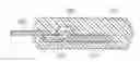
FIG. 1 shows a side view in section of a component arrangement comprising a carrier 100, comprising a semiconductor component 200, a plurality of contact strips 300, which is encapsulated by a moulding compound. The contact strips 300 are directly connected to the carrier 100. An electrical connection between the carrier 100 and the contact strips 300 can be obtained by means of a solder. The carrier 100 can be a carrier such as is usually used for the mounting of electronic components. Such a carrier is referred to as a PCB (printed circuit board). Electronic components are positioned on a PCB, fixed by means of a solder and electrically connected to the PCB. Arrangements on a PCB can be sprayed or encapsulated with a resin by moulding in order to shield said arrangement from environmental influences.
At least one semiconductor component 200 is applied on the carrier 100, said component, for its part, being situated in a housing. This arrangement is subsequently encapsulated by moulding with a moulding compound, which also gives this arrangement the external form.
Externally, the finished component arrangement can no longer be distinguished from a conventional electronic component.
A hole 500 can be introduced in the carrier below a component 200. The component arrangement in FIG. 1 therefore comprises a carrier, a component in a housing, electrical contacts and a moulding compound that encloses the carrier, the component in the housing and the electrical contacts, wherein the component is applied on the carrier, and wherein the carrier is provided with holes. With regard to the electrical contacts of the component arrangement, it should thus be understood that the electrical contacts are only partly enclosed by the moulding compound.
In FIG. 1, the hole is arranged directly below the component 200. By virtue of this arrangement, the moulding compound of the component arrangement can also pass below the component 200. A narrow gap into which the moulding compound cannot penetrate is thus avoided. The hole can be configured in such a way that it merely makes it easier for the moulding compound to fill the cavity below the component 200. If the diameter of the hole is larger than the gap between the component 200 and the carrier 100, it is ensured that the moulding compound can penetrate into the gap. A further configuration is to configure the hole in such a way that the entire region below the component 200 is open, such that a relatively large gap does not arise below the component 200. This configuration of the carrier of the component arrangement affords the particular advantage that a special moulding compound does not have to be used. Thus, this arrangement according to the invention can also be encapsulated by a moulding compound that does not have particularly fine granulation.
FIG. 2 shows a side view in section of a component arrangement comprising a carrier 100, comprising a semiconductor component 200, comprising a passive component 210 and a plurality of contact strips 300, which is encapsulated by a moulding compound. The contact strips 300 are directly connected to the carrier 100.
The passive component 210 bears directly on the carrier 200. If a component bears so closely on the carrier 100 that no gap arises below the component, then it is not necessary to provide a hole below the component. This fact is illustrated by the component 210 in FIG. 2.
FIG. 3 shows a plan view in section of a component arrangement comprising a carrier 100, comprising a semiconductor component 200, comprising a passive component 210, a further component 220 and a plurality of contact strips 300. The contact strips 300 are directly connected to the carrier 100. The exemplary embodiment in FIG. 3 shows how holes are to be arranged on a carrier 100. A hole is present below each component 200, 210, 220 in order that the cavities below said components can be reliably filled with the moulding compound. A further hole 510 is provided in addition to the holes 500 below the components. In the component arrangement in FIG. 3, the components 200, 210, 220 form a barrier that impedes the inflow of the moulding compound for encapsulating the arrangement. One possibility for enabling the unimpeded inflow of the moulding compound is to arrange the components 200, 210, 220 differently on the carrier 100. This appears to be readily possible in the case of a simple exemplary embodiment as in FIG. 3. However, such a rearrangement of the components is generally associated with disadvantages. The most significant disadvantage is that the components can no longer be optimally arranged electrically on the carrier 100. The hole 510 shown in FIG. 3 has the particular advantage that the components 200, 210, 220 can be arranged in such a way that the entire component arrangement in FIG. 3 has optimal electrical properties. The hole 510 in FIG. 3 serves to enable the moulding compound to flow around the components 200, 210, 220, or to control the flow of moulding compound in such a way that no cavities arise in the component arrangement. In FIG. 3, the hole has a circular form; a different form is also possible. Thus, by way of examples the hole can also be embodied as an elongated rectangle extending over the carrier. Furthermore, an arrangement of a plurality of holes lying alongside one another is also possible in order to enable the inflow of moulding compound.
FIG. 4 shows a side view in section of a component arrangement comprising a carrier 100, comprising a semiconductor component 200, comprising a passive component 210, a further carrier 110, comprising a component 230 and a plurality of contact strips 300, which is encapsulated by a moulding compound. The contact strips 300 are directly connected to the carrier 100. The carrier 110 is electrically connected to the carrier 100 by means of bonding wires.
In the exemplary embodiment in FIG. 4, the carrier 110 is a DCB carrier (DCB: direct copper bonding), on the surface of which is applied a semiconductor component 230 without a housing. A DCB carrier is a carrier comprising a plurality of metallic layers and at least one ceramic layer (or electrically insulating layer). Such DCB carriers have the advantage that the electrical conductivity of the carrier is very low and the thermal conductivity of the carrier is very high.
FIG. 4 therefore shows a component arrangement in which semiconductor components in housings, passive components and power semiconductor components without a housing are arranged on a plurality of carriers, which is encapsulated in shaping fashion by a moulding compound. This component arrangement reveals the advantage afforded by forming the holes in at least one carrier; all the components can be arranged in such a way that good electrical properties of the component arrangement result.
FIG. 5 shows a component arrangement as in FIG. 4 with the difference that the carrier 100 is not directly connected to the contact strips 300. The electrical connection is effected by means of bonding wires in this exemplary embodiment. The component arrangement can be configured even more flexibly by virtue of connection by means of bonding wires.
FIG. 6 shows a plan view in section of a component arrangement comprising a carrier 100, comprising a semiconductor component 200, comprising a passive component 210, a further component 220, a plurality of contact strips 300 and a further carrier 110, which is encapsulated by a moulding compound. The contact strips 300 are connected to the carrier 100 by means of bonding wires. The exemplary embodiment in FIG. 4 shows how holes can be arranged on a carrier 100. A hole is present below each component 200, 210, 220 in order that the cavities below said components can be reliably filled with the moulding compound. Further holes 510 are provided in addition to the holes 500 below the components. In the component arrangement in FIG. 6, the components 200, 210, 220 form a barrier that impedes the inflow of moulding compound for encapsulating the arrangement. The holes 510 shown in FIG. 6 have the particular advantage that the components 200, 210, 220 can be arranged in such a way that the entire component arrangement in FIG. 6 has optimal electrical properties. The holes 510 in FIG. 6 serve to enable the moulding compound to flow around the components 200, 210, 220. In FIG. 6, the hole has a rectangular form, other forms also being possible.
FIG. 7 shows a plan view of a component arrangement comprising a carrier 100, comprising a semiconductor component 200, comprising a passive component 210, a further component 220, a plurality of contact strips 300 and two further carriers 120, 130, which is encapsulated by a moulding compound. The contact strips 300 are directly connected to the carrier 100. The exemplary embodiment in FIG. 7 shows how holes can be arranged on a carrier 100. A hole is present below each component 200, 210, 220 in order that the cavities below said components can be reliably filled with the moulding compound. Further holes are provided in addition to the holes 500 below the components. In the component arrangement in FIG. 7, the components 240 form a barrier that impedes the inflow of moulding compound for encapsulating the arrangement. The holes 500, 510 shown in FIG. 7 have the particular advantage that the components 240 can be arranged in such a way that the entire component arrangement in FIG. 7 has optimal electrical properties. The holes 510 in FIG. 7 serve to enable the moulding compound to flow around the components 240. In FIG. 7, a hole has a rectangular form, other forms also being possible.
Claims
1. Component arrangement comprising:
a carrier,
a component in a housing,
electrical contacts,
a moulding compound that completely encloses the carrier and the component in the housing and partly encloses the electrical contacts,
wherein the component is applied on the carrier, and
wherein the carrier is provided with holes.
2. Component arrangement according to claim 1, wherein the component in the housing is a semiconductor component.
3. Component arrangement according claim 1, wherein a second carrier with an applied semiconductor component is partly enclosed by the moulding compound.
4. Component arrangement according to claim 1, wherein the electrical contacts are directly connected to the carrier.
5. Component arrangement according to claim 1, wherein the electrical contacts are directly connected to the carrier by means of a bonding wire.
6. Component arrangement according to claim 1, wherein the holes are formed below the components.
7. Component arrangement according to claim 1, wherein the holes are formed alongside the component.
8. Method for producing a component arrangement comprising the steps of:
providing a carrier with holes,
positioning a component on the carrier,
connecting the component to the carrier,
forming an arrangement by positioning the component with the carrier in a leadframe,
cleaning the arrangement with plasma and activating the surface of the carrier,
enclosing the arrangement in a moulding compound, and
isolating the enclosed arrangement from the leadframe.
Images & Drawings included:


Sources:
- United States Patent and Trademark Office - verify current appl. status at the USPTO↗
Similar patent applications:
- » 20110135255
Arrangement comprising an electrical conductor track carrier and an optoelectronic component, and a method for producing such an arrangement - » 20250170798
Interior Component Comprising a Carrier Element and a Textile Top Layer Arranged on the Carrier Element, and a Method for Producing the Interior Component - » 20240001395
Method for applying a coating to at least one electronic component, sensor arrangement comprising a coating and coating carrier - » 20250065355
METHOD FOR APPLYING A COATING TO AT LEAST ONE ELECTRONIC COMPONENT, SENSOR ARRANGEMENT COMPRISING A COATING AND COATING CARRIER
Recent applications in this class:
- » 20250212339 2025-06-26
AUTOCLAVABLE ELECTRONICS UNIT FOR AN ENDOSCOPE, METHOD FOR PRODUCING AN AUTOCLAVABLE ELECTRONICS UNIT AND ENDOSCOPE - » 20250212338 2025-06-26
POWER TOOL, POWER DEVICE, AND BATTERY PACK - » 20250185179 2025-06-05
INTRISICALLY SAFE DESIGNED DEVICES AND METHODS THEREFOR - » 20250168990 2025-05-22
METHOD FOR MANUFACTURING TRIM PANELS FOR VEHICLES HAVING AN ELECTRONIC FUNCTION - » 20250048560 2025-02-06
COATING AGENT AND METHOD FOR MANUFACTURING MODULE USING THE COATING AGENT - » 20240431037 2024-12-26
DESIGN OF A RECYCLABLE ELECTRONIC DEVICE - » 20240334614 2024-10-03
ELECTRICAL DEVICE HAVING HEAT DISSIPATION STRUCTURE USING FILLER AND MANUFACTURING METHOD OF THE SAME - » 20240306310 2024-09-12
IMPLANTABLE MEDICAL DEVICE CASE FIT WITH SELECTIVE ENCAPSULATION - » 20240306309 2024-09-12
BARRIER LAYER FOR AN ELECTRICAL DEVICE - » 20240276649 2024-08-15
POWER SUPPLY MODULE AND METHOD OF ASSEMBLY
Recent applications for this Assignee:
- » 20250293127 2025-09-18
LEADFRAME PANEL, A SEMICONDUCTOR PACKAGE COMPRISING A LEADFRAME WITH A TWO-LEVEL DAMBAR DESIGN AND A METHOD FOR FABRICATING THE SAME - » 20250285937 2025-09-11
HOUSING, SEMICONDUCTOR MODULE COMPRISING A HOUSING, AND METHOD FOR ASSEMBLING A SEMICONDUCTOR MODULE - » 20250279324 2025-09-04
PACKAGE WITH CARRIER HAVING COMPONENT ACCOMMODATION VOLUME ON ONE SIDE AND REPELLING STRUCTURE ON OTHER SIDE - » 20250266310 2025-08-21
ENCAPSULANT WITH LOW CTE AND LOW YOUNG MODULUS FOR LOW-STRESS ELECTRONIC PACKAGE - » 20250258195 2025-08-14
TEST PIN WITH POGO PIN AND SURROUNDING COIL SPRING FOR TESTING DEVICES UNDER TEST - » 20250257469 2025-08-14
METAL COMPONENT INCLUDING AN INTERMETALLIC COMPOUND LAYER AND METHOD FOR MANUFACTURING THEREOF - » 20250253195 2025-08-07
HOUSING FOR A SEMICONDUCTOR MODULE, SEMICONDUCTOR MODULE COMPRISING A HOUSING, AND METHOD FOR ASSEMBLING A SEMICONDUCTOR MODULE COMPRISING A HOUSING - » 20250240890 2025-07-24
METHOD OF EMBEDDING AN EMBEDDABLE OBJECT INTO A STACKED SUBSTRATE AND STACKED SUBSTRATE ARRANGEMENT - » 20250226297 2025-07-10
PACKAGE WITH CARRIER HAVING PLATED BOTTOM SURFACE AND SIDEWALL - » 20250219841 2025-07-03
SECURE COMMUNICATIONS USING PRE-SHARED KEYS AND LIVE MEMBERSHIP