Inverted lead frame in substrate
US20080150106A1
2008-06-26
11/959,519
2007-12-19
✅ Patent granted
US 7,642,638 B2
2010-01-05
-
-
Luan C Thai
2028-06-24
Abstract:
A semiconductor package, and method of making a semiconductor package, with a plurality of dies, wherein one die is attached to an inverted lead frame and another die is attached to a substrate. The leadframe is then attached to the substrate. More specifically, the semiconductor package includes a substrate, a lead frame and a plurality of leads. The lead frame is attached to the top surface of the substrate. The bottom surface of a first die is attached to the top surface of the substrate and the first die is electrically connected to the substrate. The top surface of a second die is attached to the bottom die pad surface of the lead frame and the second die is electrically connected to the leadframe. An encapsulant covers at least a portion of the lead frame and substrate.
Assignee:
- UNITED TEST AND ASSEMBLY CENTER LTD. 48 🇸🇬 Singapore, Singapore
Interested in similar patents?
Get notified when new applications in this technology area are published.
Classification:
H01L23/52 IPC
Details of semiconductor or other solid state devices Arrangements for conducting electric current within the device in operation from one component to another, i.e. interconnections, e.g. wires, lead frames
H01L23/02 IPC
Details of semiconductor or other solid state devices Containers; Seals
H01L23/4334 » CPC main
Details of semiconductor or other solid state devices; Arrangements for cooling, heating, ventilating or temperature compensation ; Temperature sensing arrangements; Fillings or auxiliary members in containers or encapsulations selected or arranged to facilitate heating or cooling; Auxiliary members in containers characterised by their shape, e.g. pistons Auxiliary members in encapsulations
H01L23/552 » CPC further
Details of semiconductor or other solid state devices Protection against radiation, e.g. light or electromagnetic waves
H01L24/97 » CPC further
Arrangements for connecting or disconnecting semiconductor or solid-state bodies; Methods or apparatus related thereto; Batch processes at chip-level, i.e. with connecting carried out on a plurality of singulated devices, i.e. on diced chips the devices being connected to a common substrate, e.g. interposer, said common substrate being separable into individual assemblies after connecting
H01L25/0657 » CPC further
Assemblies consisting of a plurality of individual semiconductor or other solid state devices ; Multistep manufacturing processes thereof all the devices being of a type provided for in the same subgroup of groups - , e.g. assemblies of rectifier diodes the devices not having separate containers the devices being of a type provided for in group Stacked arrangements of devices
H01L23/13 » CPC further
Details of semiconductor or other solid state devices; Mountings, e.g. non-detachable insulating substrates characterised by the shape
H01L23/3128 » CPC further
Details of semiconductor or other solid state devices; Encapsulations, e.g. encapsulating layers, coatings, e.g. for protection characterised by the arrangement or shape the device being completely enclosed a substrate forming part of the encapsulation the substrate having spherical bumps for external connection
H01L23/49816 » CPC further
Details of semiconductor or other solid state devices; Arrangements for conducting electric current to or from the solid state body in operation, e.g. leads, terminal arrangements ; Selection of materials therefor consisting of soldered constructions; Leads, on insulating substrates,; Additional leads joined to the metallisation on the insulating substrate, e.g. pins, bumps, wires, flat leads Spherical bumps on the substrate for external connection, e.g. ball grid arrays [BGA]
H01L24/48 » CPC further
Arrangements for connecting or disconnecting semiconductor or solid-state bodies; Methods or apparatus related thereto; Means for bonding being attached to, or being formed on, the surface to be connected, e.g. chip-to-package, die-attach, "first-level" interconnects; Manufacturing methods related thereto; Wire connectors; Manufacturing methods related thereto; Structure, shape, material or disposition of the wire connectors after the connecting process of an individual wire connector
H01L24/49 » CPC further
Arrangements for connecting or disconnecting semiconductor or solid-state bodies; Methods or apparatus related thereto; Means for bonding being attached to, or being formed on, the surface to be connected, e.g. chip-to-package, die-attach, "first-level" interconnects; Manufacturing methods related thereto; Wire connectors; Manufacturing methods related thereto; Structure, shape, material or disposition of the wire connectors after the connecting process of a plurality of wire connectors
H01L24/73 » CPC further
Arrangements for connecting or disconnecting semiconductor or solid-state bodies; Methods or apparatus related thereto Means for bonding being of different types provided for in two or more of groups , , , , , , ,
H01L2224/16 » CPC further
Indexing scheme for arrangements for connecting or disconnecting semiconductor or solid-state bodies and methods related thereto as covered by; Means for bonding being attached to, or being formed on, the surface to be connected, e.g. chip-to-package, die-attach, "first-level" interconnects; Manufacturing methods related thereto; Bump connectors; Manufacturing methods related thereto; Structure, shape, material or disposition of the bump connectors after the connecting process of an individual bump connector
H01L2225/0651 » CPC further
Details relating to assemblies covered by the group but not provided for in its subgroups; All the devices being of a type provided for in the same subgroup of groups - the devices not having separate containers the devices being of a type provided for in group; Stacked arrangements of devices Wire or wire-like electrical connections from device to substrate
H01L2225/06527 » CPC further
Details relating to assemblies covered by the group but not provided for in its subgroups; All the devices being of a type provided for in the same subgroup of groups - the devices not having separate containers the devices being of a type provided for in group; Stacked arrangements of devices Special adaptation of electrical connections, e.g. rewiring, engineering changes, pressure contacts, layout
H01L2225/06589 » CPC further
Details relating to assemblies covered by the group but not provided for in its subgroups; All the devices being of a type provided for in the same subgroup of groups - the devices not having separate containers the devices being of a type provided for in group; Stacked arrangements of devices Thermal management, e.g. cooling
H01L2924/01005 » CPC further
Indexing scheme for arrangements or methods for connecting or disconnecting semiconductor or solid-state bodies as covered by; Chemical elements Boron [B]
H01L2924/01006 » CPC further
Indexing scheme for arrangements or methods for connecting or disconnecting semiconductor or solid-state bodies as covered by; Chemical elements Carbon [C]
H01L2924/01027 » CPC further
Indexing scheme for arrangements or methods for connecting or disconnecting semiconductor or solid-state bodies as covered by; Chemical elements Cobalt [Co]
H01L2924/01033 » CPC further
Indexing scheme for arrangements or methods for connecting or disconnecting semiconductor or solid-state bodies as covered by; Chemical elements Arsenic [As]
H01L2924/01082 » CPC further
Indexing scheme for arrangements or methods for connecting or disconnecting semiconductor or solid-state bodies as covered by; Chemical elements Lead [Pb]
H01L2924/14 » CPC further
Indexing scheme for arrangements or methods for connecting or disconnecting semiconductor or solid-state bodies as covered by; Details of semiconductor or other solid state devices to be connected; Device type Integrated circuits
H01L2924/1433 » CPC further
Indexing scheme for arrangements or methods for connecting or disconnecting semiconductor or solid-state bodies as covered by; Details of semiconductor or other solid state devices to be connected; Device type; Integrated circuits; Digital devices Application-specific integrated circuit [ASIC]
H01L2924/15153 » CPC further
Indexing scheme for arrangements or methods for connecting or disconnecting semiconductor or solid-state bodies as covered by; Details of package parts other than the semiconductor or other solid state devices to be connected; Die mounting substrate; Shape the die mounting substrate comprising a recess for hosting the device
H01L2924/15165 » CPC further
Indexing scheme for arrangements or methods for connecting or disconnecting semiconductor or solid-state bodies as covered by; Details of package parts other than the semiconductor or other solid state devices to be connected; Die mounting substrate Monolayer substrate
H01L2924/1532 » CPC further
Indexing scheme for arrangements or methods for connecting or disconnecting semiconductor or solid-state bodies as covered by; Details of package parts other than the semiconductor or other solid state devices to be connected; Die mounting substrate; Connection portion the connection portion being formed on the die mounting surface of the substrate
H01L2924/16152 » CPC further
Indexing scheme for arrangements or methods for connecting or disconnecting semiconductor or solid-state bodies as covered by; Details of package parts other than the semiconductor or other solid state devices to be connected; Cap; Shape Cap comprising a cavity for hosting the device, e.g. U-shaped cap
H01L2224/85 » CPC further
Indexing scheme for arrangements for connecting or disconnecting semiconductor or solid-state bodies and methods related thereto as covered by; Methods for connecting semiconductor or other solid state bodies using means for bonding being attached to, or being formed on, the surface to be connected using a wire connector
H01L2224/83 » CPC further
Indexing scheme for arrangements for connecting or disconnecting semiconductor or solid-state bodies and methods related thereto as covered by; Methods for connecting semiconductor or other solid state bodies using means for bonding being attached to, or being formed on, the surface to be connected using a layer connector
H01L2924/15311 » CPC further
Indexing scheme for arrangements or methods for connecting or disconnecting semiconductor or solid-state bodies as covered by; Details of package parts other than the semiconductor or other solid state devices to be connected; Die mounting substrate; Connection portion the connection portion being formed only on the surface of the substrate opposite to the die mounting surface being a ball array, e.g. BGA
H01L2924/3025 » CPC further
Indexing scheme for arrangements or methods for connecting or disconnecting semiconductor or solid-state bodies as covered by; Technical effects; Electrical effects Electromagnetic shielding
H01L2224/97 » CPC further
Indexing scheme for arrangements for connecting or disconnecting semiconductor or solid-state bodies and methods related thereto as covered by; Batch processes at chip-level, i.e. with connecting carried out on a plurality of singulated devices, i.e. on diced chips the devices being connected to a common substrate, e.g. interposer, said common substrate being separable into individual assemblies after connecting
H01L2224/73265 » CPC further
Indexing scheme for arrangements for connecting or disconnecting semiconductor or solid-state bodies and methods related thereto as covered by; Means for bonding being of different types provided for in two or more of groups; Location after the connecting process on different surfaces Layer and wire connectors
H01L2924/00 » CPC further
Indexing scheme for arrangements or methods for connecting or disconnecting semiconductor or solid-state bodies as covered by
H01L2924/181 » CPC further
Indexing scheme for arrangements or methods for connecting or disconnecting semiconductor or solid-state bodies as covered by; Details of package parts other than the semiconductor or other solid state devices to be connected Encapsulation
H01L2924/00012 » CPC further
Indexing scheme for arrangements or methods for connecting or disconnecting semiconductor or solid-state bodies as covered by; Technical content checked by a classifier Relevant to the scope of the group, the symbol of which is combined with the symbol of this group
H01L2224/45099 » CPC further
Indexing scheme for arrangements for connecting or disconnecting semiconductor or solid-state bodies and methods related thereto as covered by; Means for bonding being attached to, or being formed on, the surface to be connected, e.g. chip-to-package, die-attach, "first-level" interconnects; Manufacturing methods related thereto; Wire connectors; Manufacturing methods related thereto; Structure, shape, material or disposition of the wire connectors prior to the connecting process of an individual wire connector; Core members of the connector Material
H01L2924/00014 » CPC further
Indexing scheme for arrangements or methods for connecting or disconnecting semiconductor or solid-state bodies as covered by; Technical content checked by a classifier the subject-matter covered by the group, the symbol of which is combined with the symbol of this group, being disclosed without further technical details
H01L2924/207 » CPC further
Indexing scheme for arrangements or methods for connecting or disconnecting semiconductor or solid-state bodies as covered by; Parameters Diameter ranges
H01L23/495 IPC
Details of semiconductor or other solid state devices; Arrangements for conducting electric current to or from the solid state body in operation, e.g. leads, terminal arrangements ; Selection of materials therefor consisting of soldered constructions Lead-frames or other flat leads
H01L21/56 IPC
Processes or apparatus adapted for the manufacture or treatment of semiconductor or solid state devices or of parts thereof; Manufacture or treatment of semiconductor devices or of parts thereof the devices having at least one potential-jump barrier or surface barrier, e.g. PN junction, depletion layer or carrier concentration layer; Assembly of semiconductor devices using processes or apparatus not provided for in a single one of the subgroups - , e.g. sealing of a cap to a base of a container Encapsulations, e.g. encapsulation layers, coatings
H01L23/34 IPC
Details of semiconductor or other solid state devices Arrangements for cooling, heating, ventilating or temperature compensation ; Temperature sensing arrangements
H01L23/10 IPC
Details of semiconductor or other solid state devices; Containers; Seals characterised by the material or arrangement of seals between parts, e.g. between cap and base of the container or between leads and walls of the container
H01L23/48 IPC
Details of semiconductor or other solid state devices Arrangements for conducting electric current to or from the solid state body in operation, e.g. leads, terminal arrangements ; Selection of materials therefor
H01L29/40 IPC
Semiconductor devices adapted for rectifying, amplifying, oscillating or switching, or capacitors or resistors with at least one potential-jump barrier or surface barrier, e.g. PN junction depletion layer or carrier concentration layer; Details of semiconductor bodies or of electrodes thereof; Multistep manufacturing processes therefor Electrodes ; Multistep manufacturing processes therefor
H01L21/50 IPC
Processes or apparatus adapted for the manufacture or treatment of semiconductor or solid state devices or of parts thereof; Manufacture or treatment of semiconductor devices or of parts thereof the devices having at least one potential-jump barrier or surface barrier, e.g. PN junction, depletion layer or carrier concentration layer Assembly of semiconductor devices using processes or apparatus not provided for in a single one of the subgroups - , e.g. sealing of a cap to a base of a container
H01L21/48 IPC
Processes or apparatus adapted for the manufacture or treatment of semiconductor or solid state devices or of parts thereof; Manufacture or treatment of semiconductor devices or of parts thereof the devices having at least one potential-jump barrier or surface barrier, e.g. PN junction, depletion layer or carrier concentration layer Manufacture or treatment of parts, e.g. containers, prior to assembly of the devices, using processes not provided for in a single one of the subgroups -
H01L21/44 IPC
Processes or apparatus adapted for the manufacture or treatment of semiconductor or solid state devices or of parts thereof; Manufacture or treatment of semiconductor devices or of parts thereof the devices having at least one potential-jump barrier or surface barrier, e.g. PN junction, depletion layer or carrier concentration layer the devices having semiconductor bodies not provided for in groups, , , and with or without impurities, e.g. doping materials Manufacture of electrodes on semiconductor bodies using processes or apparatus not provided for in groups -
Description
CROSS REFERENCES TO RELATED APPLICATIONS
This Application claims benefit of co-pending U.S. Provisional Application No. 60/871,509, filed on Dec. 22, 2006, which are incorporated herein by reference.
FIELD OF THE INVENTION
The present invention relates to a semiconductor package, and method of making a semiconductor package, with a plurality of dies, wherein one die is attached to an inverted lead frame and another die is attached to a substrate. The leadframe is then attached to the substrate.
DESCRIPTION OF THE RELATED ART
Based on current packaging trends, a stacked die package typically includes a plurality of dies packaged in a vertical stack. Conventional methods of assembling the stacked die package involves seating a smaller die on top of a larger die to create a pyramid structure such that each die does not seat on the periphery of the die immediately below it where wire bonds are placed.
A problem would arise when a smaller die such as a radio frequency (RF) die is bundled with a larger die such as an application specific integrated circuit (ASIC) die using conventional die stacking methods, and the smaller die has conductor/resistance limitations. In such packages, it is preferable that the wire bond connecting the RF die to a substrate be kept as short as possible. Conventional methods of die stacking, however, requires the smaller RF die to be stacked on top of the larger ASIC die. Therefore, the RF die being further away from the substrate relative to the ASIC die, would have a longer wire bond.
Conventional methods of forming a stacked die package can be time consuming as they require sequential implementation of the process steps involved in the package assembly.
FIG. 10B shows a conventional method for assembling a semiconductor package. In step C1, a first die (i.e., an ASIC die) is attached to a substrate using a die attach epoxy. Next, in step C2, the first die is wire bonded to the substrate. Then, in step C3, a second die (i.e., a RF die) is attached to the first die using a die attach epoxy. Next, in step C4, the second die is wire bonded to the substrate. Then, in step C5, the substrate and the wire bonded dies are molded. After the molding, in step C6, solder balls are attached to the semiconductor package. In step C7, the package is singulated. The conventional method, as mentioned above, involve process steps that occur in sequential order. It will therefore be desirable to improve the process to enable some of the steps to be carried out simultaneously so that manufacturing time can be reduced.
SUMMARY OF THE INVENTION
Exemplary embodiments of the present invention overcome the above disadvantages and other disadvantages not described above. Also, the present invention is not required to overcome the disadvantages described above, and an exemplary embodiment of the present invention may not overcome any of the problems described above.
One semiconductor package according to an embodiment of the present invention includes a substrate with a top surface and a bottom surface, a lead frame with a top die pad surface, a bottom die pad surface and a plurality of leads, wherein the lead frame is attached to the top surface of the substrate; a first die with a top surface and a bottom surface, wherein the bottom surface is attached to the top surface of the substrate and the first die is electrically connected to the substrate; a second die with a top surface and a bottom surface, wherein the top surface is attached to the bottom die pad surface of the lead frame and the second die is electrically connected to the leadframe; and an encapsulant covering at least a portion of the lead frame and substrate.
The semiconductor package may also include a third die with a top surface and a bottom surface, wherein the bottom surface is attached to the top surface of the substrate and the third die is electrically connected to the substrate.
The semiconductor package may also include a fourth die with a top surface and a bottom surface, wherein the top surface is attached to the top bottom surface of the second die and the fourth die is electrically connected to the leadframe.
The semiconductor package may also include a third die with a top surface and a bottom surface, wherein the bottom surface is attached to the top surface of the first die and the third die is electrically connected to the substrate.
The semiconductor package may also include a fourth die with a top surface and a bottom surface, wherein the top surface is attached to the bottom surface of the second die and the fourth die is electrically connected to the leadframe.
The semiconductor package may also include a third die with a top surface and a bottom surface, wherein the top surface is attached to the bottom surface of the second die; and a plurality of bond wires connected between the bottom surface of the third die and the leads on the lead frame.
The semiconductor package may also include having the encapsulant cover the entire top die pad surface of the lead frame.
The semiconductor package may also include having the encapsulant cover the entire top die pad surface of the lead frame, except for a plurality of areas.
The semiconductor package may also include a second semiconductor package that is connected to the lead frame through the plurality of areas.
The semiconductor package may also include having the top die pad surface of the lead frame have an etched area and the encapsulant cover the etched area, but not the remaining portion of the top die pad surface.
A semiconductor package according to a second embodiment of the present invention includes a lead frame with a top die pad surface, a bottom die pad surface and a plurality of leads; a substrate with a top surface, a bottom surface, and a cavity, wherein the lead frame is attached to the top surface of the substrate; a first die with a top surface and a bottom surface, wherein the bottom surface is attached to the cavity of the substrate and the first die is electrically connected to the substrate; a second die with a top surface and a bottom surface, wherein the top surface is attached to the bottom die pad surface of the lead frame and the second die is electrically connected to the leadframe; and an encapsulant covering at least a portion of the lead frame and substrate.
The semiconductor package according to the second embodiment may also include a third die with a top surface and a bottom surface, wherein the bottom surface is attached to the cavity of the substrate and the third die is electrically connected to the substrate.
The semiconductor package according to the second embodiment may also include a fourth die with a top surface and a bottom surface, wherein the top surface is attached to the bottom surface of the second die and the fourth die is electrically connected to the leadframe.
The semiconductor package according to the second embodiment may also include a third die with a top surface and a bottom surface, wherein the bottom surface is attached to the top surface of the first die and the third die is electrically connected to the substrate.
The semiconductor package according to the second embodiment may also include a fourth die with a top surface and a bottom surface, wherein the top surface is attached to the bottom surface of the second die and the fourth die is electrically connected to the leadframe.
The semiconductor package according to the second embodiment may also include a third die with a top surface and a bottom surface, wherein the top surface is attached to the bottom surface of the second die and the third die is electrically connected to the lead frame.
The semiconductor package according to the second embodiment may also include having the encapsulant cover the entire top die pad surface of the lead frame.
The semiconductor package according to the second embodiment may also include having the encapsulant cover the entire top die pad surface of the lead frame, except for a plurality of areas.
The semiconductor package according to the second embodiment may also include a second semiconductor package that is connected to the lead frame through the plurality of areas.
The semiconductor package according to the second embodiment may also include having the top die pad surface of the lead frame include a half-etched area and the encapsulant cover the half-etched area, but not the remaining portion of the top die pad surface.
A method of manufacturing a semiconductor package according to an embodiment of the invention includes (a) providing a substrate with a top surface and a bottom surface; b) providing a lead frame with a top die pad surface, a bottom die pad surface and a plurality of leads; (c) attaching a first die with a top surface and a bottom surface to the substrate, wherein the bottom surface of the first die is attached to the top surface of the substrate and the first die is electrically connected to the substrate; (d) attaching a second die with a top surface and a bottom surface to the lead frame, wherein the top surface of the second die is attached to the bottom die pad surface of the lead frame and the second die is electrically connected to the leadframe; (e) attaching the lead frame to the top surface of the substrate; and (f) encapsulating at least a portion of the lead frame and substrate.
The method of manufacturing the semiconductor package may also include attaching solder balls to said substrate and singulating said semiconductor packages into individual semiconductor packages.
The method of manufacturing the semiconductor package may also include having steps (c) and (d) occur simultaneously.
A method of manufacturing a plurality of semiconductor packages according to a second embodiment may include (a) providing a substrate strip with a top surface and a bottom surface; (b) providing a lead frame strip with top die pad surfaces, bottom die pad surfaces and a plurality of leads; (c) attaching a plurality of first dies with top surfaces and bottom surfaces to the substrate strip, wherein the bottom surfaces of the first dies are attached to the top surface of the substrate strip and the first dies are electrically connected to the substrate strip; (d) attaching a plurality of second dies with top surfaces and bottom surfaces to the lead frame, wherein the top surfaces of the second dies are attached to the bottom die pad surfaces of the lead frame strip and the second dies are electrically connected to the leadframe strip; (e) attaching the lead frame strip to the top surface of the substrate strip; and (f) encapsulating at least a portion of the lead frame strip and substrate strip.
The second method of manufacturing the semiconductor package may also include attaching solder balls to said substrate strip and singulating said semiconductor packages into individual semiconductor packages.
The second method of manufacturing the semiconductor package may also include having steps (c) and (d) occur simultaneously.
BRIEF DESCRIPTION OF THE DRAWINGS
Many aspects of the invention can be better understood with reference to the following drawings. The components in the drawings are not necessarily to scale, emphasis instead being placed upon clearly illustrating the principles of the present invention. Moreover, in the drawings, like reference numerals designate corresponding parts throughout the several views.
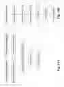
FIG. 1A shows a cross-sectional view of a first embodiment of the invention.
FIG. 1B is a cross-sectional view of a modification to the leadframe of the invention.
FIGS. 2A and 2B show cross-sectional and perspective views of an embodiment of a method of the invention.
FIGS. 3A, 3B and 3C show cross-sectional and top views of an embodiment of the leadframe and substrate of the invention.
FIG. 4 shows a cross-sectional view of a second embodiment of the invention.
FIG. 5 shows a cross-sectional view of a third embodiment of the invention.
FIG. 6 shows a cross-sectional view of a fourth embodiment of the invention.
FIG. 7 shows a cross-sectional view of a fifth embodiment of the invention.
FIG. 8 shows a cross-sectional view of a sixth embodiment of the invention.
FIGS. 9A, 9B and 9C show top and cross-sectional views of a seventh embodiment of the invention.
FIG. 10A shows an embodiment of a method of the invention.
FIG. 10B shows an embodiment of a conventional method of assembling a package.
DETAILED DESCRIPTION OF THE ILLUSTRATIVE NON-LIMITING EMBODIMENTS OF THE INVENTION
Hereinafter, the present invention will be described in detail by way of exemplary embodiments with reference to the drawings. The described exemplary embodiments are intended to assist in the understanding of the invention, and are not intended to limit the scope of the invention in any way. Throughout the drawings for explaining the exemplary embodiments, those components having identical functions carry the same reference numerals for which duplicate explanations will be omitted.
The semiconductor package of the present invention includes an inverted lead frame attached to a substrate. Each of the inverted lead frame and the substrate holds one or more dies. When the inverted leadframe is attached to the substrate, an enclosed area is formed between the inverted leadframe and the substrate and the respective one or more dies on the lead frame and on the substrate face one another. The lead frame and substrate are connected by a solder material present on the substrate or on the leads of the lead frame. The solder material can be pre-printed onto the leadframe or onto the substrate. Mold material, which encapsulates at least a portion of the lead frame and the substrate, can also hold both structures in place.
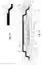
FIGS. 1A, 2A and 2B show an example of one embodiment of the semiconductor package 10 of the invention. The package includes a substrate 100 with a top surface 100a and a bottom surface 100b; a lead frame 200 with a die pad portion 201 and a plurality of leads 220; a first semiconductor die 300 with a top surface 300a and a bottom surface 300b, wherein the bottom surface 300b is attached to the top surface 100a of the substrate 100; and a second semiconductor die 400 with a top surface 400a and a bottom surface 400b, wherein the top surface 400a is attached to a bottom die pad surface 201b of the lead frame 200. The package 10 may also include a third semiconductor die 500 with a top surface 500a and a bottom surface 500b, wherein the bottom surface 500b is attached to the top surface 300a of the first semiconductor die 300. The leadframe 200 has a die pad portion 201, first sloped portions 202, intermediate portions 203, second sloped portions 204 and bottom portions 205. The first sloped portion 202 adjoins the die pad portion 201 to the intermediate portion 203, and the second sloped portion 204 adjoins the intermediate portion 203 to the bottom portion 205 to form a double down set frame as shown in FIGS. 1A, 2A and 2B. The die pad portion 201 has a top die pad surface 201a and a bottom die pad surface 201b. The intermediate portions 203, second sloped portions 204 and bottom portions 205 form the leads of the leadframe 200. It will be appreciated that while the leadframe as described in this embodiment, has a double down set frame, a lead frame with more than two down sets may also be used.
The first semiconductor die 300 is attached via an adhesive 700 to the substrate 100 with its bottom surface 300b facing the top surface 100a of the substrate 100. The first semiconductor die 300 is electrically connected to the substrate 100 by way of wire bonds 310 extending from the top surface 300a of the first semiconductor die 300 to the top surface 100a of the substrate 100. The second semiconductor die 400 is attached via an adhesive 700 to the bottom die pad surface 201a of the leadframe 200. The second semiconductor die 400 is electrically connected to the intermediate portion 203 of the leadframe 200 by way of wire bonds 410 extending from the bottom surface 400b of the second semiconductor die 400 to the intermediate portion 203 of the lead frame 200. A third semiconductor die 500 is attached via an adhesive 700 to the top surface 300a of the first semiconductor die 300. Wire bonds 510 electrically connect the third semiconductor die 500 to the substrate 100. Solder balls 800 are attached to the bottom surface 100b of the substrate 100. The leadframe 200, except for the top die pad surface 201a which is exposed to the outside, are encapsulated with molding compound 900. Because the top die pad surface 201a of the leadframe 200 is exposed to the outside, it enhances heat dissipation. It will be appreciated that while wire bonding are described in this embodiment as a means for forming electrical connections between the dies and their respective substrate or leadframe, other forms of electrical connections such as a flip chip connection as described for example in FIG. 5, may also be possible.
In this particular embodiment, the largest of the three semiconductor dies 400 is attached to the leadframe 200. Because the two smaller semiconductor dies 300, 500 are attached to the substrate 100 instead of the leadframe, the bond wires associated with the smaller semiconductor dies 300, 500 can be shorter as compared to if the three dies 300, 400, 500 are stacked vertically in conventional semiconductor packages.
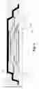
FIG. 1B is an enlargement of an alternate embodiment of corner portions 201c of the leadframe 200. In the embodiment in FIG. 1B, a notch 240 is etched, for example, half-etched, in the corner portions 201c of the leadframe 200. The notch 240 can improve engagement of the mold material 900 to the leadframe 200 and can therefore better secure the lead frame 200 to the substrate 100. It will be appreciated that while the notch 240 is described in this alternate embodiment as being etched at the corner portions 201c, the notch 240 may be formed on any other portions of the lead frame 200 to promote engagement of the mold compound 900 thereto.
FIG. 4 shows an example of a second embodiment of the semiconductor package 10 of the invention. Like-numbered elements are the same as those in the previous figures. In this embodiment, the substrate 100 has a cavity 110. Another difference is that the first semiconductor die 300 is attached to the bottom of the substrate cavity 110 via an adhesive 700.
FIG. 5 shows an example of a third embodiment of the semiconductor package 10 of the invention. Like-numbered elements are the same as those in the previous figures. Like the second embodiment, this embodiment also has a cavity 110 in the substrate 100. Another difference is that the first semiconductor die 300 is attached to the bottom of the substrate cavity 110 via solder bumps 320.
FIG. 6 shows an example of a fourth embodiment of the semiconductor package 10 of the invention. Like-numbered elements are the same as those in the previous figures. This embodiment is similar to the first embodiment except that it has an additional semiconductor die 600 attached via an adhesive 700 to the bottom surface 400b of the second semiconductor die 400. In addition, there are wire bonds 610 that electrically connect the fourth semiconductor die 600 to the intermediate portion 203 of the leadframe 200.
FIG. 7 shows an example of a fifth embodiment of the semiconductor package 10 of the invention. Like-numbered elements are the same as those in the previous figures. This embodiment is similar to the first embodiment except that only the first and second semiconductor dies 300 and 400 are shown. Additional semiconductor dies could be part of the semiconductor package 10. In addition, the top die pad surface 201a of the leadframe 200 is not exposed to the outside; rather the molding compound 900 completely covers the entire leadframe 200.
FIG. 8 shows an example of a sixth embodiment of the semiconductor package 10 of the invention. Like-numbered elements are the same as those in the previous figures. This embodiment is also similar to the first embodiment except that the third semiconductor die 500 is connected via an adhesive 700 to the substrate 100 instead of the top surface 300a of the first semiconductor die 300.
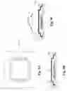
FIGS. 9A, 9B and 9C show an example of a seventh embodiment of the semiconductor package 10 of the invention. Like-numbered elements are the same as those in the previous figures. In this embodiment, the molding compound 900 encapsulates the entire top die pad surface 201a of the leadframe 200, except for a plurality of areas 260 shown in the top view of FIG. 9A. The areas 260 expose a plurality of leads. As shown in FIG. 9C, a quad flat package (QFP) 20 can be attached via leads 22 to the exposed plurality of leads 260. Likewise a quad flat no leads package (QFN) (not shown) may be attached via solder connections to the exposed plurality of leads 260.
Next, a method of assembling the inventive semiconductor package will be described in connection with FIG. 10A.
In step S1A, the second semiconductor die 400 is attached to the bottom die pad surface 201b of the lead frame 200, and at the same time in step S1B, the first semiconductor die 300 is attached to the top surface 100a of the substrate 100. Next, in step S2A, the second die 400 is wire bonded to the lead frame 200, and at the same time in step S2B, the first die 300 is wire bonded to the substrate 100. Then, in step S3, the leadframe 200 is inverted and attached to the substrate 100 at the bottom portion 205 using solder material, and thereafter the leadframe 200 and the substrate 100 are placed in a mold where mold material 900 encapsulates at least a portion of the substrate 100 and the leadframe 200. After the molding, in step S4, solder balls 800 are attached to the bottom surface 100b of the substrate 100. In step S5, the package is singulated.
Because the two die attach steps (S1A and S1B) and the two wire bonding steps (S2A and S2B) for the semiconductor dies have been combined, the assembly time decreases and the units per hour (UPH) rate increases.
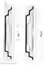
The assembly method can also be performed for a plurality of semiconductor packages. See for example, FIGS. 3A, 3B and 3C. FIG. 3A shows a cross-sectional view of a leadframe strip 200′ that includes a plurality of leadframes 200. FIG. 3A also shows a cross-sectional view of a substrate strip 100′ that includes a plurality of substrates 100 with external solder ball connections 800 formed at a bottom surface 100'b.
FIG. 3B shows a top view of the leadframe strip 200′ which shows a matrix of leadframes 200. FIG. 3C shows a top view of the substrate strip 100′ which shows a matrix of substrates 100.
During the manufacturing process, a plurality of semiconductor dies can be attached to both the leadframe strip 200′ and to the substrate strip 100′ at the same time. Next, the wire bonding step is performed for all of the semiconductor dies. Then the leadframe strip 200′ and substrate strip 100′ are attached to each other and placed in a mold where the leadframe strip 200′ and the substrate strip 100′ are encapsulated. After encapsulation, individual semiconductor packages 10 are created by singulation.
Assembling semiconductor packages in a strip form can increase both the units per hour rate and accuracy.
The invention offers several advantages over the convention packages and methods. For example, when bundling a smaller die with conductor/resistance limitations and a larger die in a semiconductor package, wire bonds for the smaller die in the semiconductor package of the present invention are kept as short as possible while the smaller die is attached to the substrate. In the conventional semiconductor package, the top smaller die will have a longer wire bond.
In the present invention, when stacking more than two dies, a “pyramid” stacking of dies on the lead frame and on the substrate can be maintained while keeping the wire bonds for the smaller dies with conductor/resistance limitations as short as possible. This can be achieved by stacking the smaller dies with conductor/resistance limitations in a pyramidal structure on the substrate and stacking the larger dies in the same manner on the leadframe. In the conventional method of die stacking, to maintain the shortest possible wire bond for the smaller dies, the dies would need to be stacked in an inverted pyramid manner on the substrate. As will be understood by persons skilled in the art, an “inverted pyramid” manner of stacking of dies would require further processing steps so that the larger top die does not sit on the bond pads of the smaller bottom die. The further processing steps may include using spacers or interposers between the dies which may result in potential package reliability issues.
As mentioned above, when the top die pad surface of the leadframe is exposed to the outside, the leadframe can act as a heat spreader that can provide increased thermal performance in both theta Ja (junction to ambient) and theta Jc (junction to case). The lead frame can also act as a shielding (i.e., electromagnetic interference shielding) when the package is assembled onto a printed circuit board (PCB).
Finally, while the various embodiments show only two dies stacked together, more dies could be added to package while maintaining the height of the package through the use of the inverted lead frame and substrate. Package thinness may further be improved by coupling the inverted lead frame to a cavity in the substrate.
While the present invention has been particularly shown and described with reference to exemplary embodiments thereof, it will be understood by those of ordinary skill in the art that various changes in form and details may be made therein without departing from the spirit and scope of the present invention as defined by the following claims.
Claims
What is claimed is:1. A semiconductor package comprising:
a substrate with a top surface and a bottom surface;
a lead frame with a top die pad surface, a bottom die pad surface and a plurality of leads, wherein the lead frame is attached to the top surface of the substrate;
a first die with a top surface and a bottom surface, wherein the bottom surface is attached to the top surface of the substrate and the first die is electrically connected to the substrate;
a second die with a top surface and a bottom surface, wherein the top surface is attached to the bottom die pad surface of the lead frame and the second die is electrically connected to the leadframe; and
an encapsulant covering at least a portion of the lead frame and substrate.
2. The package of claim 1, further comprising:
a third die with a top surface and a bottom surface, wherein the bottom surface is attached to the top surface of the substrate and the third die is electrically connected to the substrate.
3. The package of claim 2, further comprising:
a fourth die with a top surface and a bottom surface, wherein the top surface is attached to the top bottom surface of the second die and the fourth die is electrically connected to the leadframe.
4. The package of claim 1, further comprising:
a third die with a top surface and a bottom surface, wherein the bottom surface is attached to the top surface of the first die and the third die is electrically connected to the substrate.
5. The package of claim 4, further comprising:
a fourth die with a top surface and a bottom surface, wherein the top surface is attached to the bottom surface of the second die and the fourth die is electrically connected to the leadframe.
6. The package of claim 1, further comprising:
a third die with a top surface and a bottom surface, wherein the top surface is attached to the bottom surface of the second die; and
a plurality of bond wires connected between the bottom surface of the third die and the leads on the lead frame.
7. The package of claim 1, wherein the encapsulant covers the entire top die pad surface of the lead frame.
8. The package of claim 1, wherein the encapsulant covers the entire top die pad surface of the lead frame, except for a plurality of areas.
9. The package of claim 8, further comprising a second semiconductor package that is connected to the lead frame through the plurality of areas.
10. The package of claim 1, wherein the top die pad surface of the lead frame comprises an etched area and wherein the encapsulant covers the etched area, but not remaining portion of the top die pad surface.
11. A semiconductor package comprising:
a lead frame with a top die pad surface, a bottom die pad surface and a plurality of leads;
a substrate with a top surface, a bottom surface, and a cavity, wherein the lead frame is attached to the top surface of the substrate;
a first die with a top surface and a bottom surface, wherein the bottom surface is attached to the cavity of the substrate and the first die is electrically connected to the substrate;
a second die with a top surface and a bottom surface, wherein the top surface is attached to the bottom die pad surface of the lead frame and the second die is electrically connected to the leadframe; and
an encapsulant covering at least a portion of the lead frame and substrate.
12. The package of claim 11, further comprising:
a third die with a top surface and a bottom surface, wherein the bottom surface is attached to the cavity of the substrate and the third die is electrically connected to the substrate.
13. The package of claim 12, further comprising:
a fourth die with a top surface and a bottom surface, wherein the top surface is attached to the bottom surface of the second die and the fourth die is electrically connected to the leadframe.
14. The package of claim 11, further comprising:
a third die with a top surface and a bottom surface, wherein the bottom surface is attached to the top surface of the first die and the third die is electrically connected to the substrate.
15. The package of claim 14, further comprising:
a fourth die with a top surface and a bottom surface, wherein the top surface is attached to the bottom surface of the second die and the fourth die is electrically connected to the leadframe.
16. The package of claim 11, further comprising:
a third die with a top surface and a bottom surface, wherein the top surface is attached to the bottom surface of the second die and the third die is electrically connected to the lead frame.
17. The package of claim 11, wherein the encapsulant covers the entire top die pad surface of the lead frame.
18. The package of claim 11, wherein the encapsulant covers the entire top die pad surface of the lead frame, except for a plurality of areas.
19. The package of claim 18, further comprising a second semiconductor package that is connected to the lead frame through the plurality of areas.
20. The package of claim 11, wherein the top die pad surface of the lead frame comprises a half-etched area and wherein the encapsulant covers half-etched area, but not remaining portion of the top die pad surface.
21. A method of manufacturing a semiconductor package comprising:
(a) providing a substrate with a top surface and a bottom surface;
(b) providing a lead frame with a top die pad surface, a bottom die pad surface and a plurality of leads;
(c) attaching a first die with a top surface and a bottom surface to the substrate, wherein the bottom surface of the first die is attached to the top surface of the substrate and the first die is electrically connected to the substrate;
(d) attaching a second die with a top surface and a bottom surface to the lead frame, wherein the top surface of the second die is attached to the bottom die pad surface of the lead frame and the second die is electrically connected to the leadframe;
(e) attaching the lead frame to the top surface of the substrate; and
(f) encapsulating at least a portion of the lead frame and substrate.
22. The method of claim 21, further comprising:
attaching solder balls to said substrate and
singulating said semiconductor packages into individual semiconductor packages.
23. The method of claim 21, wherein steps (c) and (d) occur simultaneously.
24. A method of manufacturing a plurality of semiconductor packages comprising:
(a) providing a substrate strip with a top surface and a bottom surface,
(b) providing a lead frame strip with top die pad surfaces, bottom die pad surfaces and a plurality of leads;
(c) attaching a plurality of first dies with top surfaces and bottom surfaces to the substrate strip, wherein the bottom surfaces of the first dies are attached to the top surface of the substrate strip and the first dies are electrically connected to the substrate strip;
(d) attaching a plurality of second dies with top surfaces and bottom surfaces to the lead frame, wherein the top surfaces of the second dies are attached to the bottom die pad surfaces of the lead frame strip and the second dies are electrically connected to the leadframe strip;
(e) attaching the lead frame strip to the top surface of the substrate strip; and
(f) encapsulating at least a portion of the lead frame strip and substrate strip.
25. The method of claim 24, further comprising:
attaching solder balls to said substrate strip and
singulating said semiconductor packages into individual semiconductor packages.
26. The method of claim 24, wherein steps (c) and (d) occur simultaneously.
Images & Drawings included:


Sources:
- United States Patent and Trademark Office - verify current appl. status at the USPTO↗
Recent applications in this class:
- » 20250246514 2025-07-31
ELECTRONIC PACKAGE AND METHOD OF FORMING THE SAME - » 20250201664 2025-06-19
LIQUID METAL ENCAPSULATION DEVICE - » 20250149405 2025-05-08
SEMICONDUCTOR DEVICE, ELECTRIC POWER CONVERSION UNIT AND METHOD FOR MANUFACTURING SEMICONDUCTOR DEVICE - » 20250149404 2025-05-08
ELECTRONIC COMPONENT-INCORPORATING SUBSTRATE - » 20250079261 2025-03-06
SEMICONDUCTOR PACKAGES WITH THERMAL DISSIPATION - » 20250062188 2025-02-20
SEMICONDUCTOR PACKAGES AND MANUFACTURING METHOD OF THE SAME - » 20240363488 2024-10-31
SEMICONDUCTOR PACKAGES HAVING THERMAL CONDUCTIVE PATTERN - » 20240312868 2024-09-19
SEMICONDUCTOR DEVICE - » 20240282668 2024-08-22
PROTECTION DAM FOR A POWER MODULE WITH SPACERS - » 20240274505 2024-08-15
ELECTRONIC PACKAGE AND MANUFACTURING METHOD THEREOF
Recent applications for this Assignee:
- » 20180033759 2018-02-01
Semiconductor packages and methods of packaging semiconductor devices - » 20160211196 2016-07-21
Method of producing a semiconductor package - » 20150325511 2015-11-12
Semiconductor packages and methods of packaging semiconductor devices - » 20150102478 2015-04-16
Semiconductor packages and methods for forming semiconductor package - » 20140264835 2014-09-18
Semiconductor packages and methods of packaging semiconductor devices - » 20140264792 2014-09-18
Semiconductor packages and methods of packaging semiconductor devices - » 20140264789 2014-09-18
Semiconductor packages and methods of packaging semiconductor devices - » 20140227832 2014-08-14
Semiconductor packages and methods of packaging semiconductor devices - » 20140225242 2014-08-14
Semiconductor packages and methods of packaging semiconductor devices - » 20140138808 2014-05-22
Leadframe area array packaging technology