ELECTRIC CIRCUIT PACKAGE
US20080192449A1
2008-08-14
12/028,864
2008-02-11
Abstract:
An electric circuit package includes: a printed circuit substrate having an insulating layer and conductive pattern layers formed on an upper surface of the insulating layer; at least one of electronic parts disposed on an upper surface of the printed circuit substrate; at least one of conductive pins electrically connected to an conductive pattern layer providing grounding among the conductive pattern layers; and a molding member formed on the insulating layer in such a manner that the conductive pins and the electric parts are buried in the molding member, wherein each conductive pin has an upper surface exposed to an upper part of the molding member.
Inventors:
- Kyu-Sub Kwak 16 🇰🇷 Seoul, South Korea
- Shi-Yun CHO 53 🇰🇷 Anyang-si, South Korea
- Seung-Woo Han 22 🇰🇷 Seoul, South Korea
- Kyung-wan PARK 29 🇰🇷 Suwon-si, South Korea
- Dong-Churl KIM 10 🇰🇷 Ansan-si, South Korea
- Hong-Kweun KIM 8 🇰🇷 Ansan-si, South Korea
Interested in similar patents?
Get notified when new applications in this technology area are published.
Classification:
H01L2924/00014 » CPC further
Indexing scheme for arrangements or methods for connecting or disconnecting semiconductor or solid-state bodies as covered by; Technical content checked by a classifier the subject-matter covered by the group, the symbol of which is combined with the symbol of this group, being disclosed without further technical details
H05K9/0022 » CPC main
Screening of apparatus or components against electric or magnetic fields; Casings with localised screening of components mounted on printed circuit boards [PCB]
H05K9/0022 » CPC main
Screening of apparatus or components against electric or magnetic fields; Casings with localised screening of components mounted on printed circuit boards [PCB]
H01L23/3121 » CPC further
Details of semiconductor or other solid state devices; Encapsulations, e.g. encapsulating layers, coatings, e.g. for protection characterised by the arrangement or shape the device being completely enclosed a substrate forming part of the encapsulation
H01L23/49811 » CPC further
Details of semiconductor or other solid state devices; Arrangements for conducting electric current to or from the solid state body in operation, e.g. leads, terminal arrangements ; Selection of materials therefor consisting of soldered constructions; Leads, on insulating substrates, Additional leads joined to the metallisation on the insulating substrate, e.g. pins, bumps, wires, flat leads
H01L23/50 » CPC further
Details of semiconductor or other solid state devices; Arrangements for conducting electric current to or from the solid state body in operation, e.g. leads, terminal arrangements ; Selection of materials therefor for integrated circuit devices, e.g. power bus, number of leads
H05K1/0218 » CPC further
Printed circuits; Details; Electrical arrangements not otherwise provided for; Reduction of cross-talk, noise or electromagnetic interference by printed shielding conductors, ground planes or power plane
H05K1/0218 » CPC further
Printed circuits; Details; Electrical arrangements not otherwise provided for; Reduction of cross-talk, noise or electromagnetic interference by printed shielding conductors, ground planes or power plane
H01L2924/3025 » CPC further
Indexing scheme for arrangements or methods for connecting or disconnecting semiconductor or solid-state bodies as covered by; Technical effects; Electrical effects Electromagnetic shielding
H05K3/284 » CPC further
Apparatus or processes for manufacturing printed circuits; Secondary treatment of printed circuits; Applying non-metallic protective coatings for encapsulating mounted components
H05K3/284 » CPC further
Apparatus or processes for manufacturing printed circuits; Secondary treatment of printed circuits; Applying non-metallic protective coatings for encapsulating mounted components
H05K2201/10318 » CPC further
Indexing scheme relating to printed circuits covered by; Details of components or other objects attached to or integrated in a printed circuit board; Other objects, e.g. metallic pieces; Surface mounted metallic connector elements Surface mounted metallic pins
H05K2201/10318 » CPC further
Indexing scheme relating to printed circuits covered by; Details of components or other objects attached to or integrated in a printed circuit board; Other objects, e.g. metallic pieces; Surface mounted metallic connector elements Surface mounted metallic pins
H05K2203/1316 » CPC further
Indexing scheme relating to apparatus or processes for manufacturing printed circuits covered by; Moulding and encapsulation; Deposition techniques; Protective layers; Moulding and encapsulation Moulded encapsulation of mounted components
H05K2203/1316 » CPC further
Indexing scheme relating to apparatus or processes for manufacturing printed circuits covered by; Moulding and encapsulation; Deposition techniques; Protective layers; Moulding and encapsulation Moulded encapsulation of mounted components
H01L2924/00011 » CPC further
Indexing scheme for arrangements or methods for connecting or disconnecting semiconductor or solid-state bodies as covered by; Technical content checked by a classifier Not relevant to the scope of the group, the symbol of which is combined with the symbol of this group
H01L2224/0401 » CPC further
Indexing scheme for arrangements for connecting or disconnecting semiconductor or solid-state bodies and methods related thereto as covered by; Means for bonding being attached to, or being formed on, the surface to be connected, e.g. chip-to-package, die-attach, "first-level" interconnects; Manufacturing methods related thereto; Bonding areas; Manufacturing methods related thereto; Structure, shape, material or disposition of the bonding areas prior to the connecting process Bonding areas specifically adapted for bump connectors, e.g. under bump metallisation [UBM]
H05K7/00 IPC
Constructional details common to different types of electric apparatus
H05K7/00 IPC
Constructional details common to different types of electric apparatus
Description
CLAIM OF PRIORITY
This application claims priority to an application entitled “Electric circuit package,” filed in the Korean Intellectual Property Office on Feb. 12, 2007 and assigned Serial No. 2007-14368, the contents of which are hereby incorporated by reference.
BACKGROUND OF THE INVENTION
1. Field of the Invention
The present invention relates to an electric circuit package in which a plurality of electric devices are integrated therein, and more particularly to an electric circuit package having an electromagnetic wave shielding means.
2. Description of the Related Art
An electric circuit package is a System in Package (SiP) structure having a plurality of electric parts integrated therein. Particularly, when a device generating many electromagnetic waves, such as a radio frequency integrated circuit (RFIC), is included therein, the electric circuit package needs an electromagnetic wave shielding means.
The electromagnetic shielding means can use a metallic can surrounding an exterior of a module. A structure that electric parts are mounted in the metallic can has been proposed. However, this type of conventional electric circuit packages is used to restrain electromagnetic waves from escaping outside or flowing inside, but it is difficult to shield electromagnetic waves generated in interior devices. Furthermore, when a metallic can for shielding electromagnetic waves is included in the conventional electric circuit package, it is limited to employ the metallic can in a magnified printed circuit substrate.
SUMMARY OF THE INVENTION
Accordingly, the present invention has been made to solve the above-mentioned problems occurring in the prior art and provides additional advantages, by providing an electric circuit package which can minimize high-integration and generation of electromagnetic wave interference between respective devices.
In accordance with an aspect of the present invention, an electric circuit package includes: a printed circuit substrate having an insulating layer and conductive pattern layers formed on an upper surface of the insulating layer; at least one of electronic parts disposed on an upper surface of the printed circuit substrate; at least one of conductive pins electrically coupled to an conductive pattern layer providing grounding among the conductive pattern layers; and a molding member formed on the insulating layer in such a manner that the conductive pins and the electric parts are buried in the molding member, wherein each conductive pin has an upper surface exposed to an upper part of the molding member.
BRIEF DESCRIPTION OF THE DRAWINGS
The above and other aspects, features and advantages of the present invention will be more apparent from the following detailed description taken in conjunction with the accompanying drawings, in which:
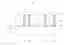
FIG. 1 is a sectional view illustrating an electric circuit package according to an exemplary embodiment of the present invention.
DETAILED DESCRIPTION OF THE INVENTION
Hereinafter, exemplary embodiments of the present invention will be described with reference to the accompanying drawings. For the purposes of clarity and simplicity, a detailed description of known functions and configurations incorporated herein will be omitted when it may make the subject matter of the present invention unclear.
FIG. 1 is a sectional view illustrating an electric circuit package according to an exemplary embodiment of the present invention. As shown, an electric circuit package 100 according to the present embodiment includes a printed circuit substrate 110, electric parts 140 and 150 disposed on an upper surface of the printed circuit substrate 110, at least one conductive pin 121, a molding member 160 having the conductive pins 121 and the electric parts 140 and 150 buried therein, and a conductive plate 130.
The printed circuit substrate 110 includes an insulating layer 111 such as a core, and conductive pattern layers 112a and 112b formed by etching plates of conductive metallic material, such as Cu, formed on the insulating layer 111. The electric parts 140 and 150 are disposed on the upper surface of the printed circuit substrate 110, and can be electrically connected to the conductive pattern layers 112a and 112b by soldering or wiring, etc.
The conductive pattern layers 112a and 112b provide circuit wirings of electric parts to be integrated, and may include circuit wirings 112a for providing a power or a signal and data process, and ground wiring 112b for grounding.
The conductive pins 121 can be electrically connected to the ground wiring 112b, among the conductive pattern layers 112a and 112b, to be grounded thereto, and can include conductive material such as metal. Furthermore, each of the conductive pins 121 may be a rod having a circular or polygonal section with respect to its longer axis, and may surround a device requiring electromagnetic wave shielding.
The conductive pins 121 have opposite ends on which solders 122a and 122b are applied, respectively, so that the conductive pins 121 can be electrically connected to the grounding wirings 112b, or to the conductive plate 130. Further, each conductive pin 121 has a height higher than the electric parts 140 and 150, and can be disposed between the electric parts 140 and 150 in such a manner that the conductive pins 121 surround the electric parts 140 and 150.
The molding member 160 can be formed on the insulation layer 160 by using an epoxy molding in such a manner that the conductive pins 121 and the electric parts 140 and 150 are buried therein. The molding member 160 tightly surrounds the conductive pins 121, thereby fixedly holding the conductive pins. Additionally, the molding member 160 covers the electric parts 140 and 150, thereby shielding electromagnetic waves.
However, each conductive pin 121 has an upper surface exposed to an upper part of the molding member 160. The conductive plate 130 is disposed on the molding member 160 so as to enable the conductive pins 121 to be electrically connected to each other. The conductive plate 130 can be electrically and physically connected to the conductive pins 121 through a process, such as a reflow process.
The present invention includes a plurality of the grounded conductive pins and the molding member in which the conductive pins and the electric parts are buried, thereby providing the electric circuit package which can minimize electromagnetic wave interference despite its minimized volume.
While the invention has been shown and described with reference to certain exemplary embodiments thereof, it will be understood by those skilled in the art that various changes in form and details may be made therein without departing from the spirit and scope of the invention as defined by the appended claims.
Claims
What is claimed is:1. An electric circuit package comprising:
a printed circuit substrate having an insulating layer and conductive pattern layers formed on an upper surface of the insulating layer;
at least one of electronic parts disposed on an upper surface of the printed circuit substrate;
at least one of conductive pins electrically coupled to an conductive pattern layer to provide grounding among the conductive pattern layers; and
a molding member formed on the insulating layer in such a manner that the conductive pins and the electric parts are buried in the molding member, wherein each conductive pin has an upper surface exposed to an upper part of the molding member.
2. The electric circuit package as claimed in claim 1, further comprising a conductive plate disposed on an upper surface of the molding member in such a manner that the conductive plate is electrically coupled to the conductive pins.
3. The electric circuit package as claimed in claim 1, wherein each conductive pin has a height higher than the electric parts.
4. The electric circuit package as claimed in claim 1, wherein each conductive pin is coupled to the conductive plate and the corresponding conductive pattern layer by solders applied on an upper surface and a lower surface of each conductive pin.
5. The electric circuit package as claimed in claim 1, wherein the conductive pins are disposed between the electric parts.
6. The electric circuit package as claimed in claim 1, wherein the conductive pins are arranged so as to surround the electric parts.
7. The electric circuit package as claimed in claim 1, wherein the electric parts are electrically coupled to the conductive pattern layers by soldering or wiring process.
8. The electric circuit package as claimed in claim 1, wherein each of the conductive pins comprises a rod having a circular or polygonal section with respect to its longer axis.
9. The electric circuit package as claimed in claim 1, wherein each of the conductive pins surrounds a device requiring electromagnetic wave shielding.
10. The electric circuit package as claimed in claim 1, wherein the molding member is formed on the insulation layer using an epoxy molding.
Images & Drawings included:
Sources:
- United States Patent and Trademark Office - verify current appl. status at the USPTO↗
Similar patent applications:
- » 20140015132
Systems and methods for mitigation of mechanical degradation in high performance electrical circuit packages - » 20080080141
Electrical Circuit Package - » 20060237844
Semiconductor integrated circuit package having electrically disconnected solder balls for mounting - » 20080142950
Semiconductor integrated circuit package having electrically disconnected solder balls for mounting - » 20050026327
Semiconductor integrated circuit package having electrically disconnected solder balls for mounting - » 20060237845
Semiconductor integrated circuit package having electrically disconnected solder balls for mounting - » 20120045870
Method of manufacturing leadless integrated circuit packages having electrically routed contacts - » 20100224971
Leadless integrated circuit package having electrically routed contacts - » 20130288432
Method of manufacturing leadless integrated circuit packages having electrically routed contacts - » 20210041649
Integrated circuit packages having electrical and optical connectivity and methods of making the same
Recent applications in this class:
- » 20240260242 2024-08-01
ANTI-MAGNETIC INTERFERENCE COMPONENT AND ELECTRONIC DEVICE - » 20240188262 2024-06-06
BUILDING CONTROLLER WITH LATERAL SIDE SHIELDING - » 20230380120 2023-11-23
RADIO FREQUENCY MODULE AND COMMUNICATION DEVICE - » 20230371219 2023-11-16
MODULE - » 20230345685 2023-10-26
INTEGRATED DEVICE PACKAGE WITH REDUCED THICKNESS - » 20230345684 2023-10-26
ELECTROMAGNETIC INTERFERENCE (EMI) SHIELDED INTEGRATED DEVICE PACKAGE - » 20230209789 2023-06-29
MODULE AND ELECTRONIC COMPONENT - » 20230209788 2023-06-29
MODULE AND METHOD FOR MANUFACTURING MODULE - » 20230200032 2023-06-22
MODULE - » 20230189490 2023-06-15
Module