Packaging substrate and method for manufacturing the same
US20080257595A1
2008-10-23
12/081,423
2008-04-16
Abstract:
The present invention relates to a packaging substrate and a method for manufacturing the same. The packaging substrate includes: a substrate body, having a plurality of conductive pads on the surface thereof, wherein the top surfaces of the conductive pads have a concave each; a solder mask, disposed on the surface of the substrate body and having a plurality of openings to correspondingly expose the concaves of the conductive pads each; and a plurality of metal bumps, disposed correspondingly in the openings of the solder mask and over the concaves of the conductive pads. The present invention increases the joint surface area between the metal bumps and the conductive pads so as to inhibit the joint crack and improve the reliability of the conductive structure of the packaging substrate.
Assignee:
- PHOENIX PRECISION TECHNOLOGY CORPORATION 52 🇹🇼 Hsinchu, Taiwan
Interested in similar patents?
Get notified when new applications in this technology area are published.
Classification:
H05K3/4007 » CPC main
Apparatus or processes for manufacturing printed circuits; Forming printed elements for providing electric connections to or between printed circuits Surface contacts, e.g. bumps
H05K3/4007 » CPC main
Apparatus or processes for manufacturing printed circuits; Forming printed elements for providing electric connections to or between printed circuits Surface contacts, e.g. bumps
H01L23/49816 » CPC further
Details of semiconductor or other solid state devices; Arrangements for conducting electric current to or from the solid state body in operation, e.g. leads, terminal arrangements ; Selection of materials therefor consisting of soldered constructions; Leads, on insulating substrates,; Additional leads joined to the metallisation on the insulating substrate, e.g. pins, bumps, wires, flat leads Spherical bumps on the substrate for external connection, e.g. ball grid arrays [BGA]
H01L24/11 » CPC further
Arrangements for connecting or disconnecting semiconductor or solid-state bodies; Methods or apparatus related thereto; Means for bonding being attached to, or being formed on, the surface to be connected, e.g. chip-to-package, die-attach, "first-level" interconnects; Manufacturing methods related thereto; Bump connectors ; Manufacturing methods related thereto Manufacturing methods
H01L2224/05001 » CPC further
Indexing scheme for arrangements for connecting or disconnecting semiconductor or solid-state bodies and methods related thereto as covered by; Means for bonding being attached to, or being formed on, the surface to be connected, e.g. chip-to-package, die-attach, "first-level" interconnects; Manufacturing methods related thereto; Bonding areas; Manufacturing methods related thereto; Structure, shape, material or disposition of the bonding areas prior to the connecting process of an individual bonding area Internal layers
H01R12/57 » CPC further
Structural associations of a plurality of mutually-insulated electrical connecting elements, specially adapted for printed circuits, e.g. printed circuit boards [PCBs], flat or ribbon cables, or like generally planar structures, e.g. terminal strips, terminal blocks; Coupling devices specially adapted for printed circuits, flat or ribbon cables, or like generally planar structures; Terminals specially adapted for contact with, or insertion into, printed circuits, flat or ribbon cables, or like generally planar structures; Fixed connections for rigid printed circuits or like structures characterised by the terminals surface mounting terminals
H05K3/06 » CPC further
Apparatus or processes for manufacturing printed circuits in which the conductive material is applied to the surface of the insulating support and is thereafter removed from such areas of the surface which are not intended for current conducting or shielding the conductive material being removed chemically or electrolytically, e.g. by photo-etch process
H05K3/243 » CPC further
Apparatus or processes for manufacturing printed circuits; Secondary treatment of printed circuits; Reinforcing the conductive pattern characterised by selective plating, e.g. for finish plating of pads
H05K3/243 » CPC further
Apparatus or processes for manufacturing printed circuits; Secondary treatment of printed circuits; Reinforcing the conductive pattern characterised by selective plating, e.g. for finish plating of pads
H05K3/28 » CPC further
Apparatus or processes for manufacturing printed circuits; Secondary treatment of printed circuits Applying non-metallic protective coatings
H05K3/28 » CPC further
Apparatus or processes for manufacturing printed circuits; Secondary treatment of printed circuits Applying non-metallic protective coatings
H05K2201/0367 » CPC further
Indexing scheme relating to printed circuits covered by; Conductive materials; Structure of the conductor; Conductor shape Metallic bump or raised conductor not used as solder bump
H05K2201/0367 » CPC further
Indexing scheme relating to printed circuits covered by; Conductive materials; Structure of the conductor; Conductor shape Metallic bump or raised conductor not used as solder bump
H05K2201/09436 » CPC further
Indexing scheme relating to printed circuits covered by; Shape and layout; Shape and layout details of conductors; Pads and lands Pads or lands on permanent coating which covers the other conductors
H05K2201/09436 » CPC further
Indexing scheme relating to printed circuits covered by; Shape and layout; Shape and layout details of conductors; Pads and lands Pads or lands on permanent coating which covers the other conductors
H05K2201/09745 » CPC further
Indexing scheme relating to printed circuits covered by; Shape and layout; Shape and layout details of conductors covering at least two types of conductors provided for in - Recess in conductor, e.g. in pad or in metallic substrate
H05K2201/09745 » CPC further
Indexing scheme relating to printed circuits covered by; Shape and layout; Shape and layout details of conductors covering at least two types of conductors provided for in - Recess in conductor, e.g. in pad or in metallic substrate
H05K2203/0353 » CPC further
Indexing scheme relating to apparatus or processes for manufacturing printed circuits covered by; Metal processing Making conductive layer thin, e.g. by etching
H05K2203/0353 » CPC further
Indexing scheme relating to apparatus or processes for manufacturing printed circuits covered by; Metal processing Making conductive layer thin, e.g. by etching
Y10T29/49155 » CPC further
Metal working; Method of mechanical manufacture; Electrical device making; Conductor or circuit manufacturing; On flat or curved insulated base, e.g., printed circuit, etc. Manufacturing circuit on or in base
H01L2924/14 » CPC further
Indexing scheme for arrangements or methods for connecting or disconnecting semiconductor or solid-state bodies as covered by; Details of semiconductor or other solid state devices to be connected; Device type Integrated circuits
H01L2924/00 » CPC further
Indexing scheme for arrangements or methods for connecting or disconnecting semiconductor or solid-state bodies as covered by
H01L2924/00014 » CPC further
Indexing scheme for arrangements or methods for connecting or disconnecting semiconductor or solid-state bodies as covered by; Technical content checked by a classifier the subject-matter covered by the group, the symbol of which is combined with the symbol of this group, being disclosed without further technical details
H05K3/10 IPC
Apparatus or processes for manufacturing printed circuits in which conductive material is applied to the insulating support in such a manner as to form the desired conductive pattern
H05K3/10 IPC
Apparatus or processes for manufacturing printed circuits in which conductive material is applied to the insulating support in such a manner as to form the desired conductive pattern
H01L2924/01024 » CPC further
Indexing scheme for arrangements or methods for connecting or disconnecting semiconductor or solid-state bodies as covered by; Chemical elements Chromium [Cr]
H01L2924/01082 » CPC further
Indexing scheme for arrangements or methods for connecting or disconnecting semiconductor or solid-state bodies as covered by; Chemical elements Lead [Pb]
H01L2924/01022 » CPC further
Indexing scheme for arrangements or methods for connecting or disconnecting semiconductor or solid-state bodies as covered by; Chemical elements Titanium [Ti]
H01L2924/01046 » CPC further
Indexing scheme for arrangements or methods for connecting or disconnecting semiconductor or solid-state bodies as covered by; Chemical elements Palladium [Pd]
H01L2924/01079 » CPC further
Indexing scheme for arrangements or methods for connecting or disconnecting semiconductor or solid-state bodies as covered by; Chemical elements Gold [Au]
Description
BACKGROUND OF THE INVENTION
1. Field of the Invention
The present invention relates to a packaging substrate and a method for manufacturing the same and, more particularly, to a packaging substrate that can increase the joint surface area between conductive pads and metal bumps and a method for manufacturing the same.
2. Description of Related Art
As the electronic industry develops rapidly, research accordingly moves towards electronic devices with multifunction and high efficiency. Hence, circuit boards with many active and passive components and circuit connections have advanced from being single-layered boards to multiple-layered boards so that the packaging requirements such as integration and miniaturization in semiconductor packaging can be met. Furthermore, interlayer connection technique is also applied in this field to expand circuit layout space in a limited circuit board and to meet the demand of the application of high-density integrated circuits.
In a general process for manufacturing semiconductor devices, semiconductor chip carriers such as substrates or lead frames suitable for semiconductor devices are first provided by manufacturers. Then, the semiconductor chip carriers are processed by semiconductor chip attachment, wire bonding, encapsulating, implanting solder ball etc. for assembling semiconductor devices. In general, a conventional semiconductor package structure is made such that a semiconductor chip is mounted by its back surface on the top surface of the substrate, then the package structure is finished through wire bonding, or a semiconductor chip is mounted by the active surface thereof on the top surface of the substrate, thereby finishing a flip-chip package structure, followed by placing solder balls on the back surface of the substrate to provide electrical connections for an electronic device like a printed circuit board.
In the aforementioned flip chip package, when the line width and the space width of the semiconductor packaging substrate are reduced, the decrease of joint surface area causes the reduction of joint strength. Thereby, the reduced joint strength cannot always bear the stress between the chip and the substrate, and the matter of joint crack becomes serious.
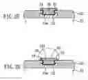
With reference to FIGS. 1A and 1B, there is shown a conventional packaging substrate. As shown in FIG. 1A, the conventional packaging substrate comprises: a substrate body 11 having a plurality of conductive pads 12 on the surface thereof; a solder mask 13 disposed on the surface of the substrate body 11 and having a plurality of openings to correspondingly expose the conductive pads 12; and metal bumps 14 formed correspondingly in the openings. Hereafter, the process for forming the metal bumps 14 is illustrated. First, a seed layer (not shown in the figures) is formed on the surface of the substrate body 11, and then a patterned photoresist layer (not shown in the figures) having openings to correspondingly expose the conductive pads 12 is formed. Subsequently, metal bumps 14 are formed correspondingly in the openings by electroplating. Herein, the material of the metal bumps 14 can be copper or other metals. Finally, the photoresist layer and the seed layer covered thereby are removed. In addition, as shown in FIG. 1B, solder bumps 15 can be formed on the surfaces of the metal bumps 14 to electrically connect with a chip (not shown in the figures) by reflow soldering.
Although the aforementioned structure can be used to electrically connect with a chip, it falls short of demand for package structure with high-density integration and miniaturization, owing to the trend of reducing the critical dimension (such as minimum line width), such that the reduced joint surface area between the metal bumps 14 and the conductive pads 12 makes the joint strength fail to bear the stress between the chip and the substrate, thereby the matter of joint crack frequently occurs and the reliability requirement of the product cannot be met.
SUMMARY OF THE INVENTION
In view of the above-mentioned disadvantages, the object of the present invention is to provide a packaging substrate to increase the joint surface area between metal bumps and conductive pads and further inhibit the joint crack generally occurring in a conventional packaging substrate. Accordingly, the reliability of the packaging substrate can be enhanced, and the packaging substrate can be employed for meeting the trend of reducing the critical dimension of circuits of the substrate.
To achieve the aforementioned and other objects, the present invention provides a packaging substrate comprising: a substrate body, having a plurality of conductive pads on the surface thereof, wherein the top surfaces of the conductive pads have a concave each; a solder mask, disposed on the surface of the substrate body and having a plurality of openings to correspondingly expose the concaves of the conductive pads; and a plurality of metal bumps, disposed correspondingly in the openings of the solder mask and over the concaves of the conductive pads. Herein, the metal bumps can be higher than the surface of the solder mask, and the parts of metal bumps higher than the surface of the solder mask can have a width bigger than the size of the openings of the solder mask.
The packaging substrate of the present invention can further comprise solder bumps correspondingly disposed over the surfaces of the metal bumps.
The aforementioned packaging substrate of the present invention can further comprise a metal connective layer disposed between the metal bumps and the solder bumps.
The present invention further provides a method for manufacturing a packaging substrate, for example but not limited thereto, comprising: providing a substrate body, which has a plurality of conductive pads on the surface thereof; forming a solder mask on the surface of the substrate body, and forming a plurality of openings in the solder mask to correspondingly expose the conductive pads; micro-etching the surfaces of the conductive pads to form concaves; and forming metal bumps by electroplating correspondingly in the openings of the solder mask.
The aforementioned method can further comprise a step for forming solder bumps over the surfaces of the metal bumps.
The aforementioned method can further comprise a step for forming a metal connective layer on the surfaces of the metal bumps before forming the solder bumps.
In the present invention, the metal bumps are formed over the concaves of the conductive pads to increase the joint surface area and further enhance the connection between the metal bumps and the conductive pads, so that the joint crack generally occurring in a conventional packaging substrate can be inhibited so as to enhance the reliability of the packaging substrate. Accordingly, the packaging substrate of the present invention can be employed for meeting the trend of reducing the critical dimension of circuits of the substrate.
Other objects, advantages, and novel features of the invention will become more apparent from the following detailed description when taken in conjunction with the accompanying drawings.
BRIEF DESCRIPTION OF THE DRAWINGS
FIGS. 1A and 1B show cross-sectional views of conventional packaging substrate; and
FIGS. 2A to 2G show a process for manufacturing a packaging substrate of a preferred embodiment of the present invention.
DETAILED DESCRIPTION OF THE PREFERRED EMBODIMENT
Because the specific embodiments illustrate the practice of the present invention, a person having ordinary skill in the art can easily understand other advantages and efficiency of the present invention through the content disclosed therein. The present invention can also be practiced or applied by other variant embodiments. Many other possible modifications and variations of any detail in the present specification based on different outlooks and applications can be made without departing from the spirit of the invention.
Method Embodiment
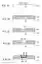
With reference to FIG. 2A, a substrate body 21 is first provided, which has a plurality of conductive pads 22 on the surface thereof. Herein, the material of the conductive pads 22 can be selected from the group consisting of copper, tin, nickel, chromium, titanium, copper-chromium alloy and tin-lead alloy. In the present embodiment, the material of the conductive pads 22 is copper. With reference to FIGS. 2B and 2C, a solder mask 23 is formed on the surface of the substrate body 21, and a plurality of openings 231 are formed in the solder mask 23 to correspondingly expose the conductive pads 22. With reference to FIG. 2D, after the openings 231 of the solder mask 23 are formed, concaves 22a are formed on the surfaces of the conductive pads 22 by a micro-etching process. Herein, the micro-etching process is a wet etching process. Subsequently, as shown in FIG. 2E, metal bumps 26 are formed correspondingly in the openings 231 (as shown in FIG. 2D) of the solder mask 23 by electroplating. As shown in FIG. 2E, the metal bumps are formed over the concaves 22a of the conductive pads 22. The material of the metal bumps 22 can be selected from the group consisting of copper, tin, nickel, chromium, titanium, copper-chromium alloy and tin-lead alloy. In the present embodiment, the material of the metal bumps is copper.
In the above-mentioned method, the process for forming the metal bumps 26 comprises the following steps. First, a seed layer 24 is formed on the surface of the substrate body 21 to function as a current conduction path needed for a following electroplating process. Then, a photoresist layer (not shown in the figures) is formed on the surface of the seed layer 24, and a plurality of openings (not shown in the figures) are formed in the photoresist layer. Herein, the openings of the photoresist layer correspond to the openings of the solder mask 23. Subsequently, metal bumps 26 are formed in the openings of the photoresist layer and the openings of the solder mask 23 and over the concaves 22a of the conductive pads 22. Finally, the photoresist layer and the seed layer 24 covered thereby are removed. Herein, the material of the seed layer 24 can be selected from the group consisting of copper, tin, nickel, chromium, titanium, copper-chromium alloy and tin-lead alloy, and the seed layer 24 can be formed by physical deposition (such as sputtering or evaporation) or chemical deposition (such as electroless plating). In the present embodiment, the material of the seed layer 24 is copper, and the seed layer 24 is formed by electroless plating.
Subsequently, as shown in FIG. 2F, a metal connective layer 27 is formed on the surface of the metal bumps 26 by physical deposition (such as sputtering or evaporation) or chemical deposition (such as electroless plating). The material of the metal connective layer 27 can be selected from the group consisting of tin, silver, nickel, gold, chromium/titanium, nickel/gold, nickel/palladium and nickel/palladium/gold. In the present embodiment, an electroless plating process is performed to deposit a nickel layer on the surfaces of the metal bumps 26 and then a gold layer on the surface of the nickel layer.
Finally, as shown in FIG. 2G, solder bumps 28 are formed by electroplating or printing.
Structure Embodiment
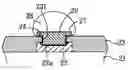
As shown in FIG. 2G, the packaging substrate of the present embodiment comprises: a substrate body 21, having a plurality of conductive pads 22 on the surface thereof, wherein the top surfaces of the conductive pads 22 have a concave 22a each; a solder mask 23, disposed on the surface of the substrate body 21 and having a plurality of openings 231 to correspondingly expose the concaves 22a of the conductive pads 22; and a plurality of metal bumps 26, disposed correspondingly in the openings 231 of the solder mask 23 and over the concaves 22a of the conductive pads 22. Herein, the metal bumps 26 are higher than the surface of the solder mask 23, and the parts of metal bumps 26 higher than the surface of the solder mask 23 have a width bigger than the size of the openings 231 of the solder mask 23. Also, the parts of metal bumps 26 higher than the surface of the solder mask 23 can have a width equal to the size of the openings 231 of the solder mask 23 (not shown in the figures).
In the above-illustrated structure, the packaging substrate further comprises solder bumps 28 correspondingly disposed over the surfaces of the metal bumps 26.
In the above-illustrated structure, the packaging substrate further comprises a metal connective layer 27 disposed between the metal bumps 26 and the solder bumps 28.
In the above-illustrated structure, the material of the metal connective layer 27 is selected from the group consisting of tin, silver, nickel, gold, chromium/titanium, nickel/gold, nickel/palladium, and nickel/palladium/gold.
In the above-illustrated structure, the material of the metal bumps 26 is selected from the group consisting of copper, tin, nickel, chromium, titanium, copper-chromium alloy, and tin-lead alloy.
As above-mentioned, in the packaging substrate and the method for manufacturing the same, the metal bumps are formed over the concaves of the conductive pads to increase the joint surface area and further enhance the connection between the metal bumps and the conductive pads, so that the joint crack between the metal bumps and the conductive pads can be inhibited so as to enhance the reliability of the packaging substrate. Accordingly, the packaging substrate of the present invention can be employed for meeting the trend of reducing the critical dimension of circuits of the substrate.
Although the present invention has been explained in relation to its preferred embodiment, it is to be understood that many other possible modifications and variations can be made without departing from the scope of the invention as hereinafter claimed.
Claims
What is claimed is:1. A packaging substrate, comprising:
a substrate body, having a plurality of conductive pads on the surface thereof, wherein the top surfaces of the conductive pads have a concave each;
a solder mask, disposed on the surface of the substrate body and having a plurality of openings to correspondingly expose the concaves of the conductive pads; and
a plurality of metal bumps, correspondingly disposed in the openings of the solder mask and over the concaves of the conductive pads.
2. The packaging substrate as claimed in claim 1, wherein the metal bumps are higher than the surface of the solder mask, and the parts of metal bumps higher than the surface of the solder mask have a width bigger than the size of the openings of the solder mask.
3. The packaging substrate as claimed in claim 1, further comprising solder bumps correspondingly disposed over the surfaces of the metal bumps.
4. The packaging substrate as claimed in claim 3, further comprising a metal connective layer disposed between the metal bumps and the solder bumps.
5. The packaging substrate as claimed in claim 4, wherein the material of the metal connective layer is selected from the group consisting of tin, silver, nickel, gold, chromium/titanium, nickel/gold, nickel/palladium, and nickel/palladium/gold.
6. The packaging substrate as claimed in claim 1, wherein the material of the metal bumps is selected from the group consisting of copper, tin, nickel, chromium, titanium, copper-chromium alloy, and tin-lead alloy.
7. A method for manufacturing a packaging substrate, comprising:
providing a substrate body, which has a plurality of conductive pads on the surface thereof;
forming a solder mask on the surface of the substrate body, and forming a plurality of openings in the solder mask to correspondingly expose the conductive pads;
micro-etching the surfaces of the conductive pads to form concaves; and
forming metal bumps by electroplating correspondingly in the openings of the solder mask.
8. The method as claimed in claim 7, wherein the metal bumps are formed by a process comprising:
forming a seed layer on the surface of the substrate body;
forming a photoresist layer on the surface of the seed layer and forming a plurality of openings in the photoresist layer, wherein the openings of the photoresist layer correspond to the openings of the solder mask;
forming metal bumps by electroplating correspondingly in the openings of the photoresist layer and the openings of the solder mask and over the concaves of the conductive pads exposed therein; and
removing the photoresist layer and the seed layer covered thereby.
9. The method as claimed in claim 7, further comprising forming solder bumps correspondingly over the surfaces of the metal bumps each.
10. The method as claimed in claim 9, wherein the solder bumps are formed by electroplating or printing.
11. The method as claimed in claim 9, further comprising forming a metal connective layer correspondingly on the surfaces of the metal bumps before forming the solder bumps.
12. The method as claimed in claim 11, wherein the metal connective layer is formed by physical deposition or chemical deposition.
Images & Drawings included:
Sources:
- United States Patent and Trademark Office - verify current appl. status at the USPTO↗
Similar patent applications:
- » 20210118790
Package substrate and method of manufacturing the package substrate, and semiconductor package including the package substrate and method of manufacturing the semiconductor package - » 20250149400
PACKAGING SUBSTRATE AND MANUFACTURING METHOD OF PACKAGING SUBSTRATE - » 20250140669
PACKAGING SUBSTRATE AND MANUFACTURING METHOD OF PACKAGING SUBSTRATE - » 20250174538
PACKAGING SUBSTRATE AND MANUFACTURING METHOD OF PACKAGING SUBSTRATE - » 20180151408
Glass substrate, laminated substrate, laminated substrate manufacturing method, laminate, package, and glass substrate manufacturing method - » 20250140707
PACKAGING SUBSTRATE AND MANUFACTURING METHOD OF PACKAGING SUBSTRATE - » 20210366760
GLASS SUBSTRATE, LAMINATED SUBSTRATE, LAMINATED SUBSTRATE MANUFACTURING METHOD, LAMINATE, PACKAGE, AND GLASS SUBSTRATE MANUFACTURING METHOD - » 20160293416
Manufacturing method of package substrate and package manufacturing method of semiconductor device - » 20250112098
PACKAGING SUBSTRATE, METHOD OF MANUFACTURING AN ELEMENT PACKAGE AND METHOD OF MANUFACTURING PACKAGING SUBSTRATE - » 20150054162
METHOD OF MANUFACTURING CHIP PACKAGE SUBSTRATE AND METHOD OF MANUFACTURING CHIP PACKAGE
Recent applications in this class:
- » 20250126722 2025-04-17
CIRCUIT COMPENSATION METHOD APPLIED TO PATTERN DISPLACEMENT AND CIRCUIT STRUCTURE - » 20250107008 2025-03-27
PRINTED CIRCUIT BOARD - » 20250098076 2025-03-20
BOARD AND ELECTRONIC DEVICE - » 20240188224 2024-06-06
Electrical devices with electrodes on softening polymers and methods of manufacturing thereof - » 20240164026 2024-05-16
PRINTED CIRCUIT BOARD - » 20240107683 2024-03-28
WIRING CIRCUIT BOARD - » 20230180396 2023-06-08
Electrical devices with electrodes on softening polymers and methods of manufacturing thereof - » 20230007787 2023-01-05
Flux dotting tool - » 20220377910 2022-11-24
PREPARATION METHOD FOR CONNECTOR ELECTRONIC DEVICE CONNECTOR AND APPLICATION THEREOF - » 20220256716 2022-08-11
Method for manufacturing printed circuit board
Recent applications for this Assignee:
- » 20120281375 2012-11-08
Circuit board having semiconductor chip embedded therein - » 20100096750 2010-04-22
Packaging substrate - » 20100089612 2010-04-15
Electrical connection element of packaging substrate - » 20090294993 2009-12-03
Packaging substrate structure - » 20090236750 2009-09-24
Package structure in which coreless substrate has direct electrical connections to semiconductor chip and manufacturing method thereof - » 20090115045 2009-05-07
Stacked package module and method for fabricating the same - » 20090102045 2009-04-23
Packaging substrate having capacitor embedded therein - » 20090102039 2009-04-23
Package on package structure - » 20090085192 2009-04-02
Packaging substrate structure having semiconductor chip embedded therein and fabricating method thereof - » 20090077799 2009-03-26
Circuit board structure with capacitor embedded therein and method for fabricating the same