JUNCTION STRUCTURE AND METHOD OF MANUFACTURING THE SAME
US20090108474A1
2009-04-30
12/180,758
2008-07-28
Abstract:
A junction structure and a method of manufacturing the same are provided which can achieve stable wire bonding between a Poly-Si film bonding pad and an Al wire. The junction structure is made up of a SiO2 film 5 formed on Si 4, a BPSG film 6 formed on the SiO2 film 5, a SiN film 7 formed on the BPSG film 6, a Poly-Si film bonding pad 1 formed on the SiN film 7, and an Al wire 2 bonded on the Poly-Si film bonding pad 1. A pad surface average roughness 8 of the Poly-Si film bonding pad 1 can be reduced. Thus it is possible to reduce gaps between bonding surfaces of the Al wire 2 and the Poly-Si film bonding pad 1 and increase a bonding area, thereby improving wire bonding characteristics.
Assignee:
- Matsushita Electric Industrial Co., Ltd. 793 🇯🇵 Kadoma-shi, Japan
Interested in similar patents?
Get notified when new applications in this technology area are published.
Classification:
H01L2224/4847 » CPC further
Indexing scheme for arrangements for connecting or disconnecting semiconductor or solid-state bodies and methods related thereto as covered by; Means for bonding being attached to, or being formed on, the surface to be connected, e.g. chip-to-package, die-attach, "first-level" interconnects; Manufacturing methods related thereto; Wire connectors; Manufacturing methods related thereto; Structure, shape, material or disposition of the wire connectors after the connecting process of an individual wire connector; Connecting portions the connecting portion on the bonding area of the semiconductor or solid-state body being a wedge bond
H01L24/48 » CPC main
Arrangements for connecting or disconnecting semiconductor or solid-state bodies; Methods or apparatus related thereto; Means for bonding being attached to, or being formed on, the surface to be connected, e.g. chip-to-package, die-attach, "first-level" interconnects; Manufacturing methods related thereto; Wire connectors; Manufacturing methods related thereto; Structure, shape, material or disposition of the wire connectors after the connecting process of an individual wire connector
B81C1/00095 » CPC further
Manufacture or treatment of devices or systems in or on a substrate for manufacturing microsystems without movable or flexible elements Interconnects
H01L24/03 » CPC further
Arrangements for connecting or disconnecting semiconductor or solid-state bodies; Methods or apparatus related thereto; Means for bonding being attached to, or being formed on, the surface to be connected, e.g. chip-to-package, die-attach, "first-level" interconnects; Manufacturing methods related thereto; Bonding areas ; Manufacturing methods related thereto Manufacturing methods
H01L24/05 » CPC further
Arrangements for connecting or disconnecting semiconductor or solid-state bodies; Methods or apparatus related thereto; Means for bonding being attached to, or being formed on, the surface to be connected, e.g. chip-to-package, die-attach, "first-level" interconnects; Manufacturing methods related thereto; Bonding areas ; Manufacturing methods related thereto; Structure, shape, material or disposition of the bonding areas prior to the connecting process of an individual bonding area
H01L24/45 » CPC further
Arrangements for connecting or disconnecting semiconductor or solid-state bodies; Methods or apparatus related thereto; Means for bonding being attached to, or being formed on, the surface to be connected, e.g. chip-to-package, die-attach, "first-level" interconnects; Manufacturing methods related thereto; Wire connectors; Manufacturing methods related thereto; Structure, shape, material or disposition of the wire connectors prior to the connecting process of an individual wire connector
H01L2224/04042 » CPC further
Indexing scheme for arrangements for connecting or disconnecting semiconductor or solid-state bodies and methods related thereto as covered by; Means for bonding being attached to, or being formed on, the surface to be connected, e.g. chip-to-package, die-attach, "first-level" interconnects; Manufacturing methods related thereto; Bonding areas; Manufacturing methods related thereto; Structure, shape, material or disposition of the bonding areas prior to the connecting process Bonding areas specifically adapted for wire connectors, e.g. wirebond pads
H01L2224/4807 » CPC further
Indexing scheme for arrangements for connecting or disconnecting semiconductor or solid-state bodies and methods related thereto as covered by; Means for bonding being attached to, or being formed on, the surface to be connected, e.g. chip-to-package, die-attach, "first-level" interconnects; Manufacturing methods related thereto; Wire connectors; Manufacturing methods related thereto; Structure, shape, material or disposition of the wire connectors after the connecting process of an individual wire connector; Shape of bonding interfaces, e.g. interlocking features
H01L2924/01005 » CPC further
Indexing scheme for arrangements or methods for connecting or disconnecting semiconductor or solid-state bodies as covered by; Chemical elements Boron [B]
H01L2924/01013 » CPC further
Indexing scheme for arrangements or methods for connecting or disconnecting semiconductor or solid-state bodies as covered by; Chemical elements Aluminum [Al]
H01L2924/01014 » CPC further
Indexing scheme for arrangements or methods for connecting or disconnecting semiconductor or solid-state bodies as covered by; Chemical elements Silicon [Si]
H01L2924/01015 » CPC further
Indexing scheme for arrangements or methods for connecting or disconnecting semiconductor or solid-state bodies as covered by; Chemical elements Phosphorus [P]
H01L2924/01033 » CPC further
Indexing scheme for arrangements or methods for connecting or disconnecting semiconductor or solid-state bodies as covered by; Chemical elements Arsenic [As]
H01L2924/01051 » CPC further
Indexing scheme for arrangements or methods for connecting or disconnecting semiconductor or solid-state bodies as covered by; Chemical elements Antimony [Sb]
H01L2924/01078 » CPC further
Indexing scheme for arrangements or methods for connecting or disconnecting semiconductor or solid-state bodies as covered by; Chemical elements Platinum [Pt]
H01L2924/01079 » CPC further
Indexing scheme for arrangements or methods for connecting or disconnecting semiconductor or solid-state bodies as covered by; Chemical elements Gold [Au]
H01L2924/01082 » CPC further
Indexing scheme for arrangements or methods for connecting or disconnecting semiconductor or solid-state bodies as covered by; Chemical elements Lead [Pb]
H01L2924/05042 » CPC further
Indexing scheme for arrangements or methods for connecting or disconnecting semiconductor or solid-state bodies as covered by; Nitrides composed of metals from groups of the periodic table 14th Group SiN
H01L2924/00014 » CPC further
Indexing scheme for arrangements or methods for connecting or disconnecting semiconductor or solid-state bodies as covered by; Technical content checked by a classifier the subject-matter covered by the group, the symbol of which is combined with the symbol of this group, being disclosed without further technical details
H01L2924/00011 » CPC further
Indexing scheme for arrangements or methods for connecting or disconnecting semiconductor or solid-state bodies as covered by; Technical content checked by a classifier Not relevant to the scope of the group, the symbol of which is combined with the symbol of this group
H01L2924/01006 » CPC further
Indexing scheme for arrangements or methods for connecting or disconnecting semiconductor or solid-state bodies as covered by; Chemical elements Carbon [C]
H01L2924/1461 » CPC further
Indexing scheme for arrangements or methods for connecting or disconnecting semiconductor or solid-state bodies as covered by; Details of semiconductor or other solid state devices to be connected; Mixed devices MEMS
H01L2924/00 » CPC further
Indexing scheme for arrangements or methods for connecting or disconnecting semiconductor or solid-state bodies as covered by
H01L23/49 IPC
Details of semiconductor or other solid state devices; Arrangements for conducting electric current to or from the solid state body in operation, e.g. leads, terminal arrangements ; Selection of materials therefor consisting of soldered constructions wire-like arrangements or pins or rods
H01L21/60 IPC
Processes or apparatus adapted for the manufacture or treatment of semiconductor or solid state devices or of parts thereof; Manufacture or treatment of semiconductor devices or of parts thereof the devices having at least one potential-jump barrier or surface barrier, e.g. PN junction, depletion layer or carrier concentration layer; Assembly of semiconductor devices using processes or apparatus not provided for in a single one of the subgroups - , e.g. sealing of a cap to a base of a container Attaching or detaching leads or other conductive members, to be used for carrying current to or from the device in operation
Description
FIELD OF THE INVENTION
The present invention relates to a junction structure of a Poly-Si film and an Al wire, and a method of manufacturing the same.
BACKGROUND OF THE INVENTION
In recent years, attention has been given to techniques of micro electro mechanical systems (MEMS) in which electromechanical components are formed by semiconductor micromachining techniques. Developments on MEMS techniques have become active in the fields of machinery, electronics, communications, and medical care.
Generally, in the MEMS techniques, Si is etched with a hydrofluoric acid solution and is processed to a desired shape. In this case, a material etched by a hydrofluoric acid solution as a material of a conducting component cannot be used as a material for obtaining electrical conduction to input/output signals transmitted inside and outside a device. Thus in some techniques, bonding pads are formed by Au or Al to facilitate bonding with Au or Al wires after etching with a hydrofluoric acid solution.
According to Japanese Patent Laid-Open No. 2004-247522 (will be referred to as patent document 1), when Al is used for bonding pads, uneven surfaces on the bonding pads contribute to higher adhesion of members such as bonding wires coming into contact with the pads.
However, when forming Al bonding pads by plating or CVD, a mask is necessary in the step of forming the bonding pads. Further, the number of steps is increased, the manufacturing cost is considerably raised, and the cost of components is increased accordingly.
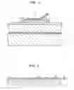
In order to address this problem, in some methods, bonding pads are formed by a material such as Poly-Si that is not etched by a hydrofluoric acid solution, without forming Al bonding pads. However, in this case, Poly-Si is resistant to plastic deformation unlike Al that is susceptible to plastic deformation as described in patent document 1. Thus as shown in FIG. 5, when a Poly-Si film bonding pad 1 has a considerably uneven surface, gaps 3 are formed on a junction when an Al wire 2 is bonded, so that a sufficient bonding area cannot be obtained and the bonding performance may deteriorate. In FIG. 5, reference numeral 1 denotes the Poly-Si film bonding pad, reference numeral 2 denotes the Al wire, and reference numeral 3 denotes the gaps.
DISCLOSURE OF THE INVENTION
The present invention is devised to solve the problem. An object of the present invention is to provide a junction structure and a method of manufacturing the same whereby a Poly-Si film bonding pad and an Al wire can be stably wire bonded even when wedge bonding is performed using the Al wire in the junction structure having the Poly-Si film bonding pad.
In order to attain the object, a junction structure of the present invention includes: a SiO2 film formed on Si; one of a BPSG film and a PSG film formed on the SiO2 film; a SiN film formed on one of the BPSG film and the PSG film; a Poly-Si film formed on the SiN film; and an Al wire bonded on the Poly-Si film.
Further, in the aforementioned configuration, the Poly-Si film has a surface average roughness not larger than the surface roughness of one of the BPSG film and the PSG film.
Moreover, in the aforementioned configuration, the Poly-Si film has a surface roughness not larger than 22 nm.
Further, in the aforementioned configuration, the Poly-Si film has a thickness not smaller than 200 nm.
A method of manufacturing the junction structure of the present invention includes the steps of: forming a SiO2 film on Si; forming one of a BPSG film and a PSG film on the SiO2 film; forming a SiN film on one of the BPSG film and the PSG film; forming a Poly-Si film on the SiN film; and bonding an Al wire on the Poly-Si film.
The junction structure and the method of manufacturing the same according to the present invention do not require a process of forming Al or Au on the Poly-Si film acting as a bonding pad, so that the manufacturing period can be shorter than the manufacturing period of the prior art and a mask for the process can be eliminated. Thus it is possible to manufacture the junction structure of the Poly-Si film and the Al wire with an inexpensive manufacturing process. Further, the present invention can reduce the surface average roughness of the Poly-Si film. Thus gaps between bonding surfaces of the Al wire and the Poly-Si film are reduced and the bonding area is increased, thereby improving wire bonding characteristics.
BRIEF DESCRIPTION OF THE DRAWINGS
FIG. 1 is a sectional view showing a junction structure according to an embodiment of the present invention;
FIG. 2 is an enlarged view showing the surface of a Poly-Si film bonding pad of the junction structure;
FIG. 3 is an enlarged view showing a junction between the Poly-Si film bonding pad and an Al wire of the junction structure;
FIG. 4 shows wire pull test results on a Poly-Si film and the Al wire; and
FIG. 5 is a sectional view showing a junction structure of the prior art.
DESCRIPTION OF THE EMBODIMENTS
A junction structure and a method of manufacturing the same according to an embodiment of the present invention will be described below in accordance with the accompanying drawings.
FIGS. 1 and 2 are a sectional view showing the junction structure according to the embodiment of the present invention, and an enlarged view of the surface of a Poly-Si film bonding pad.
As shown in FIG. 1, in the junction structure according to the embodiment of the present invention, a SiO2 film 5 is formed on Si 4, a BPSG film 6 is formed on the SiO2 film 5, a SiN film 7 is formed on the BPSG film 6, a Poly-Si film bonding pad 1 is formed on the SiN film 7, and an Al wire 2 is bonded on the Poly-Si film bonding pad 1. In FIG. 2, reference numeral 8 denotes a pad surface average roughness.
The junction structure is manufactured as follows:
The SiO2 film 5 is formed on the Si 4 in an atmosphere of oxygen at 1000° C. to 1200° C., and the SiO2 film 5 is reacted by atmospheric pressure CVD in an atmosphere containing SiH4, O2, PH3, and B2H6 gas at 350° C. to 450° C., so that the BPSG film 6 is formed on the SiO2 film 5. Next, the BPSG film 6 is heat treated at 850° C. to 950° C. and is reacted by low pressure CVD in an atmosphere containing SiH2Cl2 and NH3 gas at 700° C. to 800° C., so that the SiN film 7 is formed on the BPSG film 6. Further, the SiN film 7 is reacted by low pressure CVD in an atmosphere containing SiH4 gas at 600° C. to 700° C., so that the Poly-Si film bonding pad 1 is formed on the SiN film 7. At this moment, the pad surface average roughness 8 (see FIG. 2) of the Poly-Si film bonding pad 1 is not larger than the surface roughness of the BPSG film 6. By controlling the surface roughness of the BPSG film 6 thus, the pad surface average roughness 8 of the Poly-Si film bonding pad 1 can be reduced.
FIG. 3 is an enlarged view of a junction between the Poly-Si film bonding pad 1 and the Al wire 2 of FIG. 1. When bonding the Al wire 2 to the Poly-Si film bonding pad 1, a state of the surface of the Poly-Si film bonding pad 1 predominantly affects the plastic deformation of the Al wire 2. In other words, when the Poly-Si film bonding pad 1 has a rough surface, deformation of the Al wire 2 increases gaps 3 between bonding surfaces, resulting in an insufficient bonding strength. By reducing the pad surface average roughness 8 of the Poly-Si film bonding pad 1, the gaps 3 between the bonding surfaces are reduced and thus the bonding area of the Poly-Si film bonding pad 1 and the Al wire 2 is increased when the Al wire 2 is bonded to the Poly-Si film bonding pad 1. Thus it is possible to prevent wire bonding characteristics from deteriorating.
FIG. 4 is a graph showing the relationship between the pad surface average roughness 8 of the Poly-Si film bonding pad 1 and a pull strength obtained when a pull test (tensile test) is conducted after the Poly-Si film bonding pad 1 and the Al wire 2 are wire bonded. According to the experimental results of FIG. 4, in a wire pull test conducted on the junction structure of the Poly-Si film bonding pad 1 and the Al wire 2, when the pad surface average roughness 8 of the Poly-Si film bonding pad 1 is larger than 22 nm, a break occurs on the bonding interface of the Poly-Si film bonding pad 1 and the Al wire 2 and the pull strength decreases. When the pad surface average roughness 8 of the Poly-Si film bonding pad 1 is not larger than 22 nm, a break occurs in the Al wire 2 and a stable pull strength is obtained. As is evident from the results of the pull test, it is considered that bonding between the Poly-Si film bonding pad 1 and the Al wire 2 can be stabilized by reducing the pad surface average roughness 8 of the Poly-Si film bonding pad 1.
When the BPSG film 6 is formed by atmospheric pressure CVD, the surface roughness of the BPSG film 6 is controlled by performing heat treatment at 850° C. to 950° C. with concentration B of 1 wt % or more and concentration P of 5.9 wt % or more, so that the pad surface average roughness 8 of the Poly-Si film bonding pad 1 can be 22 nm or lower. Thus it is possible to stabilize wire bonding characteristics between the Poly-Si film bonding pad 1 and the Al wire 2.
By setting the thickness of the Poly-Si film bonding pad 1 at 200 nm or more, it is possible to prevent a stress applied to the Poly-Si film bonding pad 1 during wire bonding from causing a brittle fracture on a Poly-Si film, and thus stabilize wire bonding without causing exfoliation of the Poly-Si film bonding pad 1.
Further, the aforementioned configuration does not require a process of forming Al or Au on the Poly-Si film bonding pad 1, so that the manufacturing period can be shorter than the manufacturing period of the prior art and a mask for the process can be eliminated. Thus it is possible to provide a junction structure which can stably wire bond the Poly-Si film bonding pad 1 and the Al wire 2 with an inexpensive manufacturing process.
The BPSG film 6 may be an interlayer insulating film such as a PSG film.
Claims
What is claimed is:1. A junction structure comprising:
a SiO2 film formed on Si;
one of a BPSG film and a PSG film formed on the SiO2 film;
a SiN film formed on one of the BPSG film and the PSG film;
a Poly-Si film formed on the SiN film; and
an Al wire bonded on the Poly-Si film.
2. The junction structure according to claim 1, wherein the Poly-Si film has a surface average roughness not larger than a surface roughness of one of the BPSG film and the PSG film.
3. The junction structure according to claim 1, wherein the Poly-Si film has a surface roughness not larger than 22 nm.
4. The junction structure according to claim 1, wherein the Poly-Si film has a thickness not smaller than 200 nm.
5. A method of manufacturing a junction structure, comprising the steps of:
forming a SiO2 film on Si;
forming one of a BPSG film and a PSG film on the SiO2 film;
forming a SiN film on one of the BPSG film and the PSG film;
forming a Poly-Si film on the SiN film; and
bonding an Al wire on the Poly-Si film.
Images & Drawings included:


Sources:
- United States Patent and Trademark Office - verify current appl. status at the USPTO↗
Similar patent applications:
- » 20220241903
Junction structure, method for manufacturing junction structure, and solder ball - » 20160126307
SEMICONDUCTOR DEVICE HAVING SUPER JUNCTION STRUCTURE, METHOD FOR MANUFACTURING THE SAME AND METHOD FOR MANUFACTURING SUPER JUNCTION STRUCTURE - » 20120181653
SEMICONDUCTOR PN JUNCTION STRUCTURE AND MANUFACTURING METHOD THEREOF - » 20100167597
Electrode junction structure and manufacturing method thereof - » 20130256390
Junction material, manufacturing method thereof, and manufacturing method of junction structure - » 20200119187
MOSFET, having a semiconductor base substrate with a super junction structure, method of manufacturing the MOSFET, and power conversion circuit having the MOSFET - » 20200357985
Precursor structure of perpendicularly magnetized film, perpendicularly magnetized film structure and method for manufacturing the same, perpendicular magnetization-type magnetic tunnel junction film in which said structure is used and method for manufacturing the same, and perpendicular magnetization-type magnetic tunnel junction element in which said structure or magnetic tunnel junction film is used - » 20220130584
CIRCUIT STRUCTURE, ELECTRICAL JUNCTION BOX, AND METHOD FOR MANUFACTURING CIRCUIT STRUCTURE - » 20120068298
Semiconductor device having super junction structure and method for manufacturing the same - » 20060043478
Semiconductor device having super junction structure and method for manufacturing the same
Recent applications in this class:
- » 20250167164 2025-05-22
SEMICONDUCTOR PACKAGE - » 20250140735 2025-05-01
DIRECT COPPER WIRE BONDING ON NANOTWIN COPPER STRUCTURES - » 20250125301 2025-04-17
SEMICONDUCTOR DEVICE - » 20250118700 2025-04-10
SEMICONDUCTOR DEVICE AND METHOD OF MANUFACTURING THE SAME - » 20250112197 2025-04-03
WIREBOND MULTICHIP PACKAGE - » 20250105201 2025-03-27
SEMICONDUCTOR PACKAGE INCLUDING A BONDING WIRE - » 20250087622 2025-03-13
SEMICONDUCTOR DEVICE - » 20250087621 2025-03-13
INTERPOSER STRUCTURE AND PACKAGE STRUCTURE - » 20250079390 2025-03-06
SEMICONDUCTOR PACKAGE AND METHOD OF MANUFACTURING THE SEMICONDUCTOR PACKAGE - » 20250079389 2025-03-06
SEMICONDUCTOR DEVICE AND METHOD OF MANUFACTURING THE SAME
Recent applications for this Assignee:
- » 20100163630 2010-07-01
Antenna built-in module, card type information device, and methods for manufacturing them - » 20100119915 2010-05-13
Method for operating fuel cell and fuel cell system - » 20100119891 2010-05-13
Method for operating fuel cell and fuel cell system - » 20100115974 2010-05-13
Start-up control method for refrigeration cycle apparatus and refrigeration cycle control apparatus using the same - » 20100031696 2010-02-11
REFRIGERATING COMPRESSOR AND REFRIGERATING DEVICE USING THE SAME - » 20100030836 2010-02-04
Adder, Synthesis Device Thereof, Synthesis Method, Synthesis Program, and Synthesis Program Storage Medium - » 20100017611 2010-01-21
Authentication system - » 20100017610 2010-01-21
Authentication system - » 20090309983 2009-12-17
Motion detector and image capture device, interchangeable lens and camera system including the motion detector - » 20090266584 2009-10-29
Heat dissipating wiring board, method for manufacturing same, and electric device using heat dissipating wiring board