ADHESIVE FILM FOR SEMICONDUCTOR
US20090198013A1
2009-08-06
11/915,280
2005-10-31
Abstract:
An adhesive film for semiconductor is disclosed. The present invention provides an adhesive film for semiconductor used in semiconductor packaging, comprising an adhesive layer, wherein the adhesive layer has surface tension of 19 to 52 erg/cm at 60 ° C. Accordingly, the adhesive film for semiconductor according to the present invention may prevent bubbles from being formed between the adhesive film and a supporting member by controlling surface tension in an optimum condition, and also obtain higher reliability in use of the adhesive film in the semi-conductor packaging by controlling tackiness and adhesive force in an optimum condition.
Inventors:
- TAE HYUN SUNG 28 🇰🇷 Seoul, South Korea
- Hyuk-Soo MOON 7 🇰🇷 Gyeonggi-do, South Korea
- Kyung Tae Wi 4 🇰🇷 Seoul, South Korea
- Joon-Mo Seo 10 🇰🇷 Gyeonggi-do, South Korea
- Byoung-Un Kang 7 🇰🇷 Gyeonggi-do, South Korea
- Dong-Cheon Shin 7 🇰🇷 Seoul, South Korea
- Jai-Hoon Kim 2 🇰🇷 Seoul, South Korea
Interested in similar patents?
Get notified when new applications in this technology area are published.
Classification:
H01L24/83 » CPC main
Arrangements for connecting or disconnecting semiconductor or solid-state bodies; Methods or apparatus related thereto; Methods for connecting semiconductor or other solid state bodies using means for bonding being attached to, or being formed on, the surface to be connected using a layer connector
C09J7/35 » CPC further
Adhesives in the form of films or foils characterised by the adhesive composition Heat-activated
C09J163/00 » CPC further
Adhesives based on epoxy resins; Adhesives based on derivatives of epoxy resins
H01L24/27 » CPC further
Arrangements for connecting or disconnecting semiconductor or solid-state bodies; Methods or apparatus related thereto; Means for bonding being attached to, or being formed on, the surface to be connected, e.g. chip-to-package, die-attach, "first-level" interconnects; Manufacturing methods related thereto; Layer connectors, e.g. plate connectors, solder or adhesive layers; Manufacturing methods related thereto Manufacturing methods
C09J2203/326 » CPC further
Applications of adhesives in processes or use of adhesives in the form of films or foils for bonding electronic components such as wafers, chips or semiconductors
C09J2301/312 » CPC further
Additional features of adhesives in the form of films or foils characterized by the chemical, physicochemical or physical properties of the adhesive or the carrier parameters being the characterizing feature
C09J2463/00 » CPC further
Presence of epoxy resin
H01L2224/8385 » CPC further
Indexing scheme for arrangements for connecting or disconnecting semiconductor or solid-state bodies and methods related thereto as covered by; Methods for connecting semiconductor or other solid state bodies using means for bonding being attached to, or being formed on, the surface to be connected using a layer connector; Bonding techniques using a polymer adhesive, e.g. an adhesive based on silicone, epoxy, polyimide, polyester
H01L2924/01006 » CPC further
Indexing scheme for arrangements or methods for connecting or disconnecting semiconductor or solid-state bodies as covered by; Chemical elements Carbon [C]
H01L2924/01013 » CPC further
Indexing scheme for arrangements or methods for connecting or disconnecting semiconductor or solid-state bodies as covered by; Chemical elements Aluminum [Al]
H01L2924/01015 » CPC further
Indexing scheme for arrangements or methods for connecting or disconnecting semiconductor or solid-state bodies as covered by; Chemical elements Phosphorus [P]
H01L2924/01033 » CPC further
Indexing scheme for arrangements or methods for connecting or disconnecting semiconductor or solid-state bodies as covered by; Chemical elements Arsenic [As]
H01L2924/01082 » CPC further
Indexing scheme for arrangements or methods for connecting or disconnecting semiconductor or solid-state bodies as covered by; Chemical elements Lead [Pb]
H01L2924/07802 » CPC further
Indexing scheme for arrangements or methods for connecting or disconnecting semiconductor or solid-state bodies as covered by; Polymers; Adhesive characteristics other than chemical not being an ohmic electrical conductor
H01L2924/00014 » CPC further
Indexing scheme for arrangements or methods for connecting or disconnecting semiconductor or solid-state bodies as covered by; Technical content checked by a classifier the subject-matter covered by the group, the symbol of which is combined with the symbol of this group, being disclosed without further technical details
H01L2924/3512 » CPC further
Indexing scheme for arrangements or methods for connecting or disconnecting semiconductor or solid-state bodies as covered by; Technical effects; Mechanical effects; Thermal stress Cracking
H01L2924/0665 » CPC further
Indexing scheme for arrangements or methods for connecting or disconnecting semiconductor or solid-state bodies as covered by; Polymers Epoxy resin
H01L2924/181 » CPC further
Indexing scheme for arrangements or methods for connecting or disconnecting semiconductor or solid-state bodies as covered by; Details of package parts other than the semiconductor or other solid state devices to be connected Encapsulation
H01L2924/05442 » CPC further
Indexing scheme for arrangements or methods for connecting or disconnecting semiconductor or solid-state bodies as covered by; Oxides composed of metals from groups of the periodic table 14th Group SiO
H01L2924/00 » CPC further
Indexing scheme for arrangements or methods for connecting or disconnecting semiconductor or solid-state bodies as covered by
C08L63/00 IPC
Compositions of epoxy resins; Compositions of derivatives of epoxy resins
H01L2924/05432 » CPC further
Indexing scheme for arrangements or methods for connecting or disconnecting semiconductor or solid-state bodies as covered by; Oxides composed of metals from groups of the periodic table 13th Group AlO
H01L2924/05032 » CPC further
Indexing scheme for arrangements or methods for connecting or disconnecting semiconductor or solid-state bodies as covered by; Nitrides composed of metals from groups of the periodic table 13th Group AlN
Description
TECHNICAL FIELD
The present invention relates to an adhesive film, and more specifically to an adhesive film for semiconductor used for adhering a die to a chip-mounting frame in a process of semiconductor packaging.
BACKGROUND ART
Generally, a semiconductor packaging process includes a wafer dicing process for cutting a wafer into units of semiconductor chips; a die adhesion process for adhering the cut semiconductor chips onto a chip-mounting frame, for example a lead frame or substrate such as a printed circuit board (PCB) or a tape wiring board, etc.; a wire adhesion process for electrically connecting the chip-mounting frame to the semi-conductor chip; and a packaging process by a epoxy molding compound (EMC) for sealing the semiconductor chip and an adhesive wire.
An adhesive film or an adhesive has been used generally for carrying out bonds between various corresponding elements, for example a semiconductor chip and a substrate, a lead frame and a chip, and a chip and a chip in such a semiconductor packaging process. In the recent years, reduction in weight, thickness, length and size, and high performance of electronic equipment are required in the semiconductor packaging process as a field of electronics/electrics continues to develop. And also a more precisely controllable adhesive continues to be developed in order to facilitate contact between microcircuits, or between a micro-part and a microcircuit.
However, the conventional adhesives is a cause that bubbles are formed in the interface between an adhesive and a supporting member such as a lead frame, substrate or other chip etc., resulting in peeling of package interface due to thermal treatment upon mounting a chip.
Also, a surface-mounting type, which allows the high-density mounting depending on reduction in weight, thickness, length and size of electronic equipment, is mainly used increasingly, but the entire surface-mounting package should be heated because the lead is directly adhered to a printed circuit board in this surface-mounting package. At this time, the package may be cracked by its internal moisture evaporation because it is exposed to high temperature of 200 to 270° C. That is to say, the moisture adsorbed into the adhesive film is vaporized at a mounting temperature, and then cracks are formed between the adhesive film and the supporting member due to pressure by evaporation.
DISCLOSURE OF INVENTION
Technical Problem
Therefore, the present invention is designed to solve the problems of the prior art, and it is an object of the present invention to provide an adhesive composition for an adhesive film in the field of semiconductor-packaging, which may prevent bubbles from being formed between an adhesive film and a supporting member by controlling surface tension in an optimum condition, and obtain reliability of semiconductor packaging by controlling tackiness and adhesive force in an optimum condition, and an adhesive film using same.
Technical Solution
In order to accomplish the above object, the present invention provides an adhesive film to be used in a semiconductor packaging, comprising an adhesive layer; wherein the adhesive layer has surface tension of 19 to 52 erg/cm2 at 60° C.
Preferably, the adhesive layer may have tackiness of 50 to 400 gf/Ø5.0 mm at 60 ° C.
More preferably, the adhesive layer may have adhesive force of at least 5 gf/cm2.
Meanwhile, the adhesive layer preferably includes at least one material selected from the group consisting of an epoxy-based resin, an organic filler, an inorganic filler and a curing agent, and further may include at least one modifier selected from the group consisting of a amino-based compound, a silane-based compound, an acrylic compound, metal organic salt, silicon oxide and titanium oxide.
BRIEF DESCRIPTION OF THE DRAWINGS
These and other features, aspects, and advantages of preferred embodiments of the present invention will be more fully described in the following detailed description, taken accompanying drawings. In the drawings:
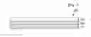
FIG. 1 is a cross-sectional view showing an adhesive film according to a preferred embodiment of the present invention.
BEST MODE FOR CARRYING OUT THE INVENTION
Hereinafter, preferred embodiments of the present invention will be described in detail referring to the accompanying drawing. Prior to the description, it should be understood that the terms used in the specification and appended claims should not be construed as limited to general and dictionary meanings, but interpreted based on the meanings and concepts corresponding to technical aspects of the present invention on the basis of the principle that the inventor is allowed to define terms appropriately for the best explanation. Therefore, the description proposed herein is just a preferable example for the purpose of illustrations only, not intended to limit the scope of the invention, so it should be understood that other equivalents and modifications could be made thereto without departing from the spirit and scope of the invention.
FIG. 1 is a cross-sectional view showing an adhesive film according to a preferred embodiment of the present invention.
Referring to FIG. 1, an adhesive film 100 according to this embodiment includes a base film 110; an adhesive layer 120 adhered to one surface of the base film 110; and a protective film 111 adhered to the other surface of the adhesive layer 120. The protective film 111 functions to protect the adhesive layer 120.
The base film 110, which maintains a basic form of the adhesive film, may preferably include polyethylene terephthalate (PET) or polyethylene- polyethylene-2,6-naphthalenedicarboxylate (PEN).
The protective film 111, which protects the adhesive layer from foreign substances, may preferably include polyethylene or polyethylene terephthalate (PET).
The adhesive layer 120 is adhered between a die and a supporting member, for example a lead frame, a substrate or other dies after the base film 110 and the protective film 111 are removed.
An adhesive film 100 is laminated into the supporting member at a ranges of 60 to 80° C., or pressed into the supporting member at a ranges of 110 to 130° C. In this case, bubbles may be generated between the adhesive film and the supporting member if surface tension of an adhesive layer 120 in the adhesive film 100 is widely different to that of the supporting member in the lamination process. Accordingly, surface tension of the adhesive layer 120 is set to surface tension of the supporting member, for example a range of 19 to 52 erg/cm2 to give a smooth surface and good wetness of the supporting member.
Preferably, tackiness of the adhesive layer 120 is set to 50 to 400 gf/Ø05.0 mm. It is because that if the adhesive layer 120 has tackiness of less than 50 gf/Ø5.0 mm, the supporting member and the adhesive film 100 may not be sufficiently adhered each other, causing formation of bubbles in their interface, and that if the adhesive layer 120 has tackiness of at least 400 gf/Ø5.0 mm, it may have a disadvantage that a double-faced adhesive film is strongly adhered to and not detached from the equipment.
More preferably, the adhesive layer 120 has adhesive force of at lease 5 gf/cm2. If it has adhesive force of less than 5 gf/cm2, it is difficult to obtain enough adhesive force to prevent bubbles being formed in surfaces of the adhesive layer 120 during the adhesion process.
Meanwhile, a composition constituting the adhesive layer 120 may includes at least one material selected from the group consisting of an epoxy-based resin, an organic filler, a curing agent and an inorganic filler. The epoxy-based resin may be preferably used by mixing a solid-phase epoxy resin and a liquid-phase epoxy resin. And bisphenol A, bisphenol F, a phenoxy resin or a cresol novolac resin may be also used. Such epoxy resin may give a high adhesive strength, and has very low reaction shrinkage and no generation of volatile materials. Also it has excellent properties such as a mechanical property, an electric insulating property, water resistance, and thermal resistance.
The organic filler may include polyimide, polyamideimide, polyesterimide, nylon, or silicon resin etc. The inorganic filler may include silica, aluminum nitride, or alumina etc. The curing agent may include amines, anhydrides, or amides etc., and further include a latent curing agent and a curing agent with high melting point. Preferably, the adhesive layer may further include a metal filler to give an electro-conductive property.
In addition, a composition constituting the adhesive layer 120 preferably includes at least one modifier selected from the group consisting of a amino-based compound, a silane-based compound, an acrylic compound, metal organic salt, silicon oxide and titanium oxide. Such modifier may be added to adjust surface tension, tackiness, and adhesive force of the adhesive layer 120 in an optimum condition.
However, the present invention is not limited to the materials, but various changes and modifications within the spirit and scope of the invention may be adapted by those skilled in the art from this detailed description.
Hereinafter, the present invention will be described in detail with specific example. However, it should be understood that the detailed description and specific examples according to preferred embodiments of the invention, are given by way of illustration only, since various changes and modifications within the spirit and scope of the invention will become apparent to those skilled in the art from this detailed description.
A solid-phase epoxy resin, a liquid-phase epoxy resin, an organic filler, an epoxy curing agent, a UV-curing agent and a UV-curing formulation were mixed in a constant ratio in Examples 1 to 3, and Comparative examples 1 and 2, and various modifiers were further added and mixed in Examples 1 to 3. Subsequently, each mixture was coated into a 50 □-thick polyester film in thickness about 25 □. Ratios of such compositions of Examples and Comparative examples are listed in Table 1 as follows.
| TABLE 1 | ||
| Example | Comparative example |
| 1 | 2 | 3 | 1 | 2 | |
| Solid-phase epoxy | 35 | 35 | 40 | 30 | 40 |
| Liquid-phase epoxy | 30 | 30 | 25 | 35 | 25 |
| Organic filler | 29 | 29 | 29 | 29 | 29 |
| Modifier | 1 phr | 5 phr | 10 phr | 0 phr | 15 phr |
| Epoxy curing agent | 4 phr | 4 phr | 4 phr | 4 phr | 4 phr |
| UV-curing agent | 6 phr | 6 phr | 6 phr | 6 phr | 6 phr |
| UV-curing formulation | 6 | 6 | 6 | 6 | 6 |
In compositional ratios of Examples and Comparative examples listed in the Table 1, the modifier, the epoxy curing agent, and the UV-curing agent were added in “part by weight”, based on 100% by weight of a solid-phase epoxy, a liquid-phase epoxy, an organic filler and a UV-curing formulation.
Surface tension, tackiness, and 180° peel strength of Examples 1 to 3, Comparative examples 1 and 2 having the compositions listed in the Table 1 were measured and the results are listed in Table 2.
| TABLE 2 | ||
| Example | Comparative example |
| 1 | 2 | 3 | 1 | 2 | |
| Surface tension (60° C.)(erg/□) | 52 | 39 | 19 | 58 | 13 |
| Tackiness (60° C.) (gf) | 102 | 89 | 82 | 330 | 55 |
| 180° peel strength | 60° C. | 150 | 110 | 75 | 130 | 10 |
| (gf/cm)(adhesive force) | After | 1,100 | 1,120 | 580 | 450 | 320 |
| cured |
| MRT test(JEDEC Level | Passed | Passed | Passed | No passed | No passed |
| 1Pb-free) | |||||
Referring to Table 2, the compositions of Examples 1 to 3 having surface tension of 19 to 52 erg/cm2 showed an excellent properties when MRT test was carried out according to a procedure specified in JEDEC. That is to say, a good wetness of the supporting member also possibly prevents the bubbles being generated between the adhesive film and a supporting member, which eventually prevents cracking of the semiconductor package. Also as shown in Table 2, tackiness and adhesive force may be maintained at a suitable level to prevent the adhesive layer from remaining in the press machine due to excessive tackiness in a pressing process of the adhesive film.
The present invention has been described in detail. However, it should be understood that the detailed description and specific examples according to preferred embodiments of the invention, are given by way of illustration only, since various changes and modifications within the spirit and scope of the invention will become apparent to those skilled in the art from this detailed description.
INDUSTRIAL APPLICABILITY
As been described above, the adhesive film for semiconductor according to the present invention may be useful to prevent bubbles from being formed between the adhesive film and a supporting member by controlling surface tension in an optimum condition and also obtain higher reliability in use of the adhesive film in semi-conductor packaging by controlling tackiness and adhesive force in an optimum condition.
Claims
1. An adhesive film for semiconductor used in a semiconductor packaging, comprising an adhesive layer;
wherein the adhesive layer has surface tension of 19 to 52 erg/cm2 at 60° C.
2. The adhesive film for semiconductor according to the claim 1, wherein the adhesive layer has tackiness of 50 to 400 gf/Ø5.0 mm at 60° C.
3. The adhesive film for semiconductor according to the claim 1, wherein the adhesive layer has adhesive force of at least 5 gf/cm2.
4. The adhesive film for semiconductor according to claim 1,
wherein the adhesive layer includes at least one material selected from the group consisting of an epoxy-based resin, an organic filler, an inorganic filler and a curing agent.
5. The adhesive film for semiconductor according to the claim 4, wherein the adhesive layer further includes at least one modifier selected from the group consisting of a amino-based compound, a silane-based compound, an acrylic compound, metal organic salt, silicon oxide and titanium oxide.
6. The adhesive film for semiconductor according to claim 2, wherein the adhesive layer includes at least one material selected from the group consisting of an epoxy-based resin, an organic filler, an inorganic filler and a curing agent.
7. The adhesive film for semiconductor according to claim 3, wherein the adhesive layer includes at least one material selected from the group consisting of an epoxy-based resin, an organic filler, an inorganic filler and a curing agent.
8. The adhesive film for semiconductor according to the claim 6, wherein the adhesive layer further includes at least one modifier selected from the group consisting of a amino-based compound, a silane-based compound, an acrylic compound, metal organic salt, silicon oxide and titanium oxide.
9. The adhesive film for semiconductor according to the claim 7, wherein the adhesive layer further includes at least one modifier selected from the group consisting of a amino-based compound, a silane-based compound, an acrylic compound, metal organic salt, silicon oxide and titanium oxide.
Images & Drawings included:

Sources:
- United States Patent and Trademark Office - verify current appl. status at the USPTO↗
Similar patent applications:
- » 20110152394
Adhesive composition for stealth dicing of semiconductor, adhesive film, and semiconductor device including the adhesive film - » 20060043607
Adhesive film for semiconductor, metal sheet with such adhesive film, wiring substrate with adhesive film, semiconductor device, and method for manufacturing semiconductor device - » 20110006441
RESIN VARNISH USED FOR ADHESIVE FILM FOR SEMICONDUCTOR ELEMENT, ADHESIVE FILM FOR SEMICONDUCTOR ELEMENT, AND SEMICONDUCTOR DEVICE - » 20220089916
Adhesive resin composition for semiconductor, adhesive film for semiconductor device using the same and dicing die bonding film using the same - » 20190043748
Adhesive resin composition for semiconductor, adhesive film for semiconductor, and dicing die bonding film - » 20210009867
Resin composition for bonding semiconductors, adhesive film for semiconductor using the same, dicing die bonding film, and method for dicing semiconductor wafer - » 20170198182
Adhesive composition for semiconductor, adhesive film for semiconductor, and dicing die bonding film - » 20090053498
ADHESIVE FILM FOR SEMICONDUCTOR USE, METAL SHEET LAMINATED WITH ADHESIVE FILM, WIRING CIRCUIT LAMINATED WITH ADHESIVE FILM, AND SEMICONDUCTOR DEVICE USING SAME, AND METHOD FOR PRODUCING SEMICONDUCTOR DEVICE - » 20090091012
Thermoplastic resin composition for semiconductor, adhesion film, lead frame, and semiconductor device using the same, and method of producing semiconductor device - » 20140186607
ADHESIVE COMPOSITION FOR A SEMICONDUCTOR, ADHESIVE FILM PREPARED FROM THE COMPOSITION, AND SEMICONDUCTOR DEVICE CONNECTED BY THE FILM
Recent applications in this class:
- » 20250167170 2025-05-22
LASER TRANSFER OF MICROELECTRONIC DEVICE AND ASSOCIATED CONDUCTIVE PAD - » 20250140738 2025-05-01
SEMICONDUCTOR MANUFACTURING APPARATUS, METHOD OF MANUFACTURING SEMICONDUCTOR APPARATUS, AND SEMICONDUCTOR APPARATUS - » 20250132288 2025-04-24
PROCESS FOR FLIP CHIP PACKAGING - » 20250125304 2025-04-17
METHOD OF MANUFACTURING A CHIP STRUCTURE AND CHIP STRUCTURE - » 20250087628 2025-03-13
METHOD OF SURFACE MODIFICATION FOR WAFER BONDING - » 20250079395 2025-03-06
METHOD OF MANUFACTURING SEMICONDUCTOR PACKAGE - » 20250070080 2025-02-27
METHOD OF BONDING CHIPS AND A SYSTEM FOR PERFORMING THE METHOD - » 20250062276 2025-02-20
METHOD FOR DIPPING ADHESIVE MATERIAL - » 20250046751 2025-02-06
CONTROLLING ADHESIVE REFLOW FOR TRANSFER PRINTING - » 20250022842 2025-01-16
SEMICONDUCTOR PACKAGE