METHOD OF MANUFACTURING SEMICONDUCTOR DEVICE
US20100068853A1
2010-03-18
12/561,003
2009-09-16
Abstract:
In a method of manufacturing a semiconductor device, a substrate having first electrodes on a main surface thereof and a semiconductor chip having second electrodes on a first main surface thereof are arranged such that the main surface of the substrate and the first main surface of the semiconductor chip oppose to each other, and the first electrodes and the second electrodes are connected so as to electrically connect the substrate and the semiconductor chip. The semiconductor chip is made thin by grinding a second main surface opposing to the first main surface of the semiconductor chip which is connected with the substrate. Side surfaces and the second main surface of the semiconductor chip made thin are sealed with resin.
Assignee:
- NEC Electronics Corporation 1,669 🇯🇵 Kawasaki, Japan
Interested in similar patents?
Get notified when new applications in this technology area are published.
Classification:
H01L21/561 » CPC further
Processes or apparatus adapted for the manufacture or treatment of semiconductor or solid state devices or of parts thereof; Manufacture or treatment of semiconductor devices or of parts thereof the devices having at least one potential-jump barrier or surface barrier, e.g. PN junction, depletion layer or carrier concentration layer; Assembly of semiconductor devices using processes or apparatus not provided for in a single one of the subgroups - , e.g. sealing of a cap to a base of a container; Encapsulations, e.g. encapsulation layers, coatings Batch processing
H01L23/3121 » CPC further
Details of semiconductor or other solid state devices; Encapsulations, e.g. encapsulating layers, coatings, e.g. for protection characterised by the arrangement or shape the device being completely enclosed a substrate forming part of the encapsulation
H01L24/97 » CPC further
Arrangements for connecting or disconnecting semiconductor or solid-state bodies; Methods or apparatus related thereto; Batch processes at chip-level, i.e. with connecting carried out on a plurality of singulated devices, i.e. on diced chips the devices being connected to a common substrate, e.g. interposer, said common substrate being separable into individual assemblies after connecting
H01L21/563 » CPC further
Processes or apparatus adapted for the manufacture or treatment of semiconductor or solid state devices or of parts thereof; Manufacture or treatment of semiconductor devices or of parts thereof the devices having at least one potential-jump barrier or surface barrier, e.g. PN junction, depletion layer or carrier concentration layer; Assembly of semiconductor devices using processes or apparatus not provided for in a single one of the subgroups - , e.g. sealing of a cap to a base of a container; Encapsulations, e.g. encapsulation layers, coatings Encapsulation of active face of flip-chip device, e.g. underfilling or underencapsulation of flip-chip, encapsulation preform on chip or mounting substrate
H01L24/16 » CPC further
Arrangements for connecting or disconnecting semiconductor or solid-state bodies; Methods or apparatus related thereto; Means for bonding being attached to, or being formed on, the surface to be connected, e.g. chip-to-package, die-attach, "first-level" interconnects; Manufacturing methods related thereto; Bump connectors ; Manufacturing methods related thereto; Structure, shape, material or disposition of the bump connectors after the connecting process of an individual bump connector
H01L2224/0554 » CPC further
Indexing scheme for arrangements for connecting or disconnecting semiconductor or solid-state bodies and methods related thereto as covered by; Means for bonding being attached to, or being formed on, the surface to be connected, e.g. chip-to-package, die-attach, "first-level" interconnects; Manufacturing methods related thereto; Bonding areas; Manufacturing methods related thereto; Structure, shape, material or disposition of the bonding areas prior to the connecting process of an individual bonding area External layer
H01L2224/05573 » CPC further
Indexing scheme for arrangements for connecting or disconnecting semiconductor or solid-state bodies and methods related thereto as covered by; Means for bonding being attached to, or being formed on, the surface to be connected, e.g. chip-to-package, die-attach, "first-level" interconnects; Manufacturing methods related thereto; Bonding areas; Manufacturing methods related thereto; Structure, shape, material or disposition of the bonding areas prior to the connecting process of an individual bonding area; External layer Single external layer
H01L2224/16 » CPC further
Indexing scheme for arrangements for connecting or disconnecting semiconductor or solid-state bodies and methods related thereto as covered by; Means for bonding being attached to, or being formed on, the surface to be connected, e.g. chip-to-package, die-attach, "first-level" interconnects; Manufacturing methods related thereto; Bump connectors; Manufacturing methods related thereto; Structure, shape, material or disposition of the bump connectors after the connecting process of an individual bump connector
H01L2924/01005 » CPC further
Indexing scheme for arrangements or methods for connecting or disconnecting semiconductor or solid-state bodies as covered by; Chemical elements Boron [B]
H01L2924/01006 » CPC further
Indexing scheme for arrangements or methods for connecting or disconnecting semiconductor or solid-state bodies as covered by; Chemical elements Carbon [C]
H01L2924/01033 » CPC further
Indexing scheme for arrangements or methods for connecting or disconnecting semiconductor or solid-state bodies as covered by; Chemical elements Arsenic [As]
H01L2924/01079 » CPC further
Indexing scheme for arrangements or methods for connecting or disconnecting semiconductor or solid-state bodies as covered by; Chemical elements Gold [Au]
H01L2224/97 » CPC further
Indexing scheme for arrangements for connecting or disconnecting semiconductor or solid-state bodies and methods related thereto as covered by; Batch processes at chip-level, i.e. with connecting carried out on a plurality of singulated devices, i.e. on diced chips the devices being connected to a common substrate, e.g. interposer, said common substrate being separable into individual assemblies after connecting
H01L2224/81 » CPC further
Indexing scheme for arrangements for connecting or disconnecting semiconductor or solid-state bodies and methods related thereto as covered by; Methods for connecting semiconductor or other solid state bodies using means for bonding being attached to, or being formed on, the surface to be connected using a bump connector
H01L2224/05599 » CPC further
Indexing scheme for arrangements for connecting or disconnecting semiconductor or solid-state bodies and methods related thereto as covered by; Means for bonding being attached to, or being formed on, the surface to be connected, e.g. chip-to-package, die-attach, "first-level" interconnects; Manufacturing methods related thereto; Bonding areas; Manufacturing methods related thereto; Structure, shape, material or disposition of the bonding areas prior to the connecting process of an individual bonding area; External layer Material
H01L2224/0555 » CPC further
Indexing scheme for arrangements for connecting or disconnecting semiconductor or solid-state bodies and methods related thereto as covered by; Means for bonding being attached to, or being formed on, the surface to be connected, e.g. chip-to-package, die-attach, "first-level" interconnects; Manufacturing methods related thereto; Bonding areas; Manufacturing methods related thereto; Structure, shape, material or disposition of the bonding areas prior to the connecting process of an individual bonding area; External layer Shape
H01L2924/00014 » CPC further
Indexing scheme for arrangements or methods for connecting or disconnecting semiconductor or solid-state bodies as covered by; Technical content checked by a classifier the subject-matter covered by the group, the symbol of which is combined with the symbol of this group, being disclosed without further technical details
H01L2224/0556 » CPC further
Indexing scheme for arrangements for connecting or disconnecting semiconductor or solid-state bodies and methods related thereto as covered by; Means for bonding being attached to, or being formed on, the surface to be connected, e.g. chip-to-package, die-attach, "first-level" interconnects; Manufacturing methods related thereto; Bonding areas; Manufacturing methods related thereto; Structure, shape, material or disposition of the bonding areas prior to the connecting process of an individual bonding area; External layer Disposition
H01L21/78 » CPC main
Processes or apparatus adapted for the manufacture or treatment of semiconductor or solid state devices or of parts thereof; Manufacture or treatment of devices consisting of a plurality of solid state components formed in or on a common substrate or of parts thereof; Manufacture of integrated circuit devices or of parts thereof; Manufacture or treatment of devices consisting of a plurality of solid state components or integrated circuits formed in, or on, a common substrate with subsequent division of the substrate into plural individual devices
H01L21/50 IPC
Processes or apparatus adapted for the manufacture or treatment of semiconductor or solid state devices or of parts thereof; Manufacture or treatment of semiconductor devices or of parts thereof the devices having at least one potential-jump barrier or surface barrier, e.g. PN junction, depletion layer or carrier concentration layer Assembly of semiconductor devices using processes or apparatus not provided for in a single one of the subgroups - , e.g. sealing of a cap to a base of a container
Description
INCORPORATION BY REFERENCE
This patent application claims a priority on convention based on Japanese Patent Application No. 2008-238103. The disclosure thereof is incorporated herein by reference.
BACKGROUND OF THE INVENTION
1. Field of the Invention
The present invention relates to a method of manufacturing a resin sealed type of semiconductor device.
2. Description of Related Art
In a Ball Grid Array (BGA) package to realize a multi-pin type of semiconductor device and an excellent electronic characteristic thereof, the thickness of a package is determined depending on the thicknesses of a semiconductor chip allocated in the package. The package has a certain thickness since a defect such as a crack may be generated in a dicing step in the assembly of a semiconductor device unless the semiconductor chip has a certain degree of thickness. However, in order to mount a high-performance chip in a limited space, a further thinning of a package is a necessary technique.
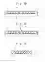
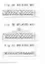
A method of manufacturing semiconductor device by using a package thinning technique is described in Japanese Patent Application Publication No. 2004-158739. The method is shown in FIGS. 3A to 3F. FIG. 3A shows a bonding step of semiconductor chips. As shown in FIG. 3A, a substrate 1 such as a polyimide substrate having electrodes made of Au on its surface and semiconductor chips 4 having bumps 3 made of Au on its surface are prepared. By arranging the semiconductor chips 4 in such a manner that their surfaces face the surface of the substrate 1, the electrodes of the substrate 1 are connected to the bumps 3 so as to bond the semiconductor chips 4 to the substrate 1. After that, the surface of the substrate 1 facing the bumps 3 thereon, side surfaces of the semiconductor chips 4, and rear surfaces of the semiconductor chips 4 are molded with an epoxy resin 5.
Next, as shown in FIG. 3B, by grinding the resin 5 on the rear surfaces of the semiconductor chips 4 by a grinder 6, the rear surfaces of the semiconductor chips 4 are exposed. Then, as shown in FIG. 3C, the semiconductor chips 4 are thinned to about 50 μm, for example. According to this step, the rear surfaces of the semiconductor chips 4 and the surface of the resin 5 are formed on a same plane.
Then, as shown in FIG. 3D, as a conductive film, a metal layer 7 is formed on the rear surfaces of the semiconductor chips 4 and the surface of the resin 5 of the opposite side portions of each of the semiconductor chips 4. This metal layer 7 is formed to have a laminate structure having a TiN layer of 100 ·m or less and an Au layer of about 50 ·m, in order to maintain an adhesion. Further, the metal layer 7 may be made of other metal or a metal compound, and a resin layer may be formed in place of the metal layer 7.
At last, as shown in FIG. 3E, by grinding the space between the semiconductor chips by using a dicing saw 8, semiconductor devices of a resin sealed type are individually diced, as shown in FIG. 3F. In the resin sealed type of semiconductor device diced by this dicing step, any surfaces of the semiconductor chip 4 are not exposed.
However, according to such a method, as shown in FIG. 3D, the metal layer 7 should be formed after grinding the resin 5 and the semiconductor chips 4. In this case, because of a stress caused by change in a temperature of the resin sealed type of semiconductor device, a difference in a coefficient of thermal expansion between the metal layer 7 and the resin 5 may involve a problem of adhesion of the semiconductor chips 4 and their peripheral parts.
SUMMARY OF THE INVENTION
In an aspect of the present invention, a method of manufacturing a semiconductor device is achieved by arranging a substrate having first electrodes on a main surface thereof and a semiconductor chip having second electrodes on a first main surface thereof such that the main surface of the substrate and the first main surface of the semiconductor chip oppose to each other and connecting the first electrodes and the second electrodes so as to electrically connect the substrate and the semiconductor chip; by making the semiconductor chip thin by grinding a second main surface opposing to the first main surface of the semiconductor chip which is connected with the substrate; and by sealing side surfaces and the second main surface of the semiconductor chip made thin, with resin.
In another aspect of the present invention, a method of manufacturing a semiconductor device is achieved by mounting a semiconductor chip having a predetermined thickness above a substrate such that the semiconductor chip is electrically connected with the substrate; by grinding the semiconductor chip to a thickness thinner than the predetermined thickness; and by sealing the substrate and the semiconductor chip with resin to cover the main surface of the substrate and the semiconductor chip.
BRIEF DESCRIPTION OF THE DRAWINGS
The above and other objects, advantages and features of the present invention will be more apparent from the following description of certain embodiments taken in conjunction with the accompanying drawings, in which:
FIG. 1 is a diagram showing a structure of a resin sealed type of semiconductor device according to an embodiment of the present invention;
FIGS. 2A to 2F are sectional views showing a manufacturing method of the resin sealed type of semiconductor device according to the embodiment of the present invention; and
FIGS. 3A to 3F are sectional views showing a conventional manufacturing method of the resin sealed type of semiconductor device.
DESCRIPTION OF THE PREFERRED EMBODIMENTS
Hereinafter, a method of manufacturing a resin sealed type of semiconductor device according to the present invention will be described with reference to the attached drawings.
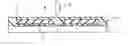
FIG. 1 is a sectional view showing a structure of a resin sealed type of semiconductor device 10 according to an embodiment of the present invention. As shown in FIG. 1, the resin sealed type of semiconductor device 10 according to the present embodiment is provided with a substrate 1, an underfill 2, bumps 3, a semiconductor chip 4, and a resin 5.
First electrodes 12 made of Au are formed on a surface (a main surface) of the substrate 1 such as a polyimide substrate. In addition, second electrodes 11 are formed on the surface (a first main surface) of the semiconductor chip 4, and the bumps 3 made of Au are formed on the second electrodes 12. The first main surface of the semiconductor chip 4 and the main surface of the substrate 1 are arranged so as to face to each other. In addition, the substrate 1 and the semiconductor chip 4 are bonded with each other via the underfill 2 such as a resin, and the first electrodes 12 of the substrate 1 and the second electrodes 11 are connected via the bumps 3. In other words, the semiconductor chip 4 is mounted on the substrate 1 facedown.
Epoxy resin 5 is formed on the main surface (the surface on the part of the bumps 3) of the substrate 1 so as to cover the semiconductor chip 4. In other words, the main surface of the substrate 1, and the side surfaces and the rear surface (the second main surface) of the semiconductor chip 4 are molded with the resin 5. Further, the semiconductor chip 4 is thinned to about 50 ·m, for example.
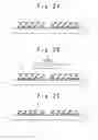
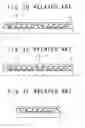
Here, referring to FIGS. 2A to 2F, a method of manufacturing the resin sealed type of semiconductor device 10 according to the embodiment of the present invention will be described. FIGS. 2A to 2F are sectional views in the manufacturing method of the resin sealed semiconductor device 10 according to the present embodiment. In this case, an example such that two semiconductor chips 4 are bonded with each other on the substrate 1 is illustrated.
FIG. 2A shows a bonding step of the semiconductor chips. As shown in FIG. 2A, at first, the substrate 1 having the first electrodes 12 on the surface thereof and the semiconductor chips 4 having the bumps 3 on the second electrodes 12 are prepared. Each of the semiconductor chips 4 has a predetermined thickness. Then, by arranging the semiconductor chips 4 in such a manner that their surfaces face the surface of the substrate 1, the first electrodes 12 of the substrate 1 are connected to the second electrodes 11 via the bumps 3. Thereby, the semiconductor chips having predetermined thicknesses are mounted on the substrate 1. Then, the semiconductor chips 4 are bonded to the substrate 1 by forming the underfill 2 in the gap between the substrate 1 and each of the semiconductor chips 4.
Next, as shown in FIG. 2B, by grinding the rear surfaces of the semiconductor chips 4 by using a grinder 6, the semiconductor chips 4 are thinned more than the above-described predetermined thicknesses as shown in FIG. 2C. For example, the semiconductor chips 4 are thinned to about 50 ·m, for example.
Subsequently, as shown in FIG. 2D, the resin 5 is formed so as to cover a plurality of the semiconductor chips 4. Depending on this step, the side surfaces and the rear surfaces of the semiconductor chips 4 are covered with the resin 5, and any surfaces of the semiconductor chip 4 are not exposed. In other words, the surfaces of the semiconductor chips 4 except for the surfaces connected with the substrate 1 are covered with the resin 5. In addition, a region not covered with the semiconductor chips 4 on the surface of the substrate 1 are also covered with the resin 5.
Finally, by grinding the gap between the semiconductor chips 4 by using a dicing saw 8 as shown in FIG. 2E, the resin sealed type of semiconductor devices 10 are individually diced as shown in FIG. 2F. Even after this dicing step, in each of the resin sealed type of semiconductor devices 10, any surfaces of the semiconductor chips 4 are covered with the resin 5 and they are not exposed.
In this manner, the resin sealed type of semiconductor device 10 according to the present invention is constructed in such a manner that the semiconductor chips 4 are bonded to the substrate 1, and after dicing the semiconductor chips 4, any surfaces of the semiconductor chips 4 are covered with the resin 5 so that any surfaces of the semiconductor chips 4 are not exposed. Therefore, there is no need to form another film after dicing the semiconductor chips 4, and the semiconductor chips 4 can be collectively covered with the resin 5. This provides an effect that no boundary face exists between the resin 5 and another layer and the resin itself has an excellent adhesion with respect to the semiconductor chips, unlike a conventional case.
As described above, according to the present invention, as compared to a conventional manufacturing method of the resin sealed type of semiconductor device in which a metal film is formed after dicing of the semiconductor chips, the adhesion between the semiconductor chips and the resin can be improved. In addition, according to the present invention, the conventional step of forming a metal layer can be omitted, and this makes it possible to simplify the manufacturing method of the resin sealed semiconductor device.
Although the present invention has been described above in connection with several embodiments thereof, it would be apparent to those skilled in the art that those embodiments are provided solely for illustrating the present invention, and should not be relied upon to construe the appended claims in a limiting sense.
Claims
What is claimed is:1. A method of manufacturing a semiconductor device comprising:
arranging a substrate having first electrodes on a main surface thereof and a semiconductor chip having second electrodes on a first main surface thereof such that the main surface of said substrate and the first main surface of said semiconductor chip oppose to each other and connecting said first electrodes and said second electrodes so as to electrically connect said substrate and said semiconductor chip;
making said semiconductor chip thin by grinding a second main surface opposing to the first main surface of said semiconductor chip which is connected with said substrate; and
sealing side surfaces and said second main surface of said semiconductor chip made thin, with resin.
2. The method according to claim 1, wherein a plurality of said semiconductor chips are connected to said substrate, and
said method further comprises:
individually dicing said plurality of semiconductor chips after said sealing of said plurality of semiconductor chips with said resin.
3. The method according to claim 1, further comprising:
forming underfill in a space between the main surface of said substrate and the first main surface of said semiconductor chip.
4. The method according to claim 2, further comprising:
forming underfill in a space between the main surface of said substrate and the first main surface of each of said plurality of semiconductor chips.
5. A method of manufacturing a semiconductor device comprising:
mounting a semiconductor chip having a predetermined thickness above a substrate such that said semiconductor chip is electrically connected with said substrate;
grinding said semiconductor chip to a thickness thinner than the predetermined thickness; and
sealing said substrate and said semiconductor chip with resin to cover the main surface of said substrate and said semiconductor chip.
Images & Drawings included:
Sources:
- United States Patent and Trademark Office - verify current appl. status at the USPTO↗
Similar patent applications:
- » 20100193792
LAMINATED FILM MANUFACTURING METHOD, SEMICONDUCTOR DEVICE MANUFACTURING METHOD, SEMICONDUCTOR DEVICE AND DISPLAY DEVICE - » 20230187203
Semiconductor device manufacturing method, semiconductor memory device manufacturing method, semiconductor memory device, and substrate treatment apparatus - » 20090233430
SEMICONDUCTOR DEVICE MANUFACTURING METHOD, SEMICONDUCTOR DEVICE MANUFACTURING APPARATUS, AND SEMICONDUCTOR DEVICE MANUFACTURING SYSTEM - » 20090166516
Photoelectric conversion device manufacturing method, semiconductor device manufacturing method, photoelectric conversion device, and image sensing system - » 20070177126
Wafer flatness evaluation method, wafer flatness evaluation apparatus carrying out the evaluation method, wafer manufacturing method using the evaluation method, wafer quality assurance method using the evaluation method, semiconductor device manufacturing method using the evaluation method and semiconductor device manufacturing method using a wafer evaluated by the evaluation method - » 20090032950
Film forming method, semiconductor device manufacturing method, semiconductor device, program and recording medium - » 20090214964
Semiconductor device manufacturing method, semiconductor device manufacturing equipment, and computer readable medium - » 20070090093
Semiconductor device manufacturing method, semiconductor device manufacturing apparatus, control program and computer storage medium - » 20070177127
Wafer flatness evaluation method, wafer flatness evaluation apparatus carrying out the evaluation method, wafer manufacturing method using the evaluation method, wafer quality assurance method using the evaluation method, semiconductor device manufacturing method using the evaluation method and semiconductor device manufacturing method using a wafer evaluated by the evaluation method - » 20100015799
Semiconductor device manufacturing method, semiconductor device manufacturing apparatus, computer program and storage medium
Recent applications in this class:
- » 20250167049 2025-05-22
WAFER PROCESSING METHOD - » 20250157858 2025-05-15
LASER DICING FOR SINGULATION - » 20250157857 2025-05-15
COMPONENT AND METHOD OF MANUFACTURING A COMPONENT USING AN ULTRATHIN CARRIER - » 20250149386 2025-05-08
DIE CLEANING SYSTEMS AND RELATED METHODS - » 20250149385 2025-05-08
METHOD FOR MANUFACTURING SEMICONDUCTOR DEVICE - » 20250149384 2025-05-08
METHOD FOR DICING A SEMICONDUCTOR WAFER STRUCTURE - » 20250140613 2025-05-01
METHOD OF PROCESSING WAFER - » 20250140612 2025-05-01
METHOD FOR WAFER DICING - » 20250125198 2025-04-17
PROCESSING METHOD - » 20250125197 2025-04-17
SEMICONDUCTOR CHIP
Recent applications for this Assignee:
- » 20110062585 2011-03-17
Semiconductor device - » 20110051934 2011-03-03
DATA RECEIVING DEVICE, DATA RECEIVING METHOD AND PROGRAM - » 20110051576 2011-03-03
Optical disk device - » 20110051541 2011-03-03
Semiconductor device - » 20110051534 2011-03-03
Semiconductor storage device and its control method - » 20110051488 2011-03-03
Semiconductor memory device - » 20110050983 2011-03-03
Apparatus, method, and program product for autofocus including a contrast obtaining unit that obtains a focus contrast and a control unit that controls a focus lens according to the focus contrast - » 20110050342 2011-03-03
Push-pull amplifier circuit and operational amplifier circuit using the same - » 20110050327 2011-03-03
Semiconductor device - » 20110050197 2011-03-03
Reference current or voltage generation circuit