SEMICONDUCTOR DEVICE AND METHOD FOR FABRICATING THE SAME
US20100148367A1
2010-06-17
12/711,628
2010-02-24
Abstract:
A semiconductor device includes a die pad having a surface on which a first solder bonding layer is formed, and made of metal; and a semiconductor element fixed on the first solder bonding layer on the die pad by a solder material made mostly of bismuth. The first solder bonding layer is made of a softer material than the solder material, a recess is formed in a part of the first solder bonding layer by pressing the solder material against the first solder bonding layer, and the solder material partially fills the recess.
Inventors:
- Akio Furusawa 32 🇯🇵 Osaka, Japan
- Shigeaki Sakatani 48 🇯🇵 Osaka, Japan
- Takahiro Matsuo 14 🇯🇵 Osaka, Japan
Assignee:
- PANASONIC CORPORATION 20,365 🇯🇵 Osaka, Japan
Interested in similar patents?
Get notified when new applications in this technology area are published.
Classification:
C22C1/002 » CPC main
Making alloys Making amorphous alloys
H01L23/49513 » CPC further
Details of semiconductor or other solid state devices; Arrangements for conducting electric current to or from the solid state body in operation, e.g. leads, terminal arrangements ; Selection of materials therefor consisting of soldered constructions; Lead-frames or other flat leads characterised by the die pad having bonding material between chip and die pad
H01L23/49562 » CPC further
Details of semiconductor or other solid state devices; Arrangements for conducting electric current to or from the solid state body in operation, e.g. leads, terminal arrangements ; Selection of materials therefor consisting of soldered constructions; Lead-frames or other flat leads; Geometry of the lead-frame for devices being provided for in
H01L24/27 » CPC further
Arrangements for connecting or disconnecting semiconductor or solid-state bodies; Methods or apparatus related thereto; Means for bonding being attached to, or being formed on, the surface to be connected, e.g. chip-to-package, die-attach, "first-level" interconnects; Manufacturing methods related thereto; Layer connectors, e.g. plate connectors, solder or adhesive layers; Manufacturing methods related thereto Manufacturing methods
H01L24/29 » CPC further
Arrangements for connecting or disconnecting semiconductor or solid-state bodies; Methods or apparatus related thereto; Means for bonding being attached to, or being formed on, the surface to be connected, e.g. chip-to-package, die-attach, "first-level" interconnects; Manufacturing methods related thereto; Layer connectors, e.g. plate connectors, solder or adhesive layers; Manufacturing methods related thereto; Structure, shape, material or disposition of the layer connectors prior to the connecting process of an individual layer connector
H01L24/32 » CPC further
Arrangements for connecting or disconnecting semiconductor or solid-state bodies; Methods or apparatus related thereto; Means for bonding being attached to, or being formed on, the surface to be connected, e.g. chip-to-package, die-attach, "first-level" interconnects; Manufacturing methods related thereto; Layer connectors, e.g. plate connectors, solder or adhesive layers; Manufacturing methods related thereto; Structure, shape, material or disposition of the layer connectors after the connecting process of an individual layer connector
H01L24/743 » CPC further
Arrangements for connecting or disconnecting semiconductor or solid-state bodies; Methods or apparatus related thereto; Apparatus for manufacturing arrangements for connecting or disconnecting semiconductor or solid-state bodies; Apparatus for manufacturing means for bonding, e.g. connectors Apparatus for manufacturing layer connectors
H01L24/83 » CPC further
Arrangements for connecting or disconnecting semiconductor or solid-state bodies; Methods or apparatus related thereto; Methods for connecting semiconductor or other solid state bodies using means for bonding being attached to, or being formed on, the surface to be connected using a layer connector
H01L24/45 » CPC further
Arrangements for connecting or disconnecting semiconductor or solid-state bodies; Methods or apparatus related thereto; Means for bonding being attached to, or being formed on, the surface to be connected, e.g. chip-to-package, die-attach, "first-level" interconnects; Manufacturing methods related thereto; Wire connectors; Manufacturing methods related thereto; Structure, shape, material or disposition of the wire connectors prior to the connecting process of an individual wire connector
H01L24/48 » CPC further
Arrangements for connecting or disconnecting semiconductor or solid-state bodies; Methods or apparatus related thereto; Means for bonding being attached to, or being formed on, the surface to be connected, e.g. chip-to-package, die-attach, "first-level" interconnects; Manufacturing methods related thereto; Wire connectors; Manufacturing methods related thereto; Structure, shape, material or disposition of the wire connectors after the connecting process of an individual wire connector
H01L24/73 » CPC further
Arrangements for connecting or disconnecting semiconductor or solid-state bodies; Methods or apparatus related thereto Means for bonding being of different types provided for in two or more of groups , , , , , , ,
H01L2224/04026 » CPC further
Indexing scheme for arrangements for connecting or disconnecting semiconductor or solid-state bodies and methods related thereto as covered by; Means for bonding being attached to, or being formed on, the surface to be connected, e.g. chip-to-package, die-attach, "first-level" interconnects; Manufacturing methods related thereto; Bonding areas; Manufacturing methods related thereto; Structure, shape, material or disposition of the bonding areas prior to the connecting process Bonding areas specifically adapted for layer connectors
H01L2224/32057 » CPC further
Indexing scheme for arrangements for connecting or disconnecting semiconductor or solid-state bodies and methods related thereto as covered by; Means for bonding being attached to, or being formed on, the surface to be connected, e.g. chip-to-package, die-attach, "first-level" interconnects; Manufacturing methods related thereto; Layer connectors, e.g. plate connectors, solder or adhesive layers; Manufacturing methods related thereto; Structure, shape, material or disposition of the layer connectors after the connecting process of an individual layer connector; Shape in side view
H01L2224/83385 » CPC further
Indexing scheme for arrangements for connecting or disconnecting semiconductor or solid-state bodies and methods related thereto as covered by; Methods for connecting semiconductor or other solid state bodies using means for bonding being attached to, or being formed on, the surface to be connected using a layer connector; Bonding interfaces outside the semiconductor or solid-state body Shape, e.g. interlocking features
H01L2224/83801 » CPC further
Indexing scheme for arrangements for connecting or disconnecting semiconductor or solid-state bodies and methods related thereto as covered by; Methods for connecting semiconductor or other solid state bodies using means for bonding being attached to, or being formed on, the surface to be connected using a layer connector; Bonding techniques Soldering or alloying
H01L2924/01005 » CPC further
Indexing scheme for arrangements or methods for connecting or disconnecting semiconductor or solid-state bodies as covered by; Chemical elements Boron [B]
H01L2924/01006 » CPC further
Indexing scheme for arrangements or methods for connecting or disconnecting semiconductor or solid-state bodies as covered by; Chemical elements Carbon [C]
H01L2924/01013 » CPC further
Indexing scheme for arrangements or methods for connecting or disconnecting semiconductor or solid-state bodies as covered by; Chemical elements Aluminum [Al]
H01L2924/01014 » CPC further
Indexing scheme for arrangements or methods for connecting or disconnecting semiconductor or solid-state bodies as covered by; Chemical elements Silicon [Si]
H01L2924/01027 » CPC further
Indexing scheme for arrangements or methods for connecting or disconnecting semiconductor or solid-state bodies as covered by; Chemical elements Cobalt [Co]
H01L2924/0103 » CPC further
Indexing scheme for arrangements or methods for connecting or disconnecting semiconductor or solid-state bodies as covered by; Chemical elements Zinc [Zn]
H01L2924/01033 » CPC further
Indexing scheme for arrangements or methods for connecting or disconnecting semiconductor or solid-state bodies as covered by; Chemical elements Arsenic [As]
H01L2924/01075 » CPC further
Indexing scheme for arrangements or methods for connecting or disconnecting semiconductor or solid-state bodies as covered by; Chemical elements Rhenium [Re]
H01L2924/01078 » CPC further
Indexing scheme for arrangements or methods for connecting or disconnecting semiconductor or solid-state bodies as covered by; Chemical elements Platinum [Pt]
H01L2924/01082 » CPC further
Indexing scheme for arrangements or methods for connecting or disconnecting semiconductor or solid-state bodies as covered by; Chemical elements Lead [Pb]
H01L2924/10253 » CPC further
Indexing scheme for arrangements or methods for connecting or disconnecting semiconductor or solid-state bodies as covered by; Details of semiconductor or other solid state devices to be connected; Material of the semiconductor or solid state bodies; Semiconducting materials; Elemental semiconductors, i.e. Group IV Silicon [Si]
H01L2924/00014 » CPC further
Indexing scheme for arrangements or methods for connecting or disconnecting semiconductor or solid-state bodies as covered by; Technical content checked by a classifier the subject-matter covered by the group, the symbol of which is combined with the symbol of this group, being disclosed without further technical details
H01L2924/014 » CPC further
Indexing scheme for arrangements or methods for connecting or disconnecting semiconductor or solid-state bodies as covered by; Alloys Solder alloys
H01L2924/0132 » CPC further
Indexing scheme for arrangements or methods for connecting or disconnecting semiconductor or solid-state bodies as covered by; Alloys Binary Alloys
H01L2924/01022 » CPC further
Indexing scheme for arrangements or methods for connecting or disconnecting semiconductor or solid-state bodies as covered by; Chemical elements Titanium [Ti]
H01L2224/743 » CPC further
Indexing scheme for arrangements for connecting or disconnecting semiconductor or solid-state bodies and methods related thereto as covered by; Apparatus for manufacturing arrangements for connecting or disconnecting semiconductor or solid-state bodies and for methods related thereto; Apparatus for manufacturing means for bonding, e.g. connectors Apparatus for manufacturing layer connectors
H01L2924/01024 » CPC further
Indexing scheme for arrangements or methods for connecting or disconnecting semiconductor or solid-state bodies as covered by; Chemical elements Chromium [Cr]
H01L2924/01028 » CPC further
Indexing scheme for arrangements or methods for connecting or disconnecting semiconductor or solid-state bodies as covered by; Chemical elements Nickel [Ni]
H01L2924/15747 » CPC further
Indexing scheme for arrangements or methods for connecting or disconnecting semiconductor or solid-state bodies as covered by; Details of package parts other than the semiconductor or other solid state devices to be connected; Die mounting substrate; Material with a principal constituent of the material being a metal or a metalloid, e.g. boron [B], silicon [Si], germanium [Ge], arsenic [As], antimony [Sb], tellurium [Te] and polonium [Po], and alloys thereof the principal constituent melting at a temperature of greater than or equal to 950 C and less than 1550 C Copper [Cu] as principal constituent
H01L2924/00 » CPC further
Indexing scheme for arrangements or methods for connecting or disconnecting semiconductor or solid-state bodies as covered by
H01L2924/01047 » CPC further
Indexing scheme for arrangements or methods for connecting or disconnecting semiconductor or solid-state bodies as covered by; Chemical elements Silver [Ag]
H01L2924/0105 » CPC further
Indexing scheme for arrangements or methods for connecting or disconnecting semiconductor or solid-state bodies as covered by; Chemical elements Tin [Sn]
H01L2924/0133 » CPC further
Indexing scheme for arrangements or methods for connecting or disconnecting semiconductor or solid-state bodies as covered by; Alloys Ternary Alloys
H01L2224/73265 » CPC further
Indexing scheme for arrangements for connecting or disconnecting semiconductor or solid-state bodies and methods related thereto as covered by; Means for bonding being of different types provided for in two or more of groups; Location after the connecting process on different surfaces Layer and wire connectors
H01L2924/01051 » CPC further
Indexing scheme for arrangements or methods for connecting or disconnecting semiconductor or solid-state bodies as covered by; Chemical elements Antimony [Sb]
H01L2924/01079 » CPC further
Indexing scheme for arrangements or methods for connecting or disconnecting semiconductor or solid-state bodies as covered by; Chemical elements Gold [Au]
H01L2224/83192 » CPC further
Indexing scheme for arrangements for connecting or disconnecting semiconductor or solid-state bodies and methods related thereto as covered by; Methods for connecting semiconductor or other solid state bodies using means for bonding being attached to, or being formed on, the surface to be connected using a layer connector; Arrangement of the layer connectors prior to mounting wherein the layer connectors are disposed only on another item or body to be connected to the semiconductor or solid-state body
H01L2224/83101 » CPC further
Indexing scheme for arrangements for connecting or disconnecting semiconductor or solid-state bodies and methods related thereto as covered by; Methods for connecting semiconductor or other solid state bodies using means for bonding being attached to, or being formed on, the surface to be connected using a layer connector the layer connector being supplied to the parts to be connected in the bonding apparatus as prepeg comprising a layer connector, e.g. provided in an insulating plate member
H01L2924/01029 » CPC further
Indexing scheme for arrangements or methods for connecting or disconnecting semiconductor or solid-state bodies as covered by; Chemical elements Copper [Cu]
H01L2924/01032 » CPC further
Indexing scheme for arrangements or methods for connecting or disconnecting semiconductor or solid-state bodies as covered by; Chemical elements Germanium [Ge]
H01L2224/92247 » CPC further
Indexing scheme for arrangements for connecting or disconnecting semiconductor or solid-state bodies and methods related thereto as covered by; Methods for connecting semiconductor or solid state bodies including different methods provided for in two or more of groups - ; Specific sequence of method steps; Connecting different surfaces of the semiconductor or solid-state body with connectors of different types; Sequential connecting processes the first connecting process involving a layer connector the second connecting process involving a wire connector
H01L2924/181 » CPC further
Indexing scheme for arrangements or methods for connecting or disconnecting semiconductor or solid-state bodies as covered by; Details of package parts other than the semiconductor or other solid state devices to be connected Encapsulation
H01L2924/00012 » CPC further
Indexing scheme for arrangements or methods for connecting or disconnecting semiconductor or solid-state bodies as covered by; Technical content checked by a classifier Relevant to the scope of the group, the symbol of which is combined with the symbol of this group
H01L23/488 IPC
Details of semiconductor or other solid state devices; Arrangements for conducting electric current to or from the solid state body in operation, e.g. leads, terminal arrangements ; Selection of materials therefor consisting of soldered constructions
H01L21/603 IPC
Processes or apparatus adapted for the manufacture or treatment of semiconductor or solid state devices or of parts thereof; Manufacture or treatment of semiconductor devices or of parts thereof the devices having at least one potential-jump barrier or surface barrier, e.g. PN junction, depletion layer or carrier concentration layer; Assembly of semiconductor devices using processes or apparatus not provided for in a single one of the subgroups - , e.g. sealing of a cap to a base of a container; Attaching or detaching leads or other conductive members, to be used for carrying current to or from the device in operation involving the application of pressure, e.g. thermo-compression bonding
Description
CROSS-REFERENCE TO RELATED APPLICATION
This is a continuation of PCT International Application PCT/JP2009/002680 filed on Jun. 12, 2009, which claims priority to Japanese Patent Application No. 2008-271639 filed on Oct. 22, 2008. The disclosures of these applications including the specifications, the drawings, and the claims are hereby incorporated by reference in its entirety.
BACKGROUND
The present disclosure relates to semiconductor devices and methods for fabricating the same.
For example, a semiconductor device utilized for a power supply of an electronic device, such as a TV receiver, generally includes a die pad made of metal, and a semiconductor element (semiconductor chip) fixed on the die pad via a solder material.
Such a semiconductor device is achieved in the following manner: a spherical solder material is initially placed on a heated die pad; the placed solder material is spread on the die pad and molten; a semiconductor element is pressed onto the molten solder material; and the pressed semiconductor element is thereafter cooled so as to be fixed on the die pad by the solder material (see, e.g., Japanese Patent Publication No. 2002-156561).
SUMMARY
In recent years, use of lead-free solder materials has been promoted. However, for a semiconductor device, in particular, a power semiconductor device, there is no alternative to a solder material used to fix a semiconductor element on a die pad. Therefore, solder materials made mostly of lead are even currently used, and there has been a demand for rapid use of lead-free solder materials.
However, when a semiconductor element is fixed on a die pad by a known lead-free tin (Sn)-silver (Ag)-copper (Cu) solder material, the solder material is again molten due to heat generated in mounting a semiconductor device on a printed wiring board because the melting point of the lead-free solder material is as low as 220° C. The molten solder material flows onto the semiconductor element, thereby causing shorting therebetween. Therefore, such a known lead-free solder material has failed to be employed as a material used to fix a semiconductor element on a die pad.
To address the above problem, lead-free solder materials having a high melting temperature have been investigated. However, use of such a lead-free solder material prevents a semiconductor element from being stably soldered onto a die pad because the melting temperature of the used material is high.
Specifically, since a semiconductor element is mounted on a solder material, a solder material having a high melting temperature can also essentially be heated only to a temperature low enough to prevent the semiconductor element from being thermally damaged. Consequently, the semiconductor element cannot be stably soldered onto the die pad.
An object of the present disclosure is to solve the problem mentioned above and allow a semiconductor element to be stably soldered onto a die pad.
In order to achieve the above object, a semiconductor device of the present disclosure is configured so that use of a solder material harder than a solder bonding layer formed on a die pad allows a recess (concave portion) to be formed in the solder bonding layer and allows the formed recess to be filled with part of the solder material.
Specifically, the semiconductor device of the present disclosure includes a die pad having a surface on which a first solder bonding layer is formed, and made of metal; and a semiconductor element fixed on the first solder bonding layer on the die pad by a solder material made mostly of bismuth. The first solder bonding layer is made of a softer material than the solder material, a recess is formed in a part of the first solder bonding layer by pressing the solder material against the first solder bonding layer, and the solder material partially fills the recess.
According to the semiconductor device of the present disclosure, a softer material than the solder material made mostly of bismuth is used for the first solder bonding layer formed on the die pad. Therefore, a recess can be formed in a part of the first solder bonding layer so as to be recessed toward the die pad by pressing the solder material against the first solder bonding layer. This allows the recess to be filled with the solder material. This increases the bonding area where the first solder bonding layer on the die pad is bonded to the solder material, resulting in an increase in the bond strength between the die pad and the solder material. As a result, the semiconductor element is stably soldered onto the die pad.
In the semiconductor device of the present disclosure, the first solder bonding layer is preferably made of silver or a metal made mostly of silver.
In the semiconductor device of the present disclosure, the solder material preferably contains bismuth, copper, and germanium.
In the semiconductor device of the present disclosure, the die pad is preferably made of copper or a metal made mostly of copper.
In the semiconductor device of the present disclosure, an opening is preferably formed in the recess of the first solder bonding layer to expose the die pad, and the solder material is preferably in contact with the surface of the die pad through the formed opening.
In this case, the solder material preferably enters a space located around the opening and between the die pad and the first solder bonding layer.
In the semiconductor device of the present disclosure, a second solder bonding layer is preferably formed on a surface of the semiconductor element opposed to the solder material, and the second solder bonding layer is preferably made of silver or a metal made mostly of silver.
In this case, an adhesion layer, an intermediate bonding layer, and a barrier layer are preferably formed between the semiconductor element and the second solder bonding layer sequentially from the semiconductor element toward the second solder bonding layer.
Furthermore, in this case, the adhesion layer is preferably made of chrome, the intermediate bonding layer is preferably made of an alloy of nickel and chrome, and the barrier layer is preferably made of nickel.
A method for fabricating the semiconductor device of the present disclosure includes acts of: (a) forming a recess in the first solder bonding layer by the spherical solder material pressing onto the first solder bonding layer formed on the surface of the die pad; (b) after the act (a), spreading the solder material on the first solder bonding layer; and (c) after the act (b), pressing the semiconductor element onto the spread solder material.
The method of the present disclosure preferably further includes an act of (d) before the act (a), heating the die pad.
In the method of the present disclosure, in the act (a), an opening is preferably formed in the recess formed in the first solder bonding layer to expose the die pad, and the solder material is preferably in contact with the surface of the die pad through the formed opening.
According to the semiconductor device of the present disclosure and the method for fabricating the same, the bonding area where the first solder bonding layer formed on the die pad is bonded to the solder material is increased, resulting in an increase in the bond strength between the die pad and the solder material. Therefore, the semiconductor element is stably soldered onto the die pad.
BRIEF DESCRIPTION OF THE DRAWINGS
FIG. 1 is a perspective view illustrating a semiconductor device according to an embodiment of the present disclosure.
FIG. 2 is a plan view illustrating the semiconductor device according to the embodiment of the present disclosure.
FIG. 3 is a cross-sectional view taken along the line in FIG. 2.
FIG. 4 is an enlarged cross-sectional view illustrating a region IV of the semiconductor device in FIG. 3.
FIG. 5 is a cross-sectional view illustrating one act in a method for fabricating the semiconductor device according to the embodiment of the present disclosure.
FIG. 6 is a cross-sectional view illustrating another act in the method for fabricating the semiconductor device according to the embodiment of the present disclosure.
FIG. 7 is an enlarged cross-sectional view illustrating a region VII of the semiconductor device in FIG. 6.
FIG. 8 is an enlarged cross-sectional view illustrating the region VII of the semiconductor device in FIG. 6 subsequent to the region VII illustrated in FIG. 7.
FIG. 9 is a cross-sectional view illustrating still another act in the method for fabricating the semiconductor device according to the embodiment of the present disclosure.
FIG. 10 is a cross-sectional view illustrating yet another act in the method for fabricating the semiconductor device according to the embodiment of the present disclosure.
FIG. 11 is a cross-sectional view illustrating a further act in the method for fabricating the semiconductor device according to the embodiment of the present disclosure.
DETAILED DESCRIPTION
Embodiment
An embodiment of the present disclosure will be described with reference to the drawings.
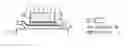
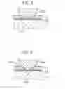
FIG. 1 illustrates a semiconductor device according to the embodiment of the present disclosure. The semiconductor device is utilized for, e.g., a power supply of a TV receiver. Furthermore, FIG. 2 illustrates a planar configuration of the semiconductor device. In FIG. 2, a resin encapsulant is not illustrated. A current ranging from approximately tens of amperes to approximately one hundred amperes flows through the semiconductor device used for the power supply. In order to prevent a corresponding semiconductor element from being damaged due to heat generated by this current, a sufficiently thick copper (Cu) leadframe is used which is formed with a plurality of outer leads 1, a plurality of inner leads 2, a die pad 3, and a heat dissipator 4 as illustrated in FIGS. 1 and 2. The heat dissipator 4 is formed integrally with the side of the die pad 3 furthest from the outer leads 1. Furthermore, the outer leads 1 are formed integrally with the corresponding inner leads 2, and a pair of one of the plurality of outer leads 1 and one of the plurality of inner leads 2 is formed integrally with the die pad 3.
As illustrated in FIG. 2, a semiconductor element (semiconductor chip) 5 is mounted on the die pad 3, and wires 7 made of, e.g., aluminum (Al) provide electrical connection between electrodes 6 formed on the semiconductor element 5 and the corresponding inner leads 2 which are not connected with the die pad 3.
The semiconductor element 5, the wires 7, the inner leads 2, and the die pad 3 are covered with a resin encapsulant 8 (not illustrated in FIG. 2).
The heat dissipator 4 is formed with a screw hole 4a. When a screw is screwed into the screw hole 4a so that the heat dissipator 4 is fixed to a heat dissipation mechanism (not illustrated) of the power supply, heat generated in the semiconductor element 5 can be dissipated to the heat dissipation mechanism through the die pad 3, the heat dissipator 4, and the screw.
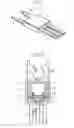
As illustrated in FIG. 3, the semiconductor element 5 is fixed on the die pad 3 by a solder material 9. Specifically, as illustrated in FIG. 4, an approximately 0.1-0.4-μm-thick active layer 10 made of copper, for example, is formed on the surface of the die pad 3 by vacuum deposition, sputtering, or any other method. In this embodiment, the die pad 3 includes the copper active layer 10. Furthermore, although copper is used for the outer leads 1, the inner leads 2, and the die pad 3, a material of the outer leads 1, inner leads 2, and die pad 3 is not limited only to copper. An alloy containing copper and silver (Ag) or cobalt (Co) may be used as the material.
An approximately 1-4-μm-thick first solder bonding layer 11 formed by plating and made of silver (Ag) is provided on the active layer 10. In fabricating a semiconductor device, the die pad 3, the active layer 10, and the first solder bonding layer 11 are treated as a three-layer structure.
A lower portion of the semiconductor element 5 is a semiconductor substrate made of, e.g., silicon (Si). An approximately 0.05-μm-thick adhesion layer 12 made of chrome (Cr), an approximately 0.05-μm-thick intermediate bonding layer 13 made of a nickel (Ni)-chrome (Cr) alloy, and an approximately 0.3-μm-thick barrier layer 14 made of nickel (Ni) are sequentially formed on the lower surface of the semiconductor substrate by vacuum deposition or sputtering. An approximately 0.5-5-μm-thick second solder bonding layer 15 made of silver by vacuum deposition or plating is formed on the lower surface of the barrier layer 14. Specifically, a back electrode 16 for the semiconductor element 5 includes the adhesion layer 12, the intermediate bonding layer 13, the barrier layer 14, and the second solder bonding layer 15.
Although silver is used for the first and second solder bonding layers 11 and 15, a material of these layers is not limited only to silver. An alloy containing silver and cobalt (Co) or copper (Cu) may be used as the material.
Furthermore, the adhesion layer 12 may include an alloy made mostly of chrome. The intermediate bonding layer 13 may include an alloy made mostly of a nickel-chrome alloy. The barrier layer 14 may include an alloy made mostly of nickel.
For the die pad 3 and the semiconductor element 5 which are configured as described above, a solder material 9 is interposed between the first solder bonding layer 11 on the die pad 3 and the second solder bonding layer 15 forming a portion of the back electrode 16 for the semiconductor element 5. Thus, the semiconductor element 5 is mounted on the die pad 3 and fixed thereto by the solder material 9. The reference character 9a illustrated in FIG. 4 denotes floating diffusions of silver diffused from the first and second solder bonding layers 11 and 15 both made of silver into the solder material 9.
As illustrated in FIG. 4, in fabricating a semiconductor device, a recess 11a is formed in the first solder bonding layer 11 by pressing the solder material 9 against the first solder bonding layer 11 because, in this embodiment, the hardness of the solder material 9 is greater than that of the first solder bonding layer 11. Furthermore, an opening 11b is formed in the bottom of the recess 11a to expose the active layer 10 located immediately below the recess 11a, i.e., the die pad 3. As such, the recess 11a is filled with lower part of the solder material 9, and the solder material 9 enters a space located around the opening 11b and between the die pad 3 and the first solder bonding layer 11.
As described above, the semiconductor device according to this embodiment is configured so that the recess 11a is filled with the solder material 9. This increases the bonding area where the first solder bonding layer 11 on the die pad 3 is bonded to the solder material 9, resulting in an increase in the bond strength between the first solder bonding layer 11 and the solder material 9. As a result, the semiconductor element 5 is stably soldered onto the die pad 3.
A method for fabricating a semiconductor device configured as described above will be described hereinafter with reference to the drawings.
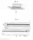
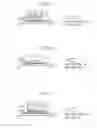
FIGS. 5-11 illustrate a cross-sectional configuration of a semiconductor device in acts of a method for fabricating the semiconductor device according to the first embodiment of the present disclosure in a sequential order.
First, as illustrated in FIG. 5, a die pad 3 having a surface on which an active layer 10 (not illustrated) and a first solder bonding layer 11 have been previously formed is placed on a heat block 17. Thereafter, the die pad 3 is heated to approximately 310° C. in a reducing atmosphere, such as green gas (mixed gas of nitrogen (N2) and hydrogen (H2)), or a non-oxidizing atmosphere, such as a nitrogen (N2) atmosphere.
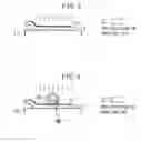
Next, as illustrated in FIG. 6, a spherical solder material 9A is pressed onto the first solder bonding layer 11 on the die pad 3 heated in a reducing or non-oxidizing atmosphere. The solder material 9A is made mostly of bismuth (Bi) and includes copper (Cu), germanium (Ge), and other unavoidable components. The melting point of the solder material 9A is approximately 270° C. Here, the solder material 9A contains approximately 98% bismuth, approximately 2% copper, and approximately 0.06% germanium. Here, weight percentages are denoted by the symbol “%”. Furthermore, the avoidable components include, e.g., steel (Fe), nickel (Ni), lead (Pb), zinc (Zn), aluminum (Al), cadmium (Cd), or arsenic (As). The content of each of the avoidable components contained in the solder material 9A is less than approximately 0.01%.
The Mohs hardness of the solder material 9A is approximately 2.5 which is greater than that of the first solder bonding layer 11 directly below the solder material 9A, i.e., approximately 2.0.
In view of the above, as illustrated in FIG. 7 which is an enlarged view of the region VII in FIG. 6, when the spherical solder material 9A is pressed against the first solder bonding layer 11, a recess 11a is formed in the first solder bonding layer 11, which is softer than the solder material 9A.
As illustrated in FIG. 8, when the solder material 9A is further pressed against the first solder bonding layer 11, an opening 11b is formed in the bottom of the recess 11a. Part of the solder material 9A will soon enter a space between the active layer 10 on the die pad 3 and the first solder bonding layer 11 through the formed opening 11b. Specifically, instead of part of the first solder bonding layer 11 located around the opening 11b, the solder material 9A spreads out to also fill a space located between the active layer 10 and the first solder bonding layer 11 and outside the opening 11b. In this situation, the active layer 10 is bonded to the part of the solder material 9A.
As described above, in this embodiment, lower part of the solder material 9A not only fills the recess 11a, but also is bonded to a wide region of the active layer 10 on the die pad 3 (including a region thereof located outside the opening 11b). This increases the bond strength between the lower part of the solder material 9A and the die pad 3.
The reason why the opening 11b is formed in a part of the first solder bonding layer 11 located under the solder material 9A, and the reason why the solder material 9A spreads out to fill a space outside the opening 11b so that, in this situation, part of the solder material 9A is bonded to the active layer 10 on the die pad 3 are not sufficiently clear yet. However, these reasons will be that, since the solder material 9A is made mostly of bismuth, silver forming the first solder bonding layer 11 has diffused into bismuth. As seen also from the fact that, as illustrated in FIG. 4, silver which has diffused from each of the first and second solder bonding layers 11 and 15 forms a floating diffusion 9a of silver inside the solder material 9, silver will tend to diffuse into bismuth.
Next, as illustrated in FIG. 9, the spherical solder material 9A is spread by a pressure pin 18 with its lower part bonded to the die pad 3 while being heated in a reducing or non-oxidizing atmosphere.
Next, as illustrated in FIG. 10, the solder material 9A is molten so as to be gently raised while being heated in a reducing or non-oxidizing atmosphere.
Next, as illustrated in FIG. 11, a semiconductor element 5 is pressed onto the solder material 9A while being heated in a reducing or non-oxidizing atmosphere. Thereafter, in this situation, the temperature of the solder material 9A is reduced to harden the solder material 9A, thereby obtaining a solder material 9. As a result, a semiconductor device configured as illustrated in FIG. 4 is obtained. The back surface of the semiconductor element 5 is previously formed with a back electrode 16 including an adhesion layer 12, an intermediate bonding layer 13, a barrier layer 14, and a second solder bonding layer 15 which are configured as described above. Furthermore, nickel is used for the barrier layer 14 forming a portion of the back electrode 16. However, since the second solder bonding layer 15 made of silver is interposed between the barrier layer 14 and the solder material 9, nickel ions cannot diffuse into the solder material 9 in the act illustrated in FIG. 11, and therefore the melting temperature of the solder material 9 cannot be increased.
Moreover, the configuration of the back electrode 16 is not limited to the above-described configuration. As long as the back electrode 16 is made of an alloy, such as a gold (Au)-germanium (Ge) alloy, a gold (Au)-germanium (Ge)-antimony (Sb) alloy, or a titanium (Ti)-nickel (Ni)-silver (Ag) alloy, and can be generally used for semiconductor devices, the same advantages can be provided.
As described above, for the semiconductor device of the present disclosure, the first solder bonding layer 11 formed on the surface of the die pad 3 is made of a softer material than the solder material 9 made mostly of bismuth, and the solder material 9 is pressed against the first solder bonding layer 11. Thus, the recess 11a can be formed in a part of the first solder bonding layer 11 so as to be recessed toward the die pad 3. This allows the recess 11a to be filled with the solder material 9. This increases the bonding area where the first solder bonding layer 11 on the die pad 3 is bonded to the solder material 9, resulting in an increase in the bond strength between the solder material 9 and the die pad 3. As a result, the semiconductor element 5 is stably soldered onto the die pad 3.
For the semiconductor device and method for fabricating the same according to the present disclosure, the bond strength between the die pad and the solder material is increased so that the semiconductor element is stably soldered onto the die pad. Therefore, the semiconductor device and method for fabricating the same are useful for semiconductor devices incorporated into electronic devices having high temperatures, in particular, under operating conditions, methods for fabricating the same, etc.
Claims
What is claimed is:1. A semiconductor device comprising:
a die pad having a surface on which a first solder bonding layer is formed, and made of metal; and
a semiconductor element fixed on the first solder bonding layer on the die pad by a solder material made mostly of bismuth,
wherein the first solder bonding layer is made of a softer material than the solder material,
a recess is formed in a part of the first solder bonding layer by pressing the solder material against the first solder bonding layer, and
the solder material partially fills the recess.
2. The semiconductor device of claim 1, wherein
the first solder bonding layer is made of silver or a metal made mostly of silver.
3. The semiconductor device of claim 1, wherein
the solder material contains bismuth, copper, and germanium.
4. The semiconductor device of claim 1, wherein
the die pad is made of copper or a metal made mostly of copper.
5. The semiconductor device of claim 1, wherein
an opening is formed in the recess of the first solder bonding layer to expose the die pad, and
the solder material is in contact with the surface of the die pad through the formed opening.
6. The semiconductor device of claim 5, wherein
the solder material enters a space located around the opening and between the die pad and the first solder bonding layer.
7. The semiconductor device of claim 1, wherein
a second solder bonding layer is formed on a surface of the semiconductor element opposed to the solder material, and the second solder bonding layer is made of silver or a metal made mostly of silver.
8. The semiconductor device of claim 7, wherein
an adhesion layer, an intermediate bonding layer, and a barrier layer are formed between the semiconductor element and the second solder bonding layer sequentially from the semiconductor element toward the second solder bonding layer.
9. The semiconductor device of claim 8, wherein
the adhesion layer is made of chrome, the intermediate bonding layer is made of an alloy of nickel and chrome, and the barrier layer is made of nickel.
10. A method for fabricating the semiconductor device of claim 1, the method comprising acts of:
(a) forming a recess in the first solder bonding layer by pressing the spherical solder material onto the first solder bonding layer formed on the surface of the die pad;
(b) after the act (a), spreading the solder material on the first solder bonding layer; and
(c) after the act (b), pressing the semiconductor element onto the spread solder material.
11. The method of claim 10 further comprising an act of
(d) before the act (a), heating the die pad.
12. The method of claim 10, wherein
in the act (a), an opening is formed in the recess formed in the first solder bonding layer to expose the die pad, and the solder material is in contact with the surface of the die pad through the formed opening.
Images & Drawings included:
Sources:
- United States Patent and Trademark Office - verify current appl. status at the USPTO↗
Similar patent applications:
- » 20120112209
SILICON CARBIDE SUBSTRATE FABRICATION METHOD, SEMICONDUCTOR DEVICE FABRICATION METHOD, SILICON CARBIDE SUBSTRATE, AND SEMICONDUCTOR DEVICE - » 20080315254
Semiconductor device fabrication method, semiconductor device, and semiconductor layer formation method - » 20060043570
Substrate, semiconductor device, substrate fabricating method, and semiconductor device fabricating method - » 20050014377
Semiconductor device fabrication method and semiconductor device fabrication system for minimizing film-thickness variations - » 20080203440
Semiconductor device fabrication method and semiconductor device fabricated thereby - » 20060118952
Micro-hole plating method, gold bump fabrication method and semiconductor device fabrication method using the micro-hole plating method, semiconductor device - » 20060177743
Photomask, photomask fabrication method, and semiconductor device fabrication method - » 20070048890
Semiconductor device fabrication method and semiconductor device - » 20060084251
Plating method, semiconductor device fabrication method and circuit board fabrication method - » 20060084253
Plating method, semiconductor device fabrication method and circuit board fabrication method
Recent applications in this class:
- » 20180230573 2018-08-16
Enhancing mechanical properties of nanostructured materials with interfacial films - » 20180016661 2018-01-18
Bulk metallic glass interference layers - » 20160244863 2016-08-25
Process for manufacturing reclaimed alloy material and process for manufacturing reclaimed amorphous alloy ribbon - » 20160186293 2016-06-30
ZIRCONIUM-BASED AMORPHOUS ALLOY AND METHOD FOR PREPARING THE SAME - » 20160017460 2016-01-21
FREEFALL FORMING OF BULK METALLIC GLASS FEEDSTOCK AND SHEET MATERIAL - » 20150315678 2015-11-05
Methods for constructing parts with improved properties using metallic glass alloys - » 20150307967 2015-10-29
AMORPHOUS ALLOY POWDER FEEDSTOCK PROCESSING - » 20150299825 2015-10-22
Methods for constructing parts using metallic glass alloys, and metallic glass alloy materials for use therewith - » 20150299824 2015-10-22
Amorphous alloy roll forming of feedstock or component part - » 20150159240 2015-06-11
MELT FLUXING METHOD FOR IMPROVED TOUGHNESS AND GLASS-FORMING ABILITY OF METALLIC GLASSES AND GLASS-FORMING ALLOYS
Recent applications for this Assignee:
- » 20250038213 2025-01-30
SLURRY FOR NON-AQUEOUS ELECTROLYTE SECONDARY CELL, METHOD FOR MANUFACTURING SLURRY FOR NON-AQUEOUS ELECTROLYTE SECONDARY CELL, ELECTRODE FOR NON-AQUEOUS ELECTROLYTE SECONDARY CELL, AND NON-AQUEOUS ELECTROLYTE SECONDARY CELL - » 20230388751 2023-11-30
Information providing method and information providing apparatus - » 20230187624 2023-06-15
Positive electrode active material for lithium ion secondary battery and lithium ion secondary battery - » 20220368162 2022-11-17
POWER TRANSMISSION COIL, POWER TRANSMISSION DEVICE, AND UNDERWATER POWER SUPPLY SYSTEMS - » 20220345978 2022-10-27
NETWORK CONTROL DEVICE, NETWORK CONTROL SYSTEM, AND NETWORK CONTROL METHOD - » 20220345847 2022-10-27
Information collecting method, communication control apparatus, and information collector apparatus - » 20220317284 2022-10-06
SURVEILLANCE SYSTEM, AND SURVEILLANCE METHOD - » 20220299596 2022-09-22
MONITORING DEVICE AND MONITORING METHOD - » 20220205908 2022-06-30
Cellulose composite determination method and apparatus for composite resin - » 20220173619 2022-06-02
Power receiver apparatus, power transmission voltage control method, and underwater power supply system