Metal-ceramic substrate
US20100260988A1
2010-10-14
11/990,179
2006-06-02
✅ Patent granted
US 8,435,640 B2
2013-05-07
WO; PCT/DE2006/000951; 20060602
WO; WO2007/016886; 20070215
Vera Katz
Welsh Flaxman & Gitler LLC
2029-01-15
Abstract:
In the case of a metal-ceramic substrate with a multilayered ceramic material in sheet form, and with at least one metallization that is provided on one surface side of the ceramic material and is joined to be ceramic material by direct bonding or active soldering, the ceramic material has at least one inner layer or base layer of a silicon nitride ceramic. The surface side of the ceramic material that is provided with the at least one metallization is formed by an intermediate layer of an oxidic ceramic applied to the base layer.
Assignee:
- CURAMIK ELECTRONICS GMBH 23 🇩🇪 Eschenbach, Germany
Applicant:
Interested in similar patents?
Get notified when new applications in this technology area are published.
Classification:
H05K1/0306 » CPC main
Printed circuits; Details; Use of materials for the substrate Inorganic insulating substrates, e.g. ceramic, glass
H05K1/0306 » CPC main
Printed circuits; Details; Use of materials for the substrate Inorganic insulating substrates, e.g. ceramic, glass
C04B37/021 » CPC further
Joining burned ceramic articles with other burned ceramic articles or other articles by heating with metallic articles in a direct manner, e.g. direct copper bonding [DCB]
C04B37/025 » CPC further
Joining burned ceramic articles with other burned ceramic articles or other articles by heating with metallic articles characterised by the interlayer used consisting of glass or ceramic material
C04B37/026 » CPC further
Joining burned ceramic articles with other burned ceramic articles or other articles by heating with metallic articles characterised by the interlayer used consisting of metals or metal salts
C04B41/90 » CPC further
After-treatment of mortars, concrete, artificial stone or ceramics; Treatment of natural stone of only ceramics; Coating or impregnation for obtaining at least two superposed coatings having different compositions at least one coating being a metal
H01L23/3735 » CPC further
Details of semiconductor or other solid state devices; Arrangements for cooling, heating, ventilating or temperature compensation ; Temperature sensing arrangements; Selection of materials, or shaping, to facilitate cooling or heating, e.g. heatsinks; Cooling facilitated by selection of materials for the device or materials for thermal expansion adaptation, e.g. carbon Laminates or multilayers, e.g. direct bond copper ceramic substrates
H05K3/38 » CPC further
Apparatus or processes for manufacturing printed circuits Improvement of the adhesion between the insulating substrate and the metal
H05K3/38 » CPC further
Apparatus or processes for manufacturing printed circuits Improvement of the adhesion between the insulating substrate and the metal
C04B2111/00844 » CPC further
Mortars, concrete or artificial stone or mixtures to prepare them, characterised by specific function, property or use; Uses not provided for elsewhere in for electronic applications
C04B2235/96 » CPC further
Aspects relating to ceramic starting mixtures or sintered ceramic products; Aspects relating to sintered or melt-casted ceramic products Properties of ceramic products, e.g. mechanical properties such as strength, toughness, wear resistance
C04B2235/9607 » CPC further
Aspects relating to ceramic starting mixtures or sintered ceramic products; Aspects relating to sintered or melt-casted ceramic products; Properties of ceramic products, e.g. mechanical properties such as strength, toughness, wear resistance Thermal properties, e.g. thermal expansion coefficient
C04B2237/062 » CPC further
Aspects relating to ceramic laminates or to joining of ceramic articles with other articles by heating; Aspects relating to interlayers, e.g. used to join ceramic articles with other articles by heating; Ceramic interlayers; Oxidic interlayers based on silica or silicates
C04B2237/064 » CPC further
Aspects relating to ceramic laminates or to joining of ceramic articles with other articles by heating; Aspects relating to interlayers, e.g. used to join ceramic articles with other articles by heating; Ceramic interlayers; Oxidic interlayers based on alumina or aluminates
C04B2237/124 » CPC further
Aspects relating to ceramic laminates or to joining of ceramic articles with other articles by heating; Aspects relating to interlayers, e.g. used to join ceramic articles with other articles by heating; Metallic interlayers based on copper
C04B2237/368 » CPC further
Aspects relating to ceramic laminates or to joining of ceramic articles with other articles by heating; Composition of layers of ceramic laminates or of ceramic or metallic articles to be joined by heating, e.g. Si substrates; Ceramic; Non-oxidic Silicon nitride
C04B2237/407 » CPC further
Aspects relating to ceramic laminates or to joining of ceramic articles with other articles by heating; Composition of layers of ceramic laminates or of ceramic or metallic articles to be joined by heating, e.g. Si substrates; Metallic Copper
C04B2237/58 » CPC further
Aspects relating to ceramic laminates or to joining of ceramic articles with other articles by heating; Processing aspects relating to ceramic laminates or to the joining of ceramic articles with other articles by heating Forming a gradient in composition or in properties across the laminate or the joined articles
C04B2237/704 » CPC further
Aspects relating to ceramic laminates or to joining of ceramic articles with other articles by heating; Processing aspects relating to ceramic laminates or to the joining of ceramic articles with other articles by heating; Forming laminates or joined articles comprising layers of a specific, unusual thickness of one or more of the ceramic layers or articles
C04B2237/706 » CPC further
Aspects relating to ceramic laminates or to joining of ceramic articles with other articles by heating; Processing aspects relating to ceramic laminates or to the joining of ceramic articles with other articles by heating; Forming laminates or joined articles comprising layers of a specific, unusual thickness of one or more of the metallic layers or articles
C04B2237/708 » CPC further
Aspects relating to ceramic laminates or to joining of ceramic articles with other articles by heating; Processing aspects relating to ceramic laminates or to the joining of ceramic articles with other articles by heating; Forming laminates or joined articles comprising layers of a specific, unusual thickness of one or more of the interlayers
H05K2201/0195 » CPC further
Indexing scheme relating to printed circuits covered by; Dielectrics; Dielectric layers Dielectric or adhesive layers comprising a plurality of layers, e.g. in a multilayer structure
H05K2201/0195 » CPC further
Indexing scheme relating to printed circuits covered by; Dielectrics; Dielectric layers Dielectric or adhesive layers comprising a plurality of layers, e.g. in a multilayer structure
H05K2201/0355 » CPC further
Indexing scheme relating to printed circuits covered by; Conductive materials; Structure of the conductor; Layered conductors or foils Metal foils
H05K2201/0355 » CPC further
Indexing scheme relating to printed circuits covered by; Conductive materials; Structure of the conductor; Layered conductors or foils Metal foils
H05K2201/068 » CPC further
Indexing scheme relating to printed circuits covered by; Thermal details wherein the coefficient of thermal expansion is important
H05K2201/068 » CPC further
Indexing scheme relating to printed circuits covered by; Thermal details wherein the coefficient of thermal expansion is important
Y10T428/2495 » CPC further
Stock material or miscellaneous articles; Structurally defined web or sheet [e.g., overall dimension, etc.] including components having same physical characteristic in differing degree Thickness [relative or absolute]
Y10T428/26 » CPC further
Stock material or miscellaneous articles Web or sheet containing structurally defined element or component, the element or component having a specified physical dimension
Y10T428/265 » CPC further
Stock material or miscellaneous articles; Web or sheet containing structurally defined element or component, the element or component having a specified physical dimension; Coating layer not in excess of 5 mils thick or equivalent; Up to 3 mils 1 mil or less
Y10T428/266 » CPC further
Stock material or miscellaneous articles; Web or sheet containing structurally defined element or component, the element or component having a specified physical dimension of base or substrate
C04B41/5037 » CPC further
After-treatment of mortars, concrete, artificial stone or ceramics; Treatment of natural stone; Coating or impregnating e.g. injection in masonry, partial coating of green or fired ceramics, organic coating compositions for adhering together two concrete elements, with inorganic materials with ceramic materials Clay, Kaolin
C04B41/4535 » CPC further
After-treatment of mortars, concrete, artificial stone or ceramics; Treatment of natural stone; Coating or impregnating e.g. injection in masonry, partial coating of green or fired ceramics, organic coating compositions for adhering together two concrete elements, characterised by the method of application applied as a solution, emulsion, dispersion or suspension
C04B41/5024 » CPC further
After-treatment of mortars, concrete, artificial stone or ceramics; Treatment of natural stone; Coating or impregnating e.g. injection in masonry, partial coating of green or fired ceramics, organic coating compositions for adhering together two concrete elements, with inorganic materials Silicates
C04B41/522 » CPC further
After-treatment of mortars, concrete, artificial stone or ceramics; Treatment of natural stone; Coating or impregnating e.g. injection in masonry, partial coating of green or fired ceramics, organic coating compositions for adhering together two concrete elements,; Multiple coating or impregnating multiple coating or impregnating with the same composition or with compositions only differing in the concentration of the constituents, is classified as single coating or impregnation Multiple coatings, for one of the coatings of which at least one alternative is described
C04B41/52 » CPC further
After-treatment of mortars, concrete, artificial stone or ceramics; Treatment of natural stone; Coating or impregnating e.g. injection in masonry, partial coating of green or fired ceramics, organic coating compositions for adhering together two concrete elements, Multiple coating or impregnating multiple coating or impregnating with the same composition or with compositions only differing in the concentration of the constituents, is classified as single coating or impregnation
C04B41/4501 » CPC further
After-treatment of mortars, concrete, artificial stone or ceramics; Treatment of natural stone; Coating or impregnating e.g. injection in masonry, partial coating of green or fired ceramics, organic coating compositions for adhering together two concrete elements, with preformed sheet-like elements
C04B41/5127 » CPC further
After-treatment of mortars, concrete, artificial stone or ceramics; Treatment of natural stone; Coating or impregnating e.g. injection in masonry, partial coating of green or fired ceramics, organic coating compositions for adhering together two concrete elements, with inorganic materials; Metallising, e.g. infiltration of sintered ceramic preforms with molten metal Cu, e.g. Cu-CuO eutectic
C04B41/009 » CPC further
After-treatment of mortars, concrete, artificial stone or ceramics; Treatment of natural stone characterised by the material treated
C04B35/584 » CPC further
Shaped ceramic products characterised by their composition ; Ceramics compositions ; Processing powders of inorganic compounds preparatory to the manufacturing of ceramic products based on non-oxide ceramics based on borides, nitrides, or silicides based on silicon nitride
H01L2924/0002 » CPC further
Indexing scheme for arrangements or methods for connecting or disconnecting semiconductor or solid-state bodies as covered by; Technical content checked by a classifier Not covered by any one of groups , and
H01L2924/00 » CPC further
Indexing scheme for arrangements or methods for connecting or disconnecting semiconductor or solid-state bodies as covered by
C04B37/02 IPC
Joining burned ceramic articles with other burned ceramic articles or other articles by heating with metallic articles
C04B35/622 IPC
Shaped ceramic products characterised by their composition ; Ceramics compositions ; Processing powders of inorganic compounds preparatory to the manufacturing of ceramic products Forming processes; Processing powders of inorganic compounds preparatory to the manufacturing of ceramic products
C04B37/00 IPC
Joining burned ceramic articles with other burned ceramic articles or other articles by heating
B32B18/00 IPC
Layered products essentially comprising ceramics, e.g. refractory products
B32B7/02 IPC
Layered products characterised by the relation between layers; Layered products characterised by the relative orientation of features between layers, or by the relative values of a measurable parameter between layers, i.e. products comprising layers having different physical, chemical or physicochemical properties; Layered products characterised by the interconnection of layers Physical, chemical or physicochemical properties
B32B15/04 IPC
Layered products comprising a layer of metal comprising metal as the main or only constituent of a layer, next to another layer of a
Description
BACKGROUND OF THE INVENTION
The invention relates to a metal-ceramic substrate with a multi-layer, plate-shaped ceramic material and comprising at least one metallization, metal lining, provided on or applied to the surface of the ceramic material, which metallization is bonded to the ceramic material by means of direct bonding (DCB) or active soldering. The ceramic material consists of at least one inner layer or base layer of a silicon nitride ceramic, and the surface of the ceramic material provided with the at least one metallization being formed from an intermediate layer of an oxidic ceramic applied to the at least one base layer.
The invention further relates to a method for manufacturing a metal-ceramic substrate comprising a multi-layer, plate-shaped ceramic material, which consists of at least one inner layer or base layer of a silicon nitride ceramic and comprising at least one metallization provided on a surface of the ceramic material, in which an intermediate layer of an oxidic ceramic is formed on the surface of the ceramic material on the at least one base layer to be provided with the at least one metallization and the at least one metallization is applied to said intermediate layer by direct bonding (DCB) or active soldering of at least one metal layer or foil.
Metal-ceramic substrates or ceramic substrates with metallizations are known in the art, particularly also as circuit boards or substrates for electrical and electronic circuits or modules, especially for high-power circuits or modules.
Also known is the so-called DCB process for the direct bonding with a ceramic material or substrate for manufacturing the metallization required for circuit boards, connections, etc. on a ceramic substrate, e.g. on an aluminum oxide ceramic substrate. In this method, described for example in US-PS 37 44 120 or DE-PS 23 19 854, the surfaces of metal layers or foils, e.g. copper layers or foils are provided with a coating of a chemical compound consisting of the metal, e.g. copper and a reactive gas, preferably oxygen. This coating forms an eutectic or melting layer together with a thin layer of the adjoining metal, with a melting temperature below the melting temperature of the metal, e.g. copper, so that by applying the metal layer or foil to the ceramic and heating all layers, they are bonded together, namely by melting of the metal essentially only in the area of the melting layer or oxide layer. When copper or a copper alloy is used as the metal, this method is also referred to as DCB bonding or the DCB process (direct copper bonding).This DCB process then comprises, for example, the following process steps:
-
- Oxidation of a copper foil so as to produce an even copper oxide layer;
- placing the copper foil on the ceramic layer;
- heating the composite to a process temperature between approx. 1025 and 1083° C., e.g. to approx. 1071° C.;
- cooling to room temperature.
Also known is the so-called active soldering method (DE 22 13 115; EP-A-153 618) for bonding metal layers or metal foils forming metallizations, in particular also of copper layers or copper foils, with the respective ceramic material. In this process, which is used especially for manufacturing a metal-ceramic substrate, a bond is produced at a temperature of ca. 800-1000° C. between a metal foil, for example copper foil, and a ceramic substrate, for example aluminum nitride ceramic, using a hard solder, which in addition to a main component such as copper, silver and/or gold also contains an active metal. This active metal, which is at least one element of the group Hf, Ti, Zr, Nb, Ce, creates a bond between the solder and the ceramic through chemical reaction, while the bond between the solder and the metal is a metallic hard solder bond.
Also known is a metal-ceramic substrate with an inner layer or base layer of a silicon nitride ceramic (EP 798 781) that has a significantly higher mechanical strength as compared with other ceramics, in particular as compared with an aluminum oxide ceramic (Al3O2),. To enable application of the metallizations with the DCB process, it has been suggested to apply an intermediate layer of a pure aluminum oxide ceramic to the base layer of the silicon nitride ceramic. However, this method does not result in a complete bond, and in particular not in a bond without defects or defective spots, between the ceramic material and the metallization. Rather, especially with the use of metallizations of copper, this method results in numerous gas cavities between the metallization and the ceramic material, due to a reaction between the oxygen and the copper or copper oxide eutectic (CU/Cu2O eutectic) and the silicon nitride ceramic, namely corresponding to the following formula:
6 CuO+Si3N4→3 SiO2+6 Cu+N2.
This reaction not only uses up the liquid eutectic Cu/Cu2 phase required for the bonding, but also results in the formation of bubbles due to the gaseous nitrogen (N2). This disadvantageous reaction cannot be avoided by the intermediate layer of pure aluminum oxide ceramic. Based on a finding of the present invention, this is due to the very different thermal expansion coefficients of silicon nitride (3.0×10⁻⁶ K−1) and aluminum oxide (8×10⁻⁶ K−1). These differences in the thermal expansion coefficient causes cracks in the intermediate layer during melting on or sintering of the intermediate layer of the aluminum oxide ceramic, but also during bonding of the metallizations during the DCB process, so that these cracks allow the above-described reaction between the Cu/Cu2O eutectic and the silicon nitride ceramic.
Also known (EP 0 499 589) is a method for providing at least one intermediate layer of pure silicon oxide (SiO2) on a ceramic base layer and then applying the metallization by means of the DCB process. This procedure likewise does not produce usable results, since the eutectic melting required for the DCB process reacts with the SiO2 to form liquid Cu2O—SiO2. An intermediate layer of SiO2 therefore cannot be used for applying the metallizations using the DCB process.
It is an object of the invention is to present a metal-ceramic substrate that retains the basic advantages of the silicon nitride ceramic while preventing the aforementioned disadvantages.
SUMMARY OF THE INVENTION
This object is achieved by a metal-ceramic substrate comprising a multi-layer, plate-shaped ceramic material and comprising at least one metallization provided on the surface of the ceramic material, which (metallization) is bonded to the ceramic material by means of direct bonding (DCB) or active soldering, the ceramic material consisting of at least one inner layer or base layer of a silicon nitride ceramic, and the surface of the ceramic material provided with the at least one metallization being formed from an intermediate layer of an oxidic ceramic applied to the at least one base layer, wherein the at least one intermediate layer of the oxidic ceramic has a thermal expansion coefficient smaller than or not greater than 6×10⁻⁶ K−1, and wherein the free silicon oxide (SiO2) content in the oxidic ceramic forming the at least one intermediate layer is negligible at least in the area of the bond between the intermediate layer and the metallization.
Especially suitable materials for the intermediate layer are forsterite, cordierite, mullite or a combination of at least two of these ceramic materials, possibly also aluminum oxide in combination with forsterite and/or cordierite and/or mullite.
Preferably the oxidic ceramic forming the intermediate layer contains additional sintering additives (e.g. rare earth elements), in addition to further oxidic components, such as LiO2, TiO2, BaO, ZnO, B2O3, CsO, Fe2O3, ZrO2, CuO, Cu2O. Combinations of at least of these components can also be used as oxidic additives, in which case the content of these oxidic additives makes up a maximum of 20 percent by weight of the total mass of the intermediate layer. This oxidic additive makes it possible to precisely control or adjust the properties of the intermediate layer with respect to the fusing temperature. Moreover, the additives make it possible to suppress reactions of the copper oxide (in particular Cu2O) in the DCB process, which can result in fusible reaction products. These rare earth elements in the intermediate layer can also be present due to diffusion of the silicon nitride ceramic base layer during melting of the intermediate layer.
The substrate according to the invention features high adhesive or peel strength of the metallization on the ceramic material. A further significant advantage of the substrate according to the invention is that the ceramic forming the intermediate layer has an elasticity module greater than 300 GPa, so that the oxidic ceramic forming the intermediate layer achieves optimum compensation of the very different thermal expansion coefficients of the silicon nitride ceramic and the metal (e.g. copper) of the metallizations, namely as opposed to the relatively high elasticity module of 390 GPa of aluminum oxide.
In particular, the low elasticity module of the intermediate layer enables metallizations with a high thickness, namely up to three times the thickness of the base layer of the silicon nitride ceramic.
BRIEF DESCRIPTION OF THE DRAWINGS
The invention is explained below in more detail based on exemplary embodiments with reference to the drawings, wherein:
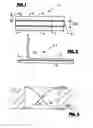
FIG. 1 is a simplified representation of a cross section of a substrate according to the invention;
FIG. 2 is a schematic representation of a method for determining the adhesive or peel strength of a metallization formed by a foil applied to the ceramic material
FIG. 3 is a diagram showing the distribution of free silicon oxide (SiO2) in the intermediate layer of an oxidic ceramic; and
FIG. 4 is a representation similar to FIG. 1 of a further possible embodiment of the substrate according to the invention.
BRIEF DESCRIPTION OF THE INVENTION
The metal-ceramic substrate generally designated 1 in FIG. 1 consists of a plate-shaped ceramic material 2, which is provided on each surface with a metallization 3 and 4 made of a metal foil, i.e. in the depicted embodiment of a copper foil, with a thickness dm applied by means of the DCB process. The ceramic material 2 has a multi-layer design, namely consisting of an inner ceramic or base layer 5 of silicon nitride (Si3N4), which is provided on each side with an intermediate layer 6 and 7 of an oxidic ceramic, so that the application of the metallizations 3 and 4 is possible without defective spots and with high adhesion of the copper forming the metallizations 3 and 4 on the ceramic material 2.
The base layer 5 has a thickness dc and also contains, for example, sintering means in the form of an oxide of Ho, Er, Yb, Y, La, Sc, Pr, Ce, Nd, Dy, Sm and/or Gd. Combinations of one or more of these oxides are also possible as sintering means, in which case Ho2O3 or Er2O3 are primarily used. The content of sintering means in the middle layer is for example between 1 and 8 percent by weight of the total mass of the ceramic forming the base layer 5.
In the depicted embodiment, the two metallizations 3 and 4 have the same thickness dm, which can be a maximum of three times the thickness dc. Normally, the thickness of the metallizations 3 and 4 is between 0.01 and 1 mm. The thickness dc is for example between 0.1 and 2 mm.
The intermediate layers 6 and 7, which are much thinner than the base layer 5 and the metallizations 3 and 4, have a thickness between 0.1 and 10 μm, for example and consist of an oxidic ceramic, which contains no free silicon oxide (SiO2) or in which the content of free SiO2 is negligible at least in the areas of the intermediate layer 6 and 7 adjoining said metallizations.
A suitable material for the intermediate layers 6 and 7 is an oxidic ceramic with a thermal expansion coefficient smaller than or not greater than 6×10⁻⁶ K−1. The following ceramics are particularly suitable for the intermediate layers 6 and 7.
| Forsterite (2MgO—SiO2) | 1.5 × 10⁻⁶ K−1 | |
| Cordierite (2MgO—2Al2O3—5SiO2) | 1.4-2.6 × 10⁻⁶ K−1 | |
| Mullite (3Al2O3—2SiO2) | 4.5-5.3 × 10⁻⁶ K−1 | |
The thermal expansion coefficient of aluminum oxide (Al2O3) on the other hand is 8×10⁻⁶ K−1.
Combinations of one or more of the above oxide ceramics are also suitable for the intermediate layers 6 and 7, in which case the E-module for the intermediate layers is preferably smaller than, but not greater than 300 GPa, in order to achieve a certain compensation of the very different thermal expansion coefficients between the metal or copper of the metallizations 3 and 4 and the Si3N4 of the inner layer 5.
The above materials for the intermediate layers 6 and 7 also enable optimum compliance with said requirement for the expansion behavior or elasticity of the intermediate layers, namely with the use of forsterite, cordierite and mullite and/or a high content of these materials in the respective intermediate layer 6 and 7.
The elasticity modules are as follows:
| Ceramic material | Elasticity module: | |
| Forsterite | 250 GPa | |
| Cordierite | 140 GPa | |
| Mullite | 220 GPa | |
| Aluminum oxide | 390 GPa | |
Preferably the intermediate layers 6 and 7 contain, as described above, one or more additives from the group, LiO2, TiO2, BaO, ZnO, B2O3, CsO, Fe2O3, ZrO2, CuO and/or Cu2O, up to a maximum content of 20 percent by weight of the total mass of the respective intermediate layer.
In the manufacture of the substrate 1, a plate made of the silicon nitride ceramic (Si3N4 ceramic) forming the base layer 5 is used as the starting material. Said plate is then coated on both sides using a suitable process to form the respective intermediate layer 6 and 7 with the suitable ceramic component(s) for the intermediate layer.
Various methods are available for applying this coating, in which for example the ceramic material forming the respective intermediate layer is deposited in combination with a suitable liquid, for example water, on the surfaces of the plate-shaped starting material. Afterwards, after drying, the intermediate layer 6 and 7 is melted on or dense sintered at a temperature between 1200 and 1680° C. in an oxidized atmosphere.
The coating is applied to the starting material for example using microdispersive to nanodispersive mixtures containing the ceramic material, e.g. by spraying, immersion (dip coating or spin coating) of aqueous dispersions; other methods, such as the sol-gel-process can also be used.
After application of the intermediate layers 6 and 7, the metal or copper foils forming the metallizations 3 and 4 are bonded using the known DCB process.
The substrate 1 can be manufactured as a large surface substrate, for example with dimensions greater than 80×80 mm, preferable greater than 100×150 mm, so that the substrate 1, through further processing, i.e. through corresponding structuring of the metallizations 3 and 4, can be used to manufacture a multiple printed panel or multiple substrate, which can then be divided into numerous single substrates.
The substrate 1 with the structure described above features improved mechanical strength, namely due to the base layer 5 of silicon nitride ceramic. Further, the metallizations 3 and 4 can be bonded using the time-tested DCB process with the normal process means, namely without the risk of defective spots in the bond between the metallizations 3 and 4 and the ceramic material 2, which (defective spots) extremely impair the adhesion of the metallizations on the ceramic material and also can impair the dielectric strength of the substrate.
Use of the substrate 1 with the structure described above achieves sufficiently high adhesion of the metallizations on the ceramic material 2. This adhesion or peel strength is measured using the method depicted in FIG. 2. A test sample 1.1, the structure of which corresponds to the substrate 1, however only with the metallization 3 and the intermediate layer 6, is manufactured in the manner described above; the metallization 3 is manufactured as a strip with a width of 1 cm and a thickness dm of 0.3 mm. With the test piece clamped, a force F is applied to the upward extending end 3.1 of the strip-shaped metallization 3, with such intensity that the strip-shaped metallization 3 is pulled off of the ceramic material 1 at a speed of 0.5 cm/min. The force F required for this then defines the adhesion or peel strength, which is greater than 40 N/cm for the substrate 1 as embodied above.
FIG. 3 shows a diagram with the distribution (Curve A) of the free silicon oxide (SiO2) in the intermediate layer 6 or 7, starting from the inner layer 5 to the metallization 3 or 4. As indicated by Curve A, the content of free SiO2 in relation to the content of the oxide ceramic forming the intermediate layer decreases drastically toward the respective metallization 3 or 4, and the content of free SiO2 in the area of the metallization is reduced to 0 percent by weight, in relation to the total mass of the intermediate layer. Curve B in FIG. 3 shows the curve of the content of the oxide ceramic forming the intermediate layer, including the aforementioned additives; the oxide ceramic is mullite, forsterite, cordierite or a combination of one or more of these ceramics.
FIG. 4 shows in a representation similar to FIG. 1, as a further possible embodiment, a substrate 1a, which differs from substrate 1 in that the metallizations 3 and 4 are applied to the ceramic material 2 not by means of the DCB process, but rather by the active soldering process. To achieve this, a layer 8 and 9 of active solder is applied to the surface of the ceramic material, which likewise consists of the base layer 5 of the Si3N4 ceramic and of the two intermediate layers 6 and 7, therefore bonding the respective metallization or the metal or copper foil forming said metallization with the ceramic material 2.
Suitable materials for the active solder are materials that are normally used, e.g. active solder containing a base component or solder component, such as copper/silver, and an active component, such as Ti, Hf or Zr. The manufacture of the substrate 1a is likewise such that the ceramic material 2 is first manufactured in one or more preceding process steps. Afterwards, the metallizations 3 and 4 are applied using the known active soldering process, in which the layers 8 and 9 of active solder are applied either as a paste or a foil.
To manufacture the strip conductors, contacts surfaces, etc., the metal-ceramic substrates are structured in the usual manner, using the usual technology, e.g. the known etch-masking technology.
The invention was described above based on exemplary embodiments. It goes without saying that numerous modifications and variations are possible without abandoning the underlying inventive idea upon which the invention is based.
REFERENCE LIST
- 1, 1a metal-ceramic substrate
- 1.1 test sample
- 2 ceramic material
- 3, 4 metallization
- 5inner layer of silicon nitride ceramic
- 5, 6 intermediate layer of an oxidic ceramic
- 8, 9 active soldering layer
- F pull-off strength
- dc thickness of inner layer of silicon nitride ceramic
- dm thickness of the metal layers forming the metallization
Claims
What is claimed is:1. A metal-ceramic substrate comprising a multi-layer, plate-shaped ceramic material and comprising at least one metallization provided on the a surface of the ceramic material, said at least one metallization is bonded to the ceramic material by means of direct bonding (DCB) or active soldering, the ceramic material comprising at least one inner layer or base layer of a silicon nitride ceramic, and the surface of the ceramic material provided with the at least one metallization being formed from an intermediate layer of an oxidic ceramic applied to the at least one base layer, wherein the at least one intermediate layer of the oxidic ceramic has a thermal expansion coefficient smaller than or not greater than 6×10⁻⁶ K−1, and that the free silicon oxide (SiO2) content in the oxidic ceramic forming the at least one intermediate layer is negligible at least in the area of the bond between the intermediate layer and the metallization.
2. The substrate according to claim 1, wherein the free silicon oxide content in the at least one intermediate layer of the oxidic ceramic is zero or approximately zero at least in the area of the bond between the intermediate layer and the metallization.
3. The substrate according to claim 1, wherein the at least one base layer of the silicon nitride ceramic is provided on each surface with at least one intermediate layer of the oxidic ceramic.
4. The substrate according to claim 3, wherein the at least one metallization is applied to both intermediate layers.
5. The substrate according to claim 1, wherein the ceramic material, with respect to the composite layer and thickness of the ceramic layers, is symmetrical to a center plane extending parallel to the surfaces of the ceramic material.
6. The substrate according to claim 1, wherein with respect to the composite layer or the thickness of the layers, including a thickness of the ceramic layers and of the metallizations, the composite layer is symmetrical to a center plane extending parallel to the surfaces of the substrate.
7. The substrate according to claim 1, wherein the ceramic material used for the at least one intermediate layer has an elasticity module smaller than 300 GPa, an elasticity module between 100 and 300 GPa.
8. The substrate according to claim 1, wherein a thickness of the at least one intermediate layer is significantly smaller than the a thickness (do) of the base layer of the silicon nitride ceramic supporting said intermediate layer is or significantly smaller than the thickness (dm) of the at least one metallization.
9. The substrate according to claim 1, wherein a thickness (dm) of the at least one metallization is not greater than three'times the thickness (do) of the base layer of the silicon nitride ceramic.
10. The substrate according to claim 1, wherein a thickness of the at least one intermediate layer is between 0.1 and 10 μm.
11. The substrate according to claim 1, wherein a thickness (dc) of the at least one base layer of the silicon nitride ceramic is between 0.1 and 2 mm.
12. The substrate according to claim 1, wherein a thickness (dm) of the at least one metallization is between 0.5 and 1 mm.
13. The substrate according to claim 1, the at least one metallization of copper is made of a copper alloy.
14. The substrate according to claim 1, wherein the at least one intermediate layer is forsterite, cordierite, mullite or a mixture or combination of at least two of these components.
15. The substrate according to claim 1, wherein the ceramic of the at least one intermediate layer contains an aluminum oxide ceramic.
16. The substrate according to claim 1, wherein the ceramic of the at least one intermediate layer contains sintering means, in a form of at least one rare earth element.
17. The substrate according to claim 16, wherein the ceramic of the at least one intermediate layer comprises a sintering means an oxide of Ho, Er, Yb, Y, La, Sc, Pr, Ce, Nd, Dy, Sm, Gd or combinations of at least two of these oxides.
18. The substrate according to claim 16 or 17, wherein the content of the sintering means is between 1.0 and 8.0 percent by weight.
19. The substrate according to claim 1, wherein the ceramic of the at least one intermediate layer comprises as an additive at least one oxidic component from the group Li2O, TiO2, BaO, ZnO, B2O3, CsO, Fe2O3, ZrO2, CuO, CU2O, and he a content of said additive makes up a maximum of 20 percent by weight of the total mass of the intermediate layer.
20. The substrate according to claim 1, wherein the at least one layer of the silicon nitride ceramic has a thermal conductivity greater than 45 W/mK.
21. The substrate according to claim 1, wherein an adhesive and peel strength of the at least one metallization on the ceramic material is greater than 40 N/cm.
22. The substrate according to claim 1, wherein at least one layer of an active solder is provided between the at least one intermediate layer and the adjoining metallization.
23. The substrate according to claim 22, wherein the active solder consists of a base component suitable as a solder and an active metal, selected from Ti, Hf, Zr, Nb or Ce.
24. The substrate according to claim 1, wherein outer dimensions of the substrate are greater than 80×80 mm, preferably greater than 100×150 mm.
25. A method for manufacturing a metal-ceramic substrate comprising a multi-layer, plate-shaped ceramic material, which consists of at least one inner layer or base layer of a silicon nitride ceramic and comprising at least one metallization provided on at least one surface of the multi-layer, plate-shaped ceramic material, in which an intermediate layer of an oxidic ceramic is formed on the surface of the ceramic material on the at least one base layer to be provided with the at least one metallization and the at least one metallization is applied to said intermediate layer by direct bonding (DCB) or active soldering of at least one metal layer or foil, wherein an oxidic ceramic is used for the intermediate layer with a thermal expansion coefficient smaller than or not greater than 6×10⁻⁶ K−1 and its free silicon (SiO2) content is negligible at least in the area of the bond between the intermediate layer and the metallization or at the transition between the intermediate layer and the metallization.
26. The method according to claim 25, wherein the intermediate layer is so that the free silicon oxide (SiO2) content is zero or approximately zero in the at least one intermediate layer of the oxidic ceramic, at least in the area of the bond between the intermediate layer and the metallization or at the transition between the intermediate layer and the metallization.
27. The method according to claim 25, wherein the at least one base layer is provided on each surface with an intermediate layer of the oxidic ceramic and at least one metallization is applied to each intermediate layer.
28. The method according to claim 25, wherein the at least one intermediate layer is manufactured with a thickness that is significantly smaller than the thickness (dc) of the base layer the silicon nitride ceramic and/or significantly smaller than the thickness (dm) of the at least one metallization.
29. The method according to claim 25, wherein a metal foil with a thickness (dm) that is a maximum of three times the thickness (dc) of the base layer is used for the at least one metallization.
30. The method according to claim 25, wherein the at least one intermediate layer is manufactured with a thickness between 0.1 and 10 μm.
31. The method according to claim 25, wherein forsterite, cordierite, mullite or of a mixture or combination of at least two of these components is used for the at least one intermediate layer.
32. The method according to claim 25, wherein a ceramic containing an aluminum oxide ceramic is used for the at least one intermediate layer.
33. The method according to claim 25, wherein a ceramic containing at least one sintering means, in the form of at least one rare earth element, is used for the at least one intermediate layer, and that the content of the sintering means is between 1.0 and 8.0 percent by weight.
34. The method according to claim 25, wherein a ceramic containing as an additive at least one oxidic component from the group Li2O, TiO2, BaO, ZnO, B2O3, CsO, Fe2O3, ZrO2, CuO, CU2O is used for the at least one intermediate layer (6, 7), and the content of said additive makes up a maximum of 20 percent by weight of the total mass of the intermediate layer.
35. The method according to claim 25, wherein the base layer is coated on at least one surface with a ceramic material forming the intermediate layer and said coating is melted on or dense sintered at a temperature between 1200 and 1680° C.
36. The method according to claim 35, wherein the melting on or dense sintering takes place in an oxidic atmosphere.
37. The method according to claim 35, wherein the coating is applied by spraying, immersion, of an aqueous dispersion or in a sol-gel process.
38. The method according claim 35, wherein the coating is applied using microdispersive to nanodispersive mixtures containing the ceramic material.
Images & Drawings included:


Sources:
- United States Patent and Trademark Office - verify current appl. status at the USPTO↗
Similar patent applications:
- » 20240139884
METHOD FOR PROCESSING A METAL-CERAMIC SUBSTRATE, AND METAL-CERAMIC SUBSTRATE - » 20240178098
METHOD FOR PRODUCING A METAL-CERAMIC SUBSTRATE, AND METAL-CERAMIC SUBSTRATE PRODUCED USING A METHOD OF THIS TYPE - » 20200361828
Method for producing a semi-finished metal product, method for producing a metal-ceramic substrate, and metal-ceramic substrate - » 20230294213
METHOD FOR PRODUCING A METAL-CERAMIC SUBSTRATE, AND METAL-CERAMIC SUBSTRATE PRODUCED USING A METHOD OF THIS TYPE - » 20210233828
System for cooling a metal-ceramic substrate, a metal-ceramic substrate and method for manufacturing the system - » 20220295641
Method for producing a metal-ceramic substrate, and metal-ceramic substrate produced using such a method - » 10416540
PROCESS FOR THE MANUFACTURE OF METAL-CERAMIC COMPOUND MATERIAL IN PARTICULAR METAL-CERAMIC SUBSTRATES AND METAL-CERAMIC COMPOUND MATERIAL ESPECIALLY METAL-CERAMIC SUBSTRATE MANUFACTURED ACCORDING TO THIS PROCESS - » 20230164913
Process for Producing a Metal-Ceramic Substrate, and a Metal-Ceramic Substrate Produced Using Such Method - » 20230286872
PROCESS FOR PRODUCING A METAL-CERAMIC SUBSTRATE, AND A METAL-CERAMIC SUBSTRATE PRODUCED USING SUCH A METHOD - » 20220362891
Method for producing a metal-ceramic substrate, solder system, and metal-ceramic substrate produced using such a method
Recent applications in this class:
- » 20250294675 2025-09-18
DOUBLE-SIDE ACTIVE METAL BRAZING SUBSTRATE AND METHOD FOR MANUFACTURING THE SAME - » 20250287498 2025-09-11
PRINTED CIRCUIT BOARD - » 20250267788 2025-08-21
GLASS CORE LAMINATE, GLASS CORE LAMINATE MANUFACTURING METHOD, AND GLASS CORE LAMINATE CUTTING METHOD - » 20250261305 2025-08-14
GLASS SUBSTRATE, MULTILAYER WIRING SUBSTRATE, AND METHOD FOR PRODUCING GLASS SUBSTRATE - » 20250240884 2025-07-24
METAL-CERAMIC SUBSTRATE WITH CONTACT AREA - » 20250234456 2025-07-17
PREPREG, LAMINATE, AND PRODUCTION METHODS THEREFOR, AS WELL AS PRINTED CIRCUIT BOARD AND SEMICONDUCTOR PACKAGE - » 20250212324 2025-06-26
WIRING BOARD - » 20250203769 2025-06-19
WIRING SUBSTRATE AND MANUFACTURING METHOD THEREOF - » 20250203768 2025-06-19
CERAMIC WIRING BOARD, ELECTRONIC DEVICE, AND ELECTRONIC MODULE - » 20250194004 2025-06-12
PRINTED CIRCUIT BOARD
Recent applications for this Assignee:
- » 20140166533 2014-06-19
Packaging for substrates and packaging unit having such packaging - » 20130213853 2013-08-22
Package for metal-ceramic substrate and method for packing such substrates - » 20120193324 2012-08-02
Method for the production of a metal-ceramic substrate, preferably a copper ceramic substrate - » 20120134115 2012-05-31
Electronic device - » 20120045657 2012-02-23
Metal-Ceramic Substrate - » 20120031653 2012-02-09
Printed circuit board made from a composite material - » 20100290490 2010-11-18
Heat sink and assembly or module unit - » 20100227114 2010-09-09
Composite material, especially multilayer material, and adhesive or bonding material - » 20090272417 2009-11-05
Process for producing Peltier modules, and Peltier module - » 20090232972 2009-09-17
Method for the production of a metal-ceramic substrate