Flexible underfill compositions for enhanced reliability
US20120074597A1
2012-03-29
12/890,545
2010-09-24
✅ Patent granted
US 9,068,067 B2
2015-06-30
-
-
Peter F Godenschwager | David Karst
Konrad Raynes Davda & Victor LLP | Alan S. Raynes
2033-11-12
Abstract:
Underfill materials for fabricating electronic devices are described. One embodiment includes an underfill composition including an epoxy mixture, an amine hardener component, and a filler. The epoxy mixture may include a first epoxy comprising a bisphenol epoxy, a second epoxy comprising a multifunctional epoxy, and a third epoxy comprising an aliphatic epoxy, the aliphatic epoxy comprising a silicone epoxy. The first, second, and third epoxies each have a different chemical structure. Other embodiments are described and claimed.
Inventors:
- Dingying Xu 12 🇺🇸 Maricopa, AZ, United States
- Nachiket Raravikar 9 🇺🇸 Gilbert, AZ, United States
- Rahul N. Manepalli 101 🇺🇸 Chandler, AZ, United States
- Nisha Ananthakrishnan 35 🇺🇸 Chandler, AZ, United States
- Hong Dong 6 🇺🇸 Perry Hall, MD, United States
- Gregory S. CONSTABLE 9 🇺🇸 Chandler, AZ, United States
Assignee:
- INTEL CORPORATION 47,158 🇺🇸 Santa Clara, CA, United States
Applicant:
Interested in similar patents?
Get notified when new applications in this technology area are published.
Classification:
C08G59/02 » CPC main
Polycondensates containing more than one epoxy group per molecule ; Macromolecules obtained by polymerising compounds containing more than one epoxy group per molecule using curing agents or catalysts which react with the epoxy groups Polycondensates containing more than one epoxy group per molecule
C07F7/0838 » CPC further
Compounds containing elements of Groups 4 or 14 of the Periodic System; Silicon compounds; Compounds having one or more C—Si linkages; Compounds having one or more O-Si linkage Compounds with one or more Si-O-Si sequences
H01L2224/05573 » CPC further
Indexing scheme for arrangements for connecting or disconnecting semiconductor or solid-state bodies and methods related thereto as covered by; Means for bonding being attached to, or being formed on, the surface to be connected, e.g. chip-to-package, die-attach, "first-level" interconnects; Manufacturing methods related thereto; Bonding areas; Manufacturing methods related thereto; Structure, shape, material or disposition of the bonding areas prior to the connecting process of an individual bonding area; External layer Single external layer
Y10T428/31515 » CPC further
Stock material or miscellaneous articles; Composite [nonstructural laminate]; Of epoxy ether As intermediate layer
H01L2924/14 » CPC further
Indexing scheme for arrangements or methods for connecting or disconnecting semiconductor or solid-state bodies as covered by; Details of semiconductor or other solid state devices to be connected; Device type Integrated circuits
H01L2924/00 » CPC further
Indexing scheme for arrangements or methods for connecting or disconnecting semiconductor or solid-state bodies as covered by
H01L2924/00014 » CPC further
Indexing scheme for arrangements or methods for connecting or disconnecting semiconductor or solid-state bodies as covered by; Technical content checked by a classifier the subject-matter covered by the group, the symbol of which is combined with the symbol of this group, being disclosed without further technical details
H01L2224/05599 » CPC further
Indexing scheme for arrangements for connecting or disconnecting semiconductor or solid-state bodies and methods related thereto as covered by; Means for bonding being attached to, or being formed on, the surface to be connected, e.g. chip-to-package, die-attach, "first-level" interconnects; Manufacturing methods related thereto; Bonding areas; Manufacturing methods related thereto; Structure, shape, material or disposition of the bonding areas prior to the connecting process of an individual bonding area; External layer Material
H01L23/48 IPC
Details of semiconductor or other solid state devices Arrangements for conducting electric current to or from the solid state body in operation, e.g. leads, terminal arrangements ; Selection of materials therefor
C08L23/0884 » CPC main
Compositions of homopolymers or copolymers of unsaturated aliphatic hydrocarbons having only one carbon-to-carbon double bond; Compositions of derivatives of such polymers not modified by chemical after-treatment; Homopolymers or copolymers of ethene; Copolymers of ethene; Copolymers of ethene with unsaturated hydrocarbons containing other atoms than carbon or hydrogen atoms; Acids or derivatives thereof Epoxide containing esters
H01L21/563 » CPC further
Processes or apparatus adapted for the manufacture or treatment of semiconductor or solid state devices or of parts thereof; Manufacture or treatment of semiconductor devices or of parts thereof the devices having at least one potential-jump barrier or surface barrier, e.g. PN junction, depletion layer or carrier concentration layer; Assembly of semiconductor devices using processes or apparatus not provided for in a single one of the subgroups - , e.g. sealing of a cap to a base of a container; Encapsulations, e.g. encapsulation layers, coatings Encapsulation of active face of flip-chip device, e.g. underfilling or underencapsulation of flip-chip, encapsulation preform on chip or mounting substrate
H01L23/293 » CPC further
Details of semiconductor or other solid state devices; Encapsulations, e.g. encapsulating layers, coatings, e.g. for protection characterised by the material, e.g. carbon Organic, e.g. plastic
H01L24/16 » CPC further
Arrangements for connecting or disconnecting semiconductor or solid-state bodies; Methods or apparatus related thereto; Means for bonding being attached to, or being formed on, the surface to be connected, e.g. chip-to-package, die-attach, "first-level" interconnects; Manufacturing methods related thereto; Bump connectors ; Manufacturing methods related thereto; Structure, shape, material or disposition of the bump connectors after the connecting process of an individual bump connector
H01L24/73 » CPC further
Arrangements for connecting or disconnecting semiconductor or solid-state bodies; Methods or apparatus related thereto Means for bonding being of different types provided for in two or more of groups , , , , , , ,
H01L24/92 » CPC further
Arrangements for connecting or disconnecting semiconductor or solid-state bodies; Methods or apparatus related thereto; Methods for connecting semiconductor or solid state bodies including different methods provided for in two or more of groups - Specific sequence of method steps
H01L2224/73204 » CPC further
Indexing scheme for arrangements for connecting or disconnecting semiconductor or solid-state bodies and methods related thereto as covered by; Means for bonding being of different types provided for in two or more of groups; Location after the connecting process on the same surface; Bump and layer connectors the bump connector being embedded into the layer connector
H01L2224/92125 » CPC further
Indexing scheme for arrangements for connecting or disconnecting semiconductor or solid-state bodies and methods related thereto as covered by; Methods for connecting semiconductor or solid state bodies including different methods provided for in two or more of groups - ; Specific sequence of method steps; Connecting a surface with connectors of different types; Sequential connecting processes the first connecting process involving a bump connector the second connecting process involving a layer connector
H01L2924/15311 » CPC further
Indexing scheme for arrangements or methods for connecting or disconnecting semiconductor or solid-state bodies as covered by; Details of package parts other than the semiconductor or other solid state devices to be connected; Die mounting substrate; Connection portion the connection portion being formed only on the surface of the substrate opposite to the die mounting surface being a ball array, e.g. BGA
H01L2924/3512 » CPC further
Indexing scheme for arrangements or methods for connecting or disconnecting semiconductor or solid-state bodies as covered by; Technical effects; Mechanical effects; Thermal stress Cracking
C08G59/3254 » CPC further
Polycondensates containing more than one epoxy group per molecule ; Macromolecules obtained by polymerising compounds containing more than one epoxy group per molecule using curing agents or catalysts which react with the epoxy groups; Macromolecules obtained by polymerising compounds containing more than one epoxy group per molecule using curing agents or catalysts which react with the epoxy groups ; e.g. general methods of curing characterised by the epoxy compounds used; Epoxy compounds containing three or more epoxy groups containing atoms other than carbon, hydrogen, oxygen or nitrogen
C08G59/38 » CPC further
Polycondensates containing more than one epoxy group per molecule ; Macromolecules obtained by polymerising compounds containing more than one epoxy group per molecule using curing agents or catalysts which react with the epoxy groups; Macromolecules obtained by polymerising compounds containing more than one epoxy group per molecule using curing agents or catalysts which react with the epoxy groups ; e.g. general methods of curing characterised by the epoxy compounds used; Epoxy compounds containing three or more epoxy groups together with di-epoxy compounds
C04B41/49 IPC
After-treatment of mortars, concrete, artificial stone or ceramics; Treatment of natural stone; Coating or impregnating e.g. injection in masonry, partial coating of green or fired ceramics, organic coating compositions for adhering together two concrete elements, with organic materials Compounds having one or more carbon-to-metal or carbon-to-silicon linkages Organo-clay compounds; Organo-silicates, i.e. ortho- or polysilicic acid esters ; Organo-phosphorus compounds; Organo-inorganic complexes
C08L83/00 IPC
Compositions of macromolecular compounds obtained by reactions forming in the main chain of the macromolecule a linkage containing silicon with or without sulfur, nitrogen, oxygen or carbon only; Compositions of derivatives of such polymers
C08G77/00 IPC
Macromolecular compounds obtained by reactions forming a linkage containing silicon with or without sulfur, nitrogen, oxygen or carbon in the main chain of the macromolecule
C08L63/00 IPC
Compositions of epoxy resins; Compositions of derivatives of epoxy resins
C08G65/48 IPC
Macromolecular compounds obtained by reactions forming an ether link in the main chain of the macromolecule from hydroxy compounds or their metallic derivatives Polymers modified by chemical after-treatment
C08L23/08 IPC
Compositions of homopolymers or copolymers of unsaturated aliphatic hydrocarbons having only one carbon-to-carbon double bond; Compositions of derivatives of such polymers not modified by chemical after-treatment; Homopolymers or copolymers of ethene Copolymers of ethene
H01L21/56 IPC
Processes or apparatus adapted for the manufacture or treatment of semiconductor or solid state devices or of parts thereof; Manufacture or treatment of semiconductor devices or of parts thereof the devices having at least one potential-jump barrier or surface barrier, e.g. PN junction, depletion layer or carrier concentration layer; Assembly of semiconductor devices using processes or apparatus not provided for in a single one of the subgroups - , e.g. sealing of a cap to a base of a container Encapsulations, e.g. encapsulation layers, coatings
H01L23/29 IPC
Details of semiconductor or other solid state devices; Encapsulations, e.g. encapsulating layers, coatings, e.g. for protection characterised by the material, e.g. carbon
C08G59/32 IPC
Polycondensates containing more than one epoxy group per molecule ; Macromolecules obtained by polymerising compounds containing more than one epoxy group per molecule using curing agents or catalysts which react with the epoxy groups; Macromolecules obtained by polymerising compounds containing more than one epoxy group per molecule using curing agents or catalysts which react with the epoxy groups ; e.g. general methods of curing characterised by the epoxy compounds used Epoxy compounds containing three or more epoxy groups
H01L23/00 IPC
Details of semiconductor or other solid state devices
Description
RELATED ART
In certain conventional electronic assembly manufacturing procedures, a die and a package substrate are brought into electrical contact with one another using solder bumps. A reflow operation is carried out by heating to a temperature greater than the melting point of the solder, and a solder connection is made between the pads on the die and pads on the substrate. A gap remains between the die and the substrate. A material such as a polymer is then typically placed into the gap between the chip and substrate, as an underfill encapsulant. One example of a package substrate is known as a ball grid array (BGA). BGA packages have a plurality of solder bumps located on an opposite surface that the die is attached to. Another reflow operation is carried out by heating to a temperature greater than the melting point of the solder bumps on the BGA package, and a solder connection is made between the package substrate and the board.
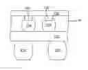
FIG. 1 illustrates certain features of one conventional assembly manufacturing process. As illustrated in FIG. 1, a dispenser 16 such as a needle is positioned adjacent to a die 10 coupled to a package substrate 12 through solder bumps 14. An underfill material 18 is dispensed on the substrate 12 next to the die attach area. The underfill material 18 may comprise, for example, an epoxy mixture, one or more hardeners, a toughening agent, an adhesion promoter or coupling agent, and a filler. With the application of heat, the underfill material 18 may be made to flow between the die 10 and substrate 12, using capillary action. The underfill material 18 may then be cured by heating the assembly to a temperature of, for example, about 150° C. The cured underfill material 18 surrounds the solder bumps 14 and protects the bumps and connection between the die 10 and substrate 12, as well as assist in supporting the die 10 on the substrate 12. The underfill may also act to distribute stresses such as coefficient of thermal expansion (CTE) mismatch-induced stresses over the entire surface. Such CTE mismatch-induced stresses may be generated during the repeated heat cycles during the various processing operations. In addition, the underfill may act to inhibit moisture and other contamination from reaching the interconnection region between the die and substrate.
BRIEF DESCRIPTION OF THE DRAWINGS
Embodiments are described by way of example, with reference to the accompanying drawings, which are not drawn to scale, wherein:
FIG. 1 illustrates a side cross-sectional view of a conventional processing operation in which an underfill material is dispensed on a package substrate;
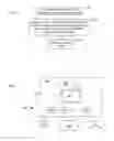
FIG. 2 illustrates a view of a portion of an assembly including a die coupled to a BGA substrate, with an underfill material positioned between the die and substrate, in accordance with certain embodiments;
FIG. 3 illustrates a flow chart of operations in a process for forming an assembly using an underfill material, in accordance with certain embodiments; and
FIG. 4 illustrates an electronic system arrangement in which embodiments may find application.
DETAILED DESCRIPTION
Certain embodiments relate to underfill materials and their use in the formation of electronic assemblies.
Conventional underfill compositions have been found to suffer from electrical failures brought on by propagation of underfill sidewall delamination and underfill cracking in reliability tests. In addition, the volatility of certain aliphatic epoxies and hardener materials used in conventional underfill compositions lead to reactions that form outgassing of undesirable intermediates, which may contaminate the processing equipment or cause other environmental problems. For example, a reaction between an amine hardener and an aliphatic epoxy in the presence of heat, during a curing process, may result in the formation of an undesirable polymer intermediate, as set forth in the reaction process example below:
Reaction Process Example 1
Such a polymer intermediate may stain processing equipment and walls.
Certain embodiments relate to underfill compositions that are formulated to inhibit the formation of intermediates that contaminate the environment, as well as reduce the occurrence of electrical failures of large die BGA packages caused by underfill fillet cracking, and improve reliability.
In certain embodiments, a conventional aliphatic epoxy such as that set forth in the reaction process example 1 is replaced with an aliphatic epoxy component having a different chemical structure. Such a different aliphatic epoxy may, in certain embodiments, be selected from silicone epoxy and glycol epoxy structures.
An underfill composition in accordance with one such group of embodiments includes the use of a silicone epoxy together with other epoxies. Such other epoxies may include a variety of suitable bisphenol epoxies and multifunctional epoxies. Multifunctional epoxies include two or more epoxide groups for the purposes of crosslinking. In one embodiment, the underfill includes a plurality of constituents, including first, second, and third epoxies, the epoxies having different chemical structures, the first epoxy a bisphenol F (bis-F) epoxy, the second epoxy a multifunctional epoxy, and the third epoxy a linear silicone epoxy. In certain embodiments, the silicone epoxy may have the following structure, wherein R is selected from the group consisting of methyl (CH3) and ethyl (C2H5) groups:
In one specific embodiment, each R is a methyl group (CH3) and the structure has the chemical formula C16H34O5Si2. In other embodiments, there may be some R sites with a methyl group and some R sites with an ethyl group.
It is believed that the addition of the linear silicone epoxy into the epoxy matrix, in accordance with certain embodiments, results in an increased matrix ductility and toughness of the underfill.
Another embodiment including a silicone epoxy includes a linear epoxy containing a flexible substituted silicone structure, for example, the structure set forth below, where R is selected from the group consisting of methyl and ethyl groups:
In one specific embodiment, each R is a methyl group (CH3) and the structure has the chemical formula C23H43O6Si3. In other embodiments, there may be some R sites with a methyl group and some R sites with an ethyl group.
An underfill composition in accordance with another group of embodiments includes the use of a glycol epoxy together with other epoxies. Such other epoxies may include a variety of suitable bisphenol epoxies and multifunctional epoxies. In one embodiment, the underfill includes a plurality of constituents, including first, second, and third epoxies, the first epoxy a bis-F epoxy, the second epoxy a multifunctional epoxy, and the third epoxy selected from a linear polypropylene glycol epoxy or a linear polyethylene glycol epoxy. One embodiment includes a polypropylene glycol epoxy having the following structure:
where n is in the range of 3 to 9. One specific embodiment includes n equal to 9. The polypropylene glycol epoxy with n equal to 9 is available from Dow Chemical Co., as D.E.R.™ 732 liquid epoxy resin.
Another embodiment includes a polyethylene glycol epoxy having the following structure:
where n is in the range of 6 to 12.
It is believed that the addition of the linear polypropylene or polyethylene glycol epoxy into the epoxy matrix results in an increased matrix ductility and toughness of the underfill.
In addition to the epoxy components described above, underfill embodiments may also include one or more of certain other suitable components, including, but not limited to, hardening agents, tougheners, adhesion promoters, and fillers. An example of a hardening agent is the amine set forth in the reaction process example 1 set forth above. A filler (for example, SiO2) may in certain embodiments be present in an amount of about 50-70 weight percent.
FIG. 2 illustrates a cross-sectional view of an electronic assembly, in accordance with certain embodiments. As seen in FIG. 2, an underfill material 118 is placed into a region between a body such as a die 110 and a body such as a BGA substrate 112. The die 110 may include a plurality of bonding pads 124 thereon. The die 110 is electrically coupled to regions on the BGA substrate 112 through solder 114 that is in contact with the bonding pads 124. The BGA substrate 112 may include a plurality of solder bumps 214 for coupling to a board, as well as other features such as bonding pads (not shown). The underfill material 118 may include an epoxy mixture such as those described in certain embodiments above, including a bisphenol epoxy, a multi-functional epoxy, and an epoxy selected from the group consisting of a silicone epoxies and glycol epoxies. Other materials such as fillers and additives may also be present in the underfill material 118. Once the under material 118 is properly positioned, it may be cured.
FIG. 3 is a flow chart showing a number of operations in accordance with certain embodiments. Box 300 is electrically coupling a first body (for example, a die), to a second body (for example, a package substrate), using a method such as, for example, a C4 (controlled collapse chip connection) process, in which a gap remains between the first body and the second body. Solder bumps may be used to make the electrical connection between the first body and the second body. Box 302 is positioning an underfill material including an epoxy mixture, including a bisphenol epoxy, a multifunctional epoxy, and an epoxy selected from silicone epoxies and glycol epoxies, between the first body and the second body. Box 304 is applying heat to cure the underfill. Various additions and/or modifications may be made to the above operations where suitable.
Embodiments such as described above may have one or more of the following advantages, including: (1) providing enhanced resistance to cracking as compared with conventional underfill compositions; and (2) reducing volatile outgassing and contamination during processing due to the use of less volatile epoxy mixture.
Assemblies including, for example, a package substrate and die joined together as described in embodiments above may find application in a variety of electronic components, at various interconnection levels within the assembly. FIG. 4 schematically illustrates one example of an electronic system environment in which aspects of described embodiments may be embodied. Other embodiments need not include all of the features specified in FIG. 4, and may include alternative features not specified in FIG. 4.
The system 401 of FIG. 4 may include at least one central processing unit (CPU) 403. The CPU 403, also referred to as a microprocessor, may be a die which is attached to an integrated circuit package substrate 405, which is then coupled to a printed circuit board 407, which in this embodiment, may be a motherboard. The CPU 403 on the package substrate 405 is an example of an electronic device assembly that may be formed in accordance with embodiments such as described above, including an underfill material comprising the epoxy mixtures described above. A variety of other system components, including, but not limited to memory and other components discussed below, may also include die and substrate structures formed in accordance with the embodiments described above.
The system 401 may further include memory 409 and one or more controllers 411a, 411b . . . 411n, which are also disposed on the motherboard 407. The motherboard 407 may be a single layer or multi-layered board which has a plurality of conductive lines that provide communication between the circuits in the package 405 and other components mounted to the board 407. Alternatively, one or more of the CPU 403, memory 409 and controllers 411a, 411b . . . 411n may be disposed on other cards such as daughter cards or expansion cards. The CPU 403, memory 409 and controllers 411a, 411b . . . 411n may each be seated in individual sockets or may be connected directly to a printed circuit board. A display 415 may also be included.
Any suitable operating system and various applications execute on the CPU 403 and reside in the memory 409. The content residing in memory 409 may be cached in accordance with known caching techniques. Programs and data in memory 409 may be swapped into storage 413 as part of memory management operations. The system 401 may comprise any suitable computing device, including, but not limited to, a mainframe, server, personal computer, workstation, laptop, handheld computer, handheld gaming device, handheld entertainment device (for example, MP3 (moving picture experts group layer-3 audio) player), PDA (personal digital assistant) telephony device (wireless or wired), network appliance, virtualization device, storage controller, network controller, router, etc.
The controllers 411a, 411b . . . 411n may include one or more of a system controller, peripheral controller, memory controller, hub controller, I/O (input/output) bus controller, video controller, network controller, storage controller, communications controller, etc. For example, a storage controller can control the reading of data from and the writing of data to the storage 413 in accordance with a storage protocol layer. The storage protocol of the layer may be any of a number of known storage protocols. Data being written to or read from the storage 413 may be cached in accordance with known caching techniques. A network controller can include one or more protocol layers to send and receive network packets to and from remote devices over a network 417. The network 417 may comprise a Local Area Network (LAN), the Internet, a Wide Area Network (WAN), Storage Area Network (SAN), etc. Embodiments may be configured to transmit and receive data over a wireless network or connection. In certain embodiments, the network controller and various protocol layers may employ the Ethernet protocol over unshielded twisted pair cable, token ring protocol, Fibre Channel protocol, etc., or any other suitable network communication protocol.
The terms “a” and “an” as used herein denote the presence of at least one of the referenced item, and do not denote a limitation of quantity. In addition, terms such as “first”, “second”, and the like as used herein to not necessarily denote any particular order, quantity, or importance, but are used to distinguish one element from another.
While certain exemplary embodiments have been described above and shown in the accompanying drawings, it is to be understood that such embodiments are merely illustrative and not restrictive, and that embodiments are not restricted to the specific constructions and arrangements shown and described since modifications may occur to those having ordinary skill in the art.
Claims
What is claimed:1. An underfill composition comprising:
an epoxy mixture comprising a first epoxy comprising a bisphenol epoxy, a second epoxy comprising a multifunctional epoxy, and a third epoxy comprising an aliphatic epoxy, the aliphatic epoxy comprising a silicone epoxy; the first, second, and third epoxies each having a different chemical structure;
an amine hardener component; and
a filler.
2. The underfill composition of claim 1, wherein the silicone epoxy has the chemical formula C16H34O5Si2.
3. The underfill composition of claim 1, wherein the silicone epoxy has the following structure:
where R is a group selected from the group consisting of methyl and ethyl groups.
4. The underfill composition of claim 1, wherein the silicone epoxy comprises a linear epoxy containing a flexible substituted silicone structure.
5. The underfill composition of claim 1, wherein the bisphenol epoxy comprises a bisphenol F epoxy.
6. The underfill composition of claim 1, wherein the silicone epoxy has the following structure:
where R is a group selected from the group consisting of methyl groups and ethyl groups.
7. The underfill composition of claim 6, wherein the silicone epoxy has the chemical formula C23H43O6Si3.
8. An underfill composition comprising:
an epoxy mixture comprising a first epoxy comprising a bisphenol epoxy, a second epoxy comprising a multifunctional epoxy, and a third epoxy comprising an aliphatic epoxy, the aliphatic epoxy comprising a glycol epoxy; the first, second, and third epoxies each having a different chemical structure;
an amine hardener component; and
a filler.
9. The underfill composition of claim 8, wherein the glycol epoxy comprises a polypropylene glycol epoxy.
10. The underfill composition of claim 9, wherein the polypropylene glycol epoxy has the following structure:
where n equals 3 to 9.
11. The underfill composition of claim 10, where n equals 9.
12. The underfill composition of claim 8, wherein the glycol epoxy comprises a polyethylene glycol epoxy.
13. The underfill composition of claim 11, wherein the polyethylene glycol epoxy has the following structure:
where n equals 6 to 12.
14. The underfill composition of claim 8, wherein the bisphenol epoxy comprises a bisphenol F epoxy.
15. An assembly comprising:
a die;
a substrate;
the die electrically coupled to the substrate;
a gap between the die and the substrate;
an underfill material in the gap, the underfill material comprising first, second, and third epoxies, each having a different chemical structure, the first epoxy comprising a bisphenol epoxy, the second epoxy comprising a multifunctional epoxy, and the third epoxy comprising an aliphatic epoxy selected from the group consisting of silicone epoxies and glycol epoxies.
16. The assembly of claim 15, wherein the underfill material further comprises an amine hardener and a filler.
17. The assembly of claim 15, wherein the third epoxy comprises a linear silicone epoxy.
18. The assembly of claim 15, wherein the third epoxy comprises a glycol epoxy selected from the group consisting of polypropylene glycol epoxy and polyethylene glycol epoxy.
19. The underfill composition of claim 14, wherein the bisphenol epoxy comprises a bisphenol F epoxy.
Images & Drawings included:


Sources:
- United States Patent and Trademark Office - verify current appl. status at the USPTO↗
Similar patent applications:
Recent applications in this class:
- » 20240043605 2024-02-08
CURABLE COMPOSITION - » 20230203236 2023-06-29
LIQUID COMPRESSION MOLDING MATERIAL - » 20230183414 2023-06-15
CURABLE EPOXY COMPOSITION FOR ROTARY ELECTRIC MACHINE - » 20220002470 2022-01-06
Method of lining a structure with a delayed curing resin composition - » 20190352447 2019-11-21
Delayed curing resin composition - » 20180346638 2018-12-06
Delayed curing resin composition - » 20180179328 2018-06-28
Delayed curing resin composition - » 20170275413 2017-09-28
Epoxy resin composition for casting - » 20160237200 2016-08-18
Curable resin composition, article, and method for fabricating the same - » 20160185895 2016-06-30
Resin composition and coating material using the same
Recent applications for this Assignee:
- » 20250294866 2025-09-18
GATE CUT CONFINED WITHIN GATE TRENCH - » 20250294846 2025-09-18
BACKSIDE CROSS-COUPLE INTERCONNECTS - » 20250294835 2025-09-18
ELONGATED VERTICAL STRUCTURES OF CHANNEL MATERIALS - » 20250294827 2025-09-18
CO-INTEGRATION OF GATE-ALL-AROUND DEVICES WITH DIFFERENT NUMBERS OF NANORIBBONS - » 20250294818 2025-09-18
TRANSISTOR DESIGNS FOR FLOATING BODY MEMORY - » 20250294781 2025-09-18
MAGNETIC CORE INDUCTORS ON PACKAGE SUBSTRATES - » 20250294777 2025-09-18
INTEGRATED CIRCUIT DEVICE WITH MEMORY ARRAY AND SHARED GAIN ELEMENT - » 20250293985 2025-09-18
RECEIVER-BASED PRECISION CONGESTION CONTROL - » 20250293860 2025-09-18
PRESERVATION OF CONFIDENTIALITY AND INTEGRITY OF MODELS DURING EXECUTION - » 20250293706 2025-09-18
LOW-RANK DECOMPOSITION-BASED HARDWARE COMPRESSION OF MATRICES AND TENSORS