Chip Package
US20120103668A1
2012-05-03
13/282,484
2011-10-27
Abstract:
A chip package includes a conductive connection block connected to the conductive layer coated on the base and the two ends of the gold wire are respectively connected to the chip and the connection block. The connection block prevents lamination during packaging and ensures that the gold wire is firmly connected to the chip and the connection block.
Assignee:
- Great Team Backend Foundry, Inc. 4 🇬🇧 British Virgin Islands, United Kingdom
Interested in similar patents?
Get notified when new applications in this technology area are published.
Classification:
H01L23/49513 » CPC main
Details of semiconductor or other solid state devices; Arrangements for conducting electric current to or from the solid state body in operation, e.g. leads, terminal arrangements ; Selection of materials therefor consisting of soldered constructions; Lead-frames or other flat leads characterised by the die pad having bonding material between chip and die pad
H01L23/4952 » CPC further
Details of semiconductor or other solid state devices; Arrangements for conducting electric current to or from the solid state body in operation, e.g. leads, terminal arrangements ; Selection of materials therefor consisting of soldered constructions; Lead-frames or other flat leads; Additional leads the additional leads being a bump or a wire
H01L24/48 » CPC further
Arrangements for connecting or disconnecting semiconductor or solid-state bodies; Methods or apparatus related thereto; Means for bonding being attached to, or being formed on, the surface to be connected, e.g. chip-to-package, die-attach, "first-level" interconnects; Manufacturing methods related thereto; Wire connectors; Manufacturing methods related thereto; Structure, shape, material or disposition of the wire connectors after the connecting process of an individual wire connector
H01L24/49 » CPC further
Arrangements for connecting or disconnecting semiconductor or solid-state bodies; Methods or apparatus related thereto; Means for bonding being attached to, or being formed on, the surface to be connected, e.g. chip-to-package, die-attach, "first-level" interconnects; Manufacturing methods related thereto; Wire connectors; Manufacturing methods related thereto; Structure, shape, material or disposition of the wire connectors after the connecting process of a plurality of wire connectors
H01L24/45 » CPC further
Arrangements for connecting or disconnecting semiconductor or solid-state bodies; Methods or apparatus related thereto; Means for bonding being attached to, or being formed on, the surface to be connected, e.g. chip-to-package, die-attach, "first-level" interconnects; Manufacturing methods related thereto; Wire connectors; Manufacturing methods related thereto; Structure, shape, material or disposition of the wire connectors prior to the connecting process of an individual wire connector
H01L24/73 » CPC further
Arrangements for connecting or disconnecting semiconductor or solid-state bodies; Methods or apparatus related thereto Means for bonding being of different types provided for in two or more of groups , , , , , , ,
H01L2924/01013 » CPC further
Indexing scheme for arrangements or methods for connecting or disconnecting semiconductor or solid-state bodies as covered by; Chemical elements Aluminum [Al]
H01L2924/01029 » CPC further
Indexing scheme for arrangements or methods for connecting or disconnecting semiconductor or solid-state bodies as covered by; Chemical elements Copper [Cu]
H01L2924/01033 » CPC further
Indexing scheme for arrangements or methods for connecting or disconnecting semiconductor or solid-state bodies as covered by; Chemical elements Arsenic [As]
H01L2924/01079 » CPC further
Indexing scheme for arrangements or methods for connecting or disconnecting semiconductor or solid-state bodies as covered by; Chemical elements Gold [Au]
H01L2924/014 » CPC further
Indexing scheme for arrangements or methods for connecting or disconnecting semiconductor or solid-state bodies as covered by; Alloys Solder alloys
H01L2224/13099 » CPC further
Indexing scheme for arrangements for connecting or disconnecting semiconductor or solid-state bodies and methods related thereto as covered by; Means for bonding being attached to, or being formed on, the surface to be connected, e.g. chip-to-package, die-attach, "first-level" interconnects; Manufacturing methods related thereto; Bump connectors; Manufacturing methods related thereto; Structure, shape, material or disposition of the bump connectors prior to the connecting process of an individual bump connector; Core members of the bump connector Material
H01L2224/13599 » CPC further
Indexing scheme for arrangements for connecting or disconnecting semiconductor or solid-state bodies and methods related thereto as covered by; Means for bonding being attached to, or being formed on, the surface to be connected, e.g. chip-to-package, die-attach, "first-level" interconnects; Manufacturing methods related thereto; Bump connectors; Manufacturing methods related thereto; Structure, shape, material or disposition of the bump connectors prior to the connecting process of an individual bump connector; Coating Material
H01L2224/05099 » CPC further
Indexing scheme for arrangements for connecting or disconnecting semiconductor or solid-state bodies and methods related thereto as covered by; Means for bonding being attached to, or being formed on, the surface to be connected, e.g. chip-to-package, die-attach, "first-level" interconnects; Manufacturing methods related thereto; Bonding areas; Manufacturing methods related thereto; Structure, shape, material or disposition of the bonding areas prior to the connecting process of an individual bonding area; Internal layers Material
H01L2224/29099 » CPC further
Indexing scheme for arrangements for connecting or disconnecting semiconductor or solid-state bodies and methods related thereto as covered by; Means for bonding being attached to, or being formed on, the surface to be connected, e.g. chip-to-package, die-attach, "first-level" interconnects; Manufacturing methods related thereto; Layer connectors, e.g. plate connectors, solder or adhesive layers; Manufacturing methods related thereto; Structure, shape, material or disposition of the layer connectors prior to the connecting process of an individual layer connector; Core members of the layer connector Material
H01L2924/00013 » CPC further
Indexing scheme for arrangements or methods for connecting or disconnecting semiconductor or solid-state bodies as covered by; Technical content checked by a classifier Fully indexed content
H01L2224/29599 » CPC further
Indexing scheme for arrangements for connecting or disconnecting semiconductor or solid-state bodies and methods related thereto as covered by; Means for bonding being attached to, or being formed on, the surface to be connected, e.g. chip-to-package, die-attach, "first-level" interconnects; Manufacturing methods related thereto; Layer connectors, e.g. plate connectors, solder or adhesive layers; Manufacturing methods related thereto; Structure, shape, material or disposition of the layer connectors prior to the connecting process of an individual layer connector; Coating Material
H01L2224/73265 » CPC further
Indexing scheme for arrangements for connecting or disconnecting semiconductor or solid-state bodies and methods related thereto as covered by; Means for bonding being of different types provided for in two or more of groups; Location after the connecting process on different surfaces Layer and wire connectors
H01L2924/00 » CPC further
Indexing scheme for arrangements or methods for connecting or disconnecting semiconductor or solid-state bodies as covered by
H01L2924/00014 » CPC further
Indexing scheme for arrangements or methods for connecting or disconnecting semiconductor or solid-state bodies as covered by; Technical content checked by a classifier the subject-matter covered by the group, the symbol of which is combined with the symbol of this group, being disclosed without further technical details
H01L2224/05599 » CPC further
Indexing scheme for arrangements for connecting or disconnecting semiconductor or solid-state bodies and methods related thereto as covered by; Means for bonding being attached to, or being formed on, the surface to be connected, e.g. chip-to-package, die-attach, "first-level" interconnects; Manufacturing methods related thereto; Bonding areas; Manufacturing methods related thereto; Structure, shape, material or disposition of the bonding areas prior to the connecting process of an individual bonding area; External layer Material
H01L2924/181 » CPC further
Indexing scheme for arrangements or methods for connecting or disconnecting semiconductor or solid-state bodies as covered by; Details of package parts other than the semiconductor or other solid state devices to be connected Encapsulation
H01L2924/00012 » CPC further
Indexing scheme for arrangements or methods for connecting or disconnecting semiconductor or solid-state bodies as covered by; Technical content checked by a classifier Relevant to the scope of the group, the symbol of which is combined with the symbol of this group
H05K1/09 IPC
Printed circuits; Details Use of materials for the conductive, e.g. metallic pattern
H05K1/09 IPC
Printed circuits; Details Use of materials for the conductive, e.g. metallic pattern
Description
FIELD OF THE INVENTION
The present invention relates to a chip package, and more particularly, to a chip base with gold lines connected between connection blocks on the conductive later so as to prevent delamination.
BACKGROUND OF THE INVENTION
A conventional chip package is shown in FIGS. 1 and 2 and generally includes a chip base 1, a chip 4, supports 6 and gold wires 5, wherein the base 1 is coated with a conductive copper layer 2 and the base 1 is connected to the chip 4 by using an adherent agent 3. The supports 6 each have the conductive copper layer 7. The gold wires 5 make the chip 4, the base 1 and the supports 6 to the electrically connected to each other. However, there may have impurities in the conductive copper layer 2 or the adherent agent overflows and is located on the conductive copper layer 2, so that when the end 51 of the gold wire 5 is soldered to the base 1, the gold wires 5 are located on the impurities or the adherent agent. When packaging, delamination 8 is happened on the surface of the base 1 and the end 51 of the gold wire 5 is separated from the conductive copper layer 2 which is supposed to be electrically connected with the gold wire 5. In other words, the connection between the end 51 of the gold wire 5 and the conductive copper layer 2 is not well established and the signals cannot be transferred via the connection. This increases the defect rate and the manufacturing cost.
The present invention intends to provide blocks located on the conductive layer of the chip base so as to improve the shortcoming of delamination.
SUMMARY OF THE INVENTION
The present invention relates to a chip package and comprises a base having a conductive layer coated thereon and a chip is connected to the base by adherent agent. A connection block is connected to the conductive layer on the base and electrically connected with the base. A gold wire has two ends thereof respectively connected to the chip and the connection block.
The primary object of the present invention is to provide a chip package by connecting a connection block on the conductive layer of the base before the gold wire is connected to the chip and the base so as to reduce the defect rate and manufacturing cost.
The present invention will become more obvious from the following description when taken in connection with the accompanying drawings which show, for purposes of illustration only, a preferred embodiment in accordance with the present invention.
BRIEF DESCRIPTION OF THE DRAWINGS
FIG. 1 is a cross sectional view of the conventional chip package;
FIG. 2 shows the delamination of the conventional chip package;
FIG. 3 is a cross sectional view of the chip package of the present invention, and
FIG. 4 is a cross sectional view of another embodiment of the chip package of the present invention.
DETAILED DESCRIPTION OF THE PREFERRED EMBODIMENT
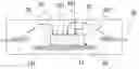
Referring to FIG. 3, the chip package of the present invention comprises a base 10 and a conductive layer 101 is coated on the base 10 by using adherent agent 30. A chip 20 is fixed to the base 10, wherein the conductive layer 101 is made by conductive metallic material which is gold, copper or aluminum.
The conductive layer 101 is located on the base 10 and a connection block 40 is connected to the conductive layer 101 on the base 10 by of ultrasonic oscillation in clean rooms so as to prevent impurities from being introduced between the base 10 and the connection block 40. The connection for connecting the connection block 40 to the base 10 is made prior the connection between the chip 20 and the base 10. By this way, the adherent agent can also be avoided from being introduced between the base 10 and the connection block 40. The connection block 40 is made by conductive metallic material which is gold, copper or aluminum.
When the connection block 40 and the chip 20 are respectively connected to the base 10, the gold wire is connected to the soldering needle (not shown) and a gold ball 501 is soldered to the top 201 of the chip 20, and then extends the gold wire 50 and connect the gold wire 50 to the top 401 of the connection block 40 by soldering. Therefore, the chip 20 is electrically connected to the base 10. The gold wire 50 is then used again to connect the chip 20 to the support 60. After the chip 20 is completely connected to the base 10, the packaging process can be started.
Due to the volume and the height of the connection block 40, when the chip 20 is connected to the base 10 by using the adherent agent 30, even if some of the adherent agent 30 overflows, the adherent agent 30 does not reach the top 401 of the connection block 40 where the gold wire 50 is to be soldered. Therefore, the delamination during packaging can be avoided and the defect rate can be reduced.
As shown in FIG. 4 which shows another embodiment of the present invention and which improves the connection between the gold wire 50 and the top 401 of the connection block 40. A gold ball 50 is formed on the top 401 of the connection block 40 before the gold wire 50 is soldered. The gold wire 50 forms a gold ball 501 on the top of the 201 of the chip 20 and the gold wire 50 is extended and connected to the top 401 of the connection block 40 by directly connecting the gold wire 50 to the gold ball 402 on the top 401 of the connection block 40. By this way, the gold wire 50 is firmly connected to the connection block 40 so as to reduce the defect rate.
While we have shown and described the embodiment in accordance with the present invention, it should be clear to those skilled in the art that further embodiments may be made without departing from the scope of the present invention.
Claims
What is claimed is:1. A chip package comprising:
a base having a conductive layer coated thereon;
a chip connected to the base by adherent agent;
a connection block connected to the conductive layer on the base and being electrically connected with the base, and
a gold wire having two ends thereof respectively connected to the chip and the connection block.
2. The chip package as claimed in claim 1, wherein the conductive layer is made by conductive metallic material which is gold, copper or aluminum.
3. The chip package as claimed in claim 1, wherein the connection block is made by conductive metallic material which is gold, copper or aluminum.
4. The chip package as claimed in claim 1, wherein the connection block is connected to the base by way of ultrasonic oscillation in clean rooms.
5. The chip package as claimed in claim 1, wherein the connection lock has a gold ball on a top thereof so as to connect the gold wire with the connection block.
Images & Drawings included:

Sources:
- United States Patent and Trademark Office - verify current appl. status at the USPTO↗
Similar patent applications:
- » 20150069626
CHIP PACKAGE, CHIP PACKAGE MODULE BASED ON THE CHIP PACKAGE, AND METHOD OF MANUFACTURING THE CHIP PACKAGE - » 20170356968
Chip package, a chip package system, a method of manufacturing a chip package, and a method of operating a chip package - » 20110272716
Lead frame for chip package, chip package, package module, and illumination apparatus including chip package module - » 20060088955
Chip package, chip packaging, chip carrier and process thereof - » 20240413138
CHIP PACKAGING METHOD, CHIP PACKAGING MODULE, AND EMBEDDED SUBSTRATE CHIP PACKAGING STRUCTURE - » 20230064442
CHIP PACKAGE STRUCTURE, CHIP PACKAGE SYSTEM, AND METHOD OF FORMING A CHIP PACKAGE STRUCTURE - » 20240421137
CHIP PACKAGE UNIT, CHIP PACKAGE STACK MODULE, AND METHOD OF MANUFACTURING CHIP PACKAGE STACK MODULE - » 20140151701
Embedded chip package, a chip package, and a method for manufacturing an embedded chip package - » 20090321776
Multi-chip package for LED chip and multi-chip package LED device including the multi-chip package - » 20120087099
Printed Circuit Board For Board-On-Chip Package, Board-On-Chip Package Including The Same, And Method Of Fabricating The Board-On-Chip Package
Recent applications in this class:
- » 20250157893 2025-05-15
DISCRETE SEMICONDUCTOR DEVICE PACKAGE WITH LEAD FRAME CLIP - » 20250125228 2025-04-17
METHOD OF MANUFACTURING SEMICONDUCTOR DEVICES AND CORRESPONDING SEMICONDUCTOR DEVICE - » 20250112127 2025-04-03
IC ASSEMBLIES WITH METAL PASSIVATION AT BOND INTERFACES - » 20250105103 2025-03-27
SEMICONDUCTOR PACKAGE INCLUDING ONE OR MORE SOLDER JOINTS ELECTRICALLY AND MECHANICALLY COUPLING FIRST AND SECOND POWER SEMICONDUCTOR CHIPS TO A LEADFRAME PART AND METHOD FOR FABRICATING THEA SEMICONDUCTOR PACKAGE - » 20250096078 2025-03-20
SEMICONDUCTOR DEVICE AND METHOD OF MANUFACTURING THE SAME - » 20250029901 2025-01-23
COMPACT DIRECT-BONDED METAL SUBSTRATE PACKAGE - » 20250006597 2025-01-02
SEMICONDUCTOR DEVICE AS WELL AS A METHOD FOR MANUFACTURING SUCH SEMICONDUCTOR DEVICE - » 20240421044 2024-12-19
Die-Attach Fillet Height Reduction - » 20240421043 2024-12-19
SUBSTRATE PROCESS FLOW FOR ENABLING SUBSTRATE TO DIE HYBRID BONDING - » 20240404924 2024-12-05
SEMICONDUCTOR PACKAGE AND FABRICATION METHOD THEREOF
Recent applications for this Assignee:
- » 20130070427 2013-03-21
Pre molded can package - » 20130070424 2013-03-21
Molded can package - » 20110127658 2011-06-02
Muti Thickness Lead Frame