Method of manufacturing a semiconductor component
US20120282772A1
2012-11-08
13/460,939
2012-05-01
✅ Patent granted
US 8,802,564 B2
2014-08-12
-
-
Caridad Everhart
McCormick, Paulding & Huber LLP
2032-07-20
Abstract:
A method of manufacturing a semiconductor component includes the steps of manufacturing of a wafer, applying structures of components on the wafer to form a wafer assembly, applying a metal coating on the wafer, removing the metal coating in non-contact areas of the components, applying surrounds on the edge areas of the components, arranging the wafer on a foil held by a clamping ring, separating the components of the wafer compound carried by the foil from one another, arranging a covering mask on the areas of the separated components carried by the foil which are not to be coated, applying a metal coating on the separate components covered with the mask, removal of the mask, and removal of the components from the foil and further processing the separate components wherein that applying a metal coating on the separate components covered by the mask takes place by means of thermal spraying.
Assignee:
- Danfoss Silicon Power GmbH 14 🇩🇪 Schleswig, Germany
Applicant:
Interested in similar patents?
Get notified when new applications in this technology area are published.
Classification:
H01L21/568 » CPC main
Processes or apparatus adapted for the manufacture or treatment of semiconductor or solid state devices or of parts thereof; Manufacture or treatment of semiconductor devices or of parts thereof the devices having at least one potential-jump barrier or surface barrier, e.g. PN junction, depletion layer or carrier concentration layer; Assembly of semiconductor devices using processes or apparatus not provided for in a single one of the subgroups - , e.g. sealing of a cap to a base of a container; Encapsulations, e.g. encapsulation layers, coatings Temporary substrate used as encapsulation process aid
C23C4/01 » CPC further
Coating by spraying the coating material in the molten state, e.g. by flame, plasma or electric discharge Selective coating, e.g. pattern coating, without pre-treatment of the material to be coated
C23C4/02 » CPC further
Coating by spraying the coating material in the molten state, e.g. by flame, plasma or electric discharge Pretreatment of the material to be coated, e.g. for coating on selected surface areas
C23C4/134 » CPC further
Coating by spraying the coating material in the molten state, e.g. by flame, plasma or electric discharge characterised by the method of spraying Plasma spraying
C23C4/18 » CPC further
Coating by spraying the coating material in the molten state, e.g. by flame, plasma or electric discharge After-treatment
H01L21/561 » CPC further
Processes or apparatus adapted for the manufacture or treatment of semiconductor or solid state devices or of parts thereof; Manufacture or treatment of semiconductor devices or of parts thereof the devices having at least one potential-jump barrier or surface barrier, e.g. PN junction, depletion layer or carrier concentration layer; Assembly of semiconductor devices using processes or apparatus not provided for in a single one of the subgroups - , e.g. sealing of a cap to a base of a container; Encapsulations, e.g. encapsulation layers, coatings Batch processing
H01L21/6836 » CPC further
Processes or apparatus adapted for the manufacture or treatment of semiconductor or solid state devices or of parts thereof; Apparatus specially adapted for handling semiconductor or electric solid state devices during manufacture or treatment thereof; Apparatus specially adapted for handling wafers during manufacture or treatment of semiconductor or electric solid state devices or components ; Apparatus not specifically provided for elsewhere for supporting or gripping using temporarily an auxiliary support Wafer tapes, e.g. grinding or dicing support tapes
H01L24/03 » CPC further
Arrangements for connecting or disconnecting semiconductor or solid-state bodies; Methods or apparatus related thereto; Means for bonding being attached to, or being formed on, the surface to be connected, e.g. chip-to-package, die-attach, "first-level" interconnects; Manufacturing methods related thereto; Bonding areas ; Manufacturing methods related thereto Manufacturing methods
H01L24/05 » CPC further
Arrangements for connecting or disconnecting semiconductor or solid-state bodies; Methods or apparatus related thereto; Means for bonding being attached to, or being formed on, the surface to be connected, e.g. chip-to-package, die-attach, "first-level" interconnects; Manufacturing methods related thereto; Bonding areas ; Manufacturing methods related thereto; Structure, shape, material or disposition of the bonding areas prior to the connecting process of an individual bonding area
H01L24/93 » CPC further
Arrangements for connecting or disconnecting semiconductor or solid-state bodies; Methods or apparatus related thereto Batch processes
H01L2221/68327 » CPC further
Processes or apparatus adapted for the manufacture or treatment of semiconductor or solid state devices or of parts thereof covered by; Apparatus for handling semiconductor or electric solid state devices during manufacture or treatment thereof; Apparatus for handling wafers during manufacture or treatment of semiconductor or electric solid state devices or components; Apparatus not specifically provided for elsewhere for supporting or gripping using temporarily an auxiliary support used during dicing or grinding
H01L2224/03002 » CPC further
Indexing scheme for arrangements for connecting or disconnecting semiconductor or solid-state bodies and methods related thereto as covered by; Means for bonding being attached to, or being formed on, the surface to be connected, e.g. chip-to-package, die-attach, "first-level" interconnects; Manufacturing methods related thereto; Bonding areas; Manufacturing methods related thereto; Manufacturing methods; Involving a temporary auxiliary member not forming part of the manufacturing apparatus, e.g. removable or sacrificial coating, film or substrate for supporting the semiconductor or solid-state body
H01L2224/03418 » CPC further
Indexing scheme for arrangements for connecting or disconnecting semiconductor or solid-state bodies and methods related thereto as covered by; Means for bonding being attached to, or being formed on, the surface to be connected, e.g. chip-to-package, die-attach, "first-level" interconnects; Manufacturing methods related thereto; Bonding areas; Manufacturing methods related thereto; Manufacturing methods by blanket deposition of the material of the bonding area in liquid form Spray coating
H01L2224/03442 » CPC further
Indexing scheme for arrangements for connecting or disconnecting semiconductor or solid-state bodies and methods related thereto as covered by; Means for bonding being attached to, or being formed on, the surface to be connected, e.g. chip-to-package, die-attach, "first-level" interconnects; Manufacturing methods related thereto; Bonding areas; Manufacturing methods related thereto; Manufacturing methods by blanket deposition of the material of the bonding area in solid form using a powder
H01L2224/03444 » CPC further
Indexing scheme for arrangements for connecting or disconnecting semiconductor or solid-state bodies and methods related thereto as covered by; Means for bonding being attached to, or being formed on, the surface to be connected, e.g. chip-to-package, die-attach, "first-level" interconnects; Manufacturing methods related thereto; Bonding areas; Manufacturing methods related thereto; Manufacturing methods by blanket deposition of the material of the bonding area in gaseous form
H01L2224/94 » CPC further
Indexing scheme for arrangements for connecting or disconnecting semiconductor or solid-state bodies and methods related thereto as covered by; Batch processes at wafer-level, i.e. with connecting carried out on a wafer comprising a plurality of undiced individual devices
H01L2924/01005 » CPC further
Indexing scheme for arrangements or methods for connecting or disconnecting semiconductor or solid-state bodies as covered by; Chemical elements Boron [B]
H01L2924/01006 » CPC further
Indexing scheme for arrangements or methods for connecting or disconnecting semiconductor or solid-state bodies as covered by; Chemical elements Carbon [C]
H01L2924/00014 » CPC further
Indexing scheme for arrangements or methods for connecting or disconnecting semiconductor or solid-state bodies as covered by; Technical content checked by a classifier the subject-matter covered by the group, the symbol of which is combined with the symbol of this group, being disclosed without further technical details
H01L2224/93 » CPC further
Indexing scheme for arrangements for connecting or disconnecting semiconductor or solid-state bodies and methods related thereto as covered by Batch processes
H01L2224/03 » CPC further
Indexing scheme for arrangements for connecting or disconnecting semiconductor or solid-state bodies and methods related thereto as covered by; Means for bonding being attached to, or being formed on, the surface to be connected, e.g. chip-to-package, die-attach, "first-level" interconnects; Manufacturing methods related thereto; Bonding areas; Manufacturing methods related thereto Manufacturing methods
H01L21/283 IPC
Processes or apparatus adapted for the manufacture or treatment of semiconductor or solid state devices or of parts thereof; Manufacture or treatment of semiconductor devices or of parts thereof the devices having at least one potential-jump barrier or surface barrier, e.g. PN junction, depletion layer or carrier concentration layer the devices having semiconductor bodies comprising elements of Group IV of the Periodic System or AB compounds with or without impurities, e.g. doping materials; Manufacture of electrodes on semiconductor bodies using processes or apparatus not provided for in groups - Deposition of conductive or insulating materials for electrodes conducting electric current
H01L21/44 IPC
Processes or apparatus adapted for the manufacture or treatment of semiconductor or solid state devices or of parts thereof; Manufacture or treatment of semiconductor devices or of parts thereof the devices having at least one potential-jump barrier or surface barrier, e.g. PN junction, depletion layer or carrier concentration layer the devices having semiconductor bodies not provided for in groups, , , and with or without impurities, e.g. doping materials Manufacture of electrodes on semiconductor bodies using processes or apparatus not provided for in groups -
Description
CROSS REFERENCE TO RELATED APPLICATION
Applicants hereby claim foreign priority benefits under U.S.C. §119 from German Patent Application No. 10 2011 100 255.7 filed on May 3, 2011, the contents of which are incorporated by reference herein.
TECHNICAL FIELD
The invention concerns a method of manufacturing a semiconductor component.
BACKGROUND OF THE INVENTION
Such a method is described in U.S. Pat. No. 6,603,191 B2, featuring the application of a metal coating by means of galvanic deposit. When applying the contact layer on the wafer carrying the component, however, it is practically impossible to prevent the wafer from warping due to the galvanic deposit of a metal layer.
SUMMARY OF THE INVENTION
Thus, the invention is based on the task of preventing a warping when applying the contact layer.
According to the invention, this task is solved by means of the features of claim 1 and the single sub-claim defines a preferred embodiment of the invention.
A method of manufacturing a semiconductor component includes the following steps: manufacturing of a wafer, applying structures of components on the wafer to form a wafer assembly, applying a metal coating on the wafer, removing the metal coating in non-contact areas of the components, applying surrounds on the edge areas of the components, arranging the wafer on a foil held by a clamping ring, separating the components of the wafer compound carried by the foil from one another, arranging a covering mask on the areas of the separated components carried by the foil which are not to be coated, applying a metal coating on the separate components covered with the mask, removal of the mask, and removal of the components from the foil and further processing the separate components, wherein applying a metal coating on the separate components covered by the mask takes place by means of thermal spraying. The method of manufacturing a semiconductor component is such that the thermal spraying occurres by means of nano-powder plasma depositing.
BRIEF DESCRIPTION OF THE DRAWING
Further features and advantages of the invention occur from the following description, in which the invention is explained with reference to a drawing:
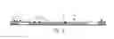
The single FIGURE shows a wafer arranged on a foil.
DETAILED DESCRIPTION OF THE PREFERRED EMBODIMENTS
The single FIGURE shows the wafer arranged on a foil, the components already being sawn and a metal coating being applied to the contact areas by means of thermal spraying, preferably nano-powder depositing.
Thus, in a manner known per se, the invention suggests manufacturing the wafer by creating the structures of the components and applying passivating surrounds on their edge areas. Subsequently, the wafer is placed on a foil held by a clamping ring, and the components carried by the foil are separated from one another, for example by sawing through the wafer assembly, whilst maintaining the integrity of the foil.
Then, a mask covering the areas of the components that are not to be coated is arranged on the individual components carried by the foil, and a metal coating is applied on the mask by spraying, or, preferably, by means of nano-powder plasma depositing. The mask is then removed and the components are removed from the foil and further processed.
The single FIGURE shows a wafer 2 that is formed by a plurality of components 1 formed by means of, for example, sawing. A mask 3 covers the areas of the separated components 1 which are carried by a foil 4. The FIGURE further shows a metal coating 5 applied on the mask 3 and the contact areas of the components by thermal spraying, or, preferably, by means of nano-powder plasma depositing.
With the suggested method featuring application of the metal coating by means of thermal spraying, a warping of the wafer is prevented.
While the present invention has been illustrated and described with respect to a particular embodiment thereof, it should be appreciated by those of ordinary skill in the art that various modifications to this invention may be made without departing from the spirit and scope of the present.
Claims
What is claimed is:1. A method of manufacturing a semiconductor component by means of the following steps:
manufacturing of a wafer,
applying structures of components on the wafer to form a wafer assembly,
applying a metal coating on the wafer,
removing the metal coating in non-contact areas of the components,
applying surrounds on the edge areas of the components,
arranging the wafer on a foil held by a clamping ring,
separating the components of the wafer compound carried by the foil from one another,
arranging a covering mask on the areas of the separated components carried by the foil which are not to be coated,
applying a metal coating on the separate components covered with the mask,
removal of the mask, and
removal of the components from the foil and further processing the separate components
wherein applying a metal coating on the separate components covered by the mask takes place by means of thermal spraying.
2. The method of manufacturing a semiconductor component according to claim 1, the thermal spraying occurring by means of nano-powder plasma depositing.
Images & Drawings included:

Sources:
- United States Patent and Trademark Office - verify current appl. status at the USPTO↗
Similar patent applications:
- » 20240282581
POLISHING LIQUID, POLISHING METHOD, COMPONENT MANUFACTURING METHOD, AND SEMICONDUCTOR COMPONENT MANUFACTURING METHOD - » 20250263582
POLISHING LIQUID, POLISHING METHOD, COMPONENT MANUFACTURING METHOD, AND SEMICONDUCTOR COMPONENT MANUFACTURING METHOD - » 20250263593
ABRASIVE GRAINS AND METHOD FOR SELECTING SAME, POLISHING LIQUID, MULTI-LIQUID TYPE POLISHING LIQUID, POLISHING METHOD, COMPONENT MANUFACTURING METHOD, AND SEMICONDUCTOR COMPONENT MANUFACTURING METHOD - » 20250187137
POLISHING SOLUTION, POLISHING METHOD, COMPONENT MANUFACTURING METHOD, AND SEMICONDUCTOR COMPONENT MANUFACTURING METHOD - » 20250257253
ABRASIVE GRAIN, SELECTION METHOD THEREFOR, POLISHING AGENT, MULTI-LIQUID POLISHING AGENT, POLISHING METHOD, COMPONENT MANUFACTURING METHOD, AND SEMICONDUCTOR COMPONENT MANUFACTURING METHOD - » 20240392162
POLISHING LIQUID, POLISHING METHOD, COMPONENT MANUFACTURING METHOD, AND SEMICONDUCTOR COMPONENT MANUFACTURING METHOD - » 20120153461
SEMICONDUCTOR COMPONENT, SEMICONDUCTOR WAFER COMPONENT, MANUFACTURING METHOD OF SEMICONDUCTOR COMPONENT, AND MANUFACTURING METHOD OF JOINING STRUCTURE - » 20180233473
Paste thermosetting resin composition, semiconductor component, semiconductor mounted article, method for manufacturing semiconductor component, and method for manufacturing semiconductor mounted article - » 20250178234
METHOD OF ADDITIVELY MANUFACTURING HIGH-PURITY SILICON, METHOD OF ADDITIVELY MANUFACTURING SEMICONDUCTOR MANUFACTURING EQUIPMENT COMPONENT, SEMICONDUCTOR MANUFACTURING EQUIPMENT COMPONENT, AND METHOD OF FORMING SEMICONDUCTOR MANUFACTURING EQUIPMENT COMPONENT - » 20080224298
Apparatus for packaging semiconductor devices, packaged semiconductor components, methods of manufacturing apparatus for packaging semiconductor devices, and methods of manufacturing semiconductor components
Recent applications in this class:
- » 20250293052 2025-09-18
LASER DE-BONDING CARRIERS AND COMPOSITE CARRIERS THEREOF - » 20250218801 2025-07-03
METHOD FOR MANUFACTURING ELECTRONIC COMPONENT OR SEMICONDUCTOR DEVICE - » 20250157830 2025-05-15
METHOD FOR MANUFACTURING INTEGRATED DEVICE PACKAGES - » 20250069903 2025-02-27
SEMICONDUCTOR DEVICE WITH EMBEDDED LEADFRAME AND METHOD THEREFOR - » 20250046626 2025-02-06
SEMICONDUCTOR DEVICE MANUFACTURING METHOD - » 20240412982 2024-12-12
SEMICONDUCTOR STRUCTURE AND MANUFACTURING METHOD THEREOF - » 20240395568 2024-11-28
METHOD FOR MANUFACTURING SEMICONDUCTOR DEVICE, TEMPORARY-FIXING MATERIAL, AND APPLICATION FOR MANUFACTURING SEMICONDUCTOR DEVICE OF TEMPORARY-FIXING MATERIAL - » 20240153786 2024-05-09
LASER DE-BONDING CARRIERS AND COMPOSITE CARRIERS THEREOF - » 20240145258 2024-05-02
PANEL LEVEL SEMICONDUCTOR PACKAGE AND METHOD OF MANUFACTURING THE SAME - » 20240087914 2024-03-14
METHOD OF MANUFACTURING AN ELECTRONIC DEVICE AND ELECTRONIC DEVICE MANUFACTURED THEREBY
Recent applications for this Assignee:
- » 20130228890 2013-09-05
Power semiconductor module with method for manufacturing a sintered power semiconductor module - » 20130032230 2013-02-07
FLOW DISTRIBUTOR - » 20120037688 2012-02-16
Method for producing a high-temperature and temperature-change resistant connection between a semiconductor module and a connection partner - » 20110255246 2011-10-20
Rigid power module suited for high-voltage applications - » 20110044001 2011-02-24
Cooling device for a plurality of power modules - » 20110017808 2011-01-27
Method for the low-temperature pressure sintering of electronic units to heat sinks - » 20100277873 2010-11-04
Method for manufacturing a rigid power module suited for high-voltage applications - » 20090146293 2009-06-11
Flow distribution module and a stack of flow distribution modules - » 20070215332 2007-09-20
Fluid cooling system - » 20070210445 2007-09-13
Power semiconductor module and method for cooling a power semiconductor module