Blank including a composite panel with semiconductor chips and plastic package molding compound and method and mold for producing the same
US20120286434A1
2012-11-15
13/556,837
2012-07-24
✅ Patent granted
US 8,524,542 B2
2013-09-03
-
-
Kimberly Rizkallah | Duy T Nguyen
2032-07-24
Abstract:
A blank and a semiconductor device include a composite panel with semiconductor chips embedded in a plastic package molding compound. The blank includes a composite panel with semiconductor chips arranged in rows and columns in a plastic package molding compound with active upper sides of the semiconductor chips forming a coplanar surface area with the upper side of the composite panel. The blank further includes an orientation indicator impressed into the plastic package molding compound when the semiconductor chips are embedded within the molding compound.
Inventors:
- Edward Fuergut 164 🇩🇪 Dasing, Germany
- Markus Brunnbauer 63 🇩🇪 Lappersdorf, Germany
- Markus Brunnbauer 1 🇩🇪 Lappersdof, Germany
Assignee:
- Intel Mobile Communications GmbH 563 🇩🇪 Neubiberg, Germany
- INTEL COMMUNICATIONS GMBH 1 🇩🇪 Neubiberg, Germany
Applicant:
Interested in similar patents?
Get notified when new applications in this technology area are published.
Classification:
H01L23/5389 » CPC main
Details of semiconductor or other solid state devices; Arrangements for conducting electric current within the device in operation from one component to another, i.e. interconnections, e.g. wires, lead frames the interconnection structure between a plurality of semiconductor chips being formed on, or in, insulating substrates the chips being integrally enclosed by the interconnect and support structures
H01L21/561 » CPC further
Processes or apparatus adapted for the manufacture or treatment of semiconductor or solid state devices or of parts thereof; Manufacture or treatment of semiconductor devices or of parts thereof the devices having at least one potential-jump barrier or surface barrier, e.g. PN junction, depletion layer or carrier concentration layer; Assembly of semiconductor devices using processes or apparatus not provided for in a single one of the subgroups - , e.g. sealing of a cap to a base of a container; Encapsulations, e.g. encapsulation layers, coatings Batch processing
H01L21/566 » CPC further
Processes or apparatus adapted for the manufacture or treatment of semiconductor or solid state devices or of parts thereof; Manufacture or treatment of semiconductor devices or of parts thereof the devices having at least one potential-jump barrier or surface barrier, e.g. PN junction, depletion layer or carrier concentration layer; Assembly of semiconductor devices using processes or apparatus not provided for in a single one of the subgroups - , e.g. sealing of a cap to a base of a container; Encapsulations, e.g. encapsulation layers, coatings; Moulds Release layers for moulds, e.g. release layers, layers against residue during moulding
H01L21/568 » CPC further
Processes or apparatus adapted for the manufacture or treatment of semiconductor or solid state devices or of parts thereof; Manufacture or treatment of semiconductor devices or of parts thereof the devices having at least one potential-jump barrier or surface barrier, e.g. PN junction, depletion layer or carrier concentration layer; Assembly of semiconductor devices using processes or apparatus not provided for in a single one of the subgroups - , e.g. sealing of a cap to a base of a container; Encapsulations, e.g. encapsulation layers, coatings Temporary substrate used as encapsulation process aid
H01L23/3107 » CPC further
Details of semiconductor or other solid state devices; Encapsulations, e.g. encapsulating layers, coatings, e.g. for protection characterised by the arrangement or shape the device being completely enclosed
H01L23/544 » CPC further
Details of semiconductor or other solid state devices Marks applied to semiconductor devices , e.g. registration marks,
H01L24/96 » CPC further
Arrangements for connecting or disconnecting semiconductor or solid-state bodies; Methods or apparatus related thereto; Batch processes at chip-level, i.e. with connecting carried out on a plurality of singulated devices, i.e. on diced chips the devices being encapsulated in a common layer, e.g. neo-wafer or pseudo-wafer, said common layer being separable into individual assemblies after connecting
H01L2223/54426 » CPC further
Details relating to semiconductor or other solid state devices covered by the group; Marks applied to semiconductor devices or parts for alignment
H01L2223/54473 » CPC further
Details relating to semiconductor or other solid state devices covered by the group; Marks applied to semiconductor devices or parts for use after dicing
H01L2223/54493 » CPC further
Details relating to semiconductor or other solid state devices covered by the group; Marks applied to semiconductor devices or parts Peripheral marks on wafers, e.g. orientation flats, notches, lot number
H01L2924/01006 » CPC further
Indexing scheme for arrangements or methods for connecting or disconnecting semiconductor or solid-state bodies as covered by; Chemical elements Carbon [C]
H01L2924/01027 » CPC further
Indexing scheme for arrangements or methods for connecting or disconnecting semiconductor or solid-state bodies as covered by; Chemical elements Cobalt [Co]
H01L2924/01033 » CPC further
Indexing scheme for arrangements or methods for connecting or disconnecting semiconductor or solid-state bodies as covered by; Chemical elements Arsenic [As]
H01L2924/01068 » CPC further
Indexing scheme for arrangements or methods for connecting or disconnecting semiconductor or solid-state bodies as covered by; Chemical elements Erbium [Er]
H01L2924/014 » CPC further
Indexing scheme for arrangements or methods for connecting or disconnecting semiconductor or solid-state bodies as covered by; Alloys Solder alloys
H01L2924/14 » CPC further
Indexing scheme for arrangements or methods for connecting or disconnecting semiconductor or solid-state bodies as covered by; Details of semiconductor or other solid state devices to be connected; Device type Integrated circuits
H01L2924/1815 » CPC further
Indexing scheme for arrangements or methods for connecting or disconnecting semiconductor or solid-state bodies as covered by; Details of package parts other than the semiconductor or other solid state devices to be connected; Encapsulation Shape
H01L2224/92 » CPC further
Indexing scheme for arrangements for connecting or disconnecting semiconductor or solid-state bodies and methods related thereto as covered by; Methods for connecting semiconductor or solid state bodies including different methods provided for in two or more of groups - Specific sequence of method steps
H01L2224/96 » CPC further
Indexing scheme for arrangements for connecting or disconnecting semiconductor or solid-state bodies and methods related thereto as covered by; Batch processes at chip-level, i.e. with connecting carried out on a plurality of singulated devices, i.e. on diced chips the devices being encapsulated in a common layer, e.g. neo-wafer or pseudo-wafer, said common layer being separable into individual assemblies after connecting
H01L2224/82 » CPC further
Indexing scheme for arrangements for connecting or disconnecting semiconductor or solid-state bodies and methods related thereto as covered by; Methods for connecting semiconductor or other solid state bodies using means for bonding being attached to, or being formed on, the surface to be connected by forming build-up interconnects at chip-level, e.g. for high density interconnects [HDI]
H01L2924/181 » CPC further
Indexing scheme for arrangements or methods for connecting or disconnecting semiconductor or solid-state bodies as covered by; Details of package parts other than the semiconductor or other solid state devices to be connected Encapsulation
H01L2924/12042 » CPC further
Indexing scheme for arrangements or methods for connecting or disconnecting semiconductor or solid-state bodies as covered by; Details of semiconductor or other solid state devices to be connected; Device type; Passive devices, e.g. 2 terminal devices; Optical Diode LASER
H01L2924/3511 » CPC further
Indexing scheme for arrangements or methods for connecting or disconnecting semiconductor or solid-state bodies as covered by; Technical effects; Mechanical effects; Thermal stress Warping
H01L2924/00 » CPC further
Indexing scheme for arrangements or methods for connecting or disconnecting semiconductor or solid-state bodies as covered by
H01L23/28 IPC
Details of semiconductor or other solid state devices Encapsulations, e.g. encapsulating layers, coatings, e.g. for protection
B28B23/00 IPC
Arrangements specially adapted for the production of shaped articles with elements wholly or partly embedded in the moulding material; Production of reinforced objects
H01L21/56 IPC
Processes or apparatus adapted for the manufacture or treatment of semiconductor or solid state devices or of parts thereof; Manufacture or treatment of semiconductor devices or of parts thereof the devices having at least one potential-jump barrier or surface barrier, e.g. PN junction, depletion layer or carrier concentration layer; Assembly of semiconductor devices using processes or apparatus not provided for in a single one of the subgroups - , e.g. sealing of a cap to a base of a container Encapsulations, e.g. encapsulation layers, coatings
H01L21/00 IPC
Processes or apparatus adapted for the manufacture or treatment of semiconductor or solid state devices or of parts thereof
Description
CROSS REFERENCE TO RELATED APPLICATIONS
This application is a continuation of U.S. patent application Ser. No. 11/686,368, filed on Mar. 15, 2007 and entitled “A Blank Comprising a Composite Panel with Semiconductor Chips and Plastic Package Molding Compound and Method and Mold for Producing the Same,” which claims priority under 35 U.S.C. §119 to Application No. DE 102006012738.2 filed on Mar. 17, 2006, entitled “Blank Comprising a Composite Panel with Semiconductor Chips and Plastic Package Molding Compound and Method and Mold for Producing the Same,” the entire contents of each application being hereby incorporated by reference.
BACKGROUND
So-called “embedded-die” technologies, where one or more semiconductor chips are surrounded with a plastic package by techniques such as molding-in, laminating-in or building-up of the plastic layer by layer, have numerous advantages over conventional technologies, where the semiconductor chip is applied to a substrate via contacts such as solder balls and is subsequently surrounded with a plastic package.
The “embedded-die” technologies therefore allow, for example, smaller and lighter devices and make the solid connection of a number of chips in a single package and a higher density of electrical connections possible.
Moreover, the “embedded-die” technologies offer advantages in production. A method is known for producing a semiconductor device with semiconductor chips molded into a plastic molding compound to form a composite panel or a blank, the active upper sides of the semiconductor chips forming a coplanar surface area with the upper side of the composite panel, while their edges and the rear side are covered by the plastic package molding compound. A wiring structure with interconnects that are separated from one another by dielectric layers can be applied particularly well and precisely to the coplanar surface area, without warping due to different materials with different coefficients of thermal expansion.
In the case of such a composite panel or a blank, it is imperative that, for example before the photolithographic processes, a determination of the orientation is carried out. For this purpose, laser markings are usually applied to the plastic packages. Applying these laser markings, however, requires a separate process step and consequently takes a considerable amount of time and incurs additional costs.
SUMMARY
A blank and a semiconductor device including a composite panel with semiconductor chips embedded in a plastic package molding compound are described herein and also a method and a mold for producing the same. The blank includes a composite panel with semiconductor chips arranged in rows and columns in a plastic package molding compound with active upper sides of the semiconductor chips forming a coplanar surface area with the upper side of the composite panel. The blank further includes an orientation indicator impressed into the plastic package molding compound when the semiconductor chips are embedded.
The above and still further features and advantages of the present invention will become apparent upon consideration of the following definitions, descriptions and descriptive figures of specific embodiments thereof, wherein like reference numerals in the various figures are utilized to designate like components. While these descriptions go into specific details of the invention, it should be understood that variations may and do exist and would be apparent to those skilled in the art based on the descriptions herein.
BRIEF DESCRIPTION OF THE DRAWINGS
Exemplary embodiments are explained in more detail below on the basis of the accompanying figures, where:
FIG. 1 shows a schematic cross section through a carrier with applied semiconductor chips;
FIG. 2 shows a schematic cross section through the carrier in a mold;
FIG. 3 shows a schematic cross section through the carrier in the mold at the end of the molding process;
FIG. 4 shows a schematic cross section through the carrier with semiconductor chips embedded into a plastic package molding compound;
FIG. 5 shows a schematic cross section through a self-supporting composite panel comprising the semiconductor chips embedded into the plastic package molding compound; and
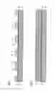
FIG. 6 shows a plan view of an exemplary composite panel with an impressed orientation indicator.
DETAILED DESCRIPTION
Described herein is a blank comprising a composite panel which allows a determination of the orientation, but can nevertheless be produced quickly and inexpensively. In addition, a mold for producing a blank with an orientation indicator and a method for producing semiconductor devices which is particularly simple and requires few process steps is described herein.
A blank comprises a composite panel with semiconductor chips arranged in semiconductor device positions in rows and columns, the semiconductor chips including an active upper side, a rear side and edge sides. The composite panel has an upper side which forms a coplanar surface area with the active upper sides of the semiconductor chips and the plastic package molding compound embedding at least the edge sides of the semiconductor chips. A wiring structure including interconnects and comprising one or more layers may be arranged on the upper side of the composite panel. For determining the orientation, the blank comprises an orientation indicator, which is impressed into the plastic package molding compound while the semiconductor chips are being embedded.
Any feature can be applied to the blank to serve as a suitable indicator that allows an indication regarding the orientation of the blank, by breaking the symmetry of the blank. Since, typically, no further requirements are expected of the orientation indicator, a separate process step just for applying the indicator represents an unjustifiably great effort. Instead, the molding step that is carried out in any case, that is to say the surrounding of the semiconductor devices with the plastic package molding compound, should be used for applying an orientation indicator.
During the molding, in particular the compression molding that is typically used when molding in the blank, the thermosetting or thermoplastic molding material, which may, for example, be in the form of a paste or a quantity of pellets and is generally preheated, is introduced into an open, usually heated mold cavity, which is subsequently closed. Via a pressing action, the molding material is forced into and completely filling the mold. The molding material remains in the mold until it has cured. This process can be used for applying an orientation indicator, by the mold being modified in such a way that it impresses an indicator on the blank.
As already mentioned, any feature that breaks up the symmetry of the blank is suitable as an orientation indicator. The choice of a suitable orientation indicator therefore also depends on the form of the blank. The blank may have the form of a semiconductor wafer. This is advantageous because it can then be worked in further processing steps with the infrastructure that is in any case present for the working of wafers.
In the case when a blank is in wafer form, it is appropriate to use orientation indicators that are also used for the identification of semiconductor wafers, for instance, notches at the edge of the wafer and for example what are known as flats. In an alternative embodiment, the blank is rectangular. In this case, notches or indicators in the form of beveled corners are likewise suitable as orientation indicators. However, other orientation indicators, for example in the central region of the blank, are conceivable for blanks in wafer form and for rectangular blanks.
A method for producing semiconductor devices comprises: first, producing a semiconductor wafer with a plurality or multiplicity of semiconductor chip positions arranged in rows and columns and separated into a plurality or multiplicity of semiconductor chips, which have active upper sides, edge sides and rear sides. These semiconductor chips are loaded onto a carrier with their active upper sides fixed on the carrier, in rows and columns.
Subsequently, in a molding process, a plastic package molding compound is applied to the carrier, embedding the semiconductor chips with their edge sides and their rear sides into the plastic package molding compound, thereby forming a composite panel with an upper side which forms a coplanar surface area with the upper sides of the semiconductor chips and thereby impressing an orientation indicator into the plastic package molding compound.
After the plastic package molding compound cures, the carrier is removed, thereby producing a self-supporting, largely warp-free blank. A wiring structure is applied to the then accessible upper side of the composite panel and the active upper sides of the semiconductor chips via photolithographic processes. In a final step, the blank is separated into individual semiconductor devices.
The described method has the advantage that it produces the described device without applying the orientation indicator in a separate step. The production of the semiconductor devices can consequently be accomplished with less time being expended and with lower costs being incurred.
A mold for embedding semiconductor devices into a plastic package molding compound, according to the described method, comprises walls which enclose a least one mold cavity. The mold cavity comprises one or more recesses and/or elevations with the effect that the orientation indicator is impressed into the plastic package molding compound of the blank during the molding. Elevations in the walls of the mold leave a notch behind in the compression-molded blank. The notch represents a clear orientation indicator but can be applied in the edge region of the blank, so that it does not cause any problems after the blank has been divided into individual semiconductor devices, but also allows the plastic package molding compound that is marked by the notch to be removed if need be. However, other, more complicated orientation indicators and/or orientation indicators applied in the central region of the blank are also conceivable.
In the following paragraphs, exemplary embodiments of the described device and method are described in connection with the figures.
Individual production stages of a blank 1 are represented in FIGS. 1 to 5 by schematic cross sections. A first method step, in which a semiconductor wafer is first produced and subsequently divided into individual semiconductor chips, is not represented. FIG. 1 shows only the result of the subsequent method step, in which the semiconductor chips 3, for example after a prior functional test, are placed onto a carrier 26 in semiconductor device positions 5. The carrier may have the form and the dimensions of a wafer, so that an artificial wafer is produced in the steps that follow, and the artificial wafer can be processed particularly easily by automatic equipment that is present in any case. It may, however, also have a different form, for example be rectangular. Metals, silicon or polymers are suitable for example as the material for the carrier.
The semiconductor chips 3 are not arranged closely adjacent one another but instead have interspaces 11 left between the individual semiconductor chips 3 and these are later filled with plastic package molding compound to form package walls of semiconductor devices.
The semiconductor chips 3 are fixed with their active upper sides 8 and the contact areas 19 located on the latter on the upper side 28 of the carrier 26 with the aid of a double-sided adhesive film 27. In order to apply the semiconductor chips 3 in the semiconductor device positions 5, an automatic placement machine (not represented) is used, picking up the parts of a semiconductor wafer that have been separated into semiconductor chips 3 and positioning and fixing them exactly on the upper side 28 of the carrier 26 with the aid of the film 27.
Subsequently, the semiconductor chips 3 are embedded in a plastic package molding compound 4 to form chip-scale packages, as shown in FIG. 2. For this purpose, the carrier 26 with the semiconductor chips 3 fixed on it is introduced into a mold cavity 21 of a mold 16, which has a lower part 18 for receiving the carrier 26 and another part 17 for closing the mold 16. The upper part 17 of the mold 16 may be covered on its inner side with a release layer 22, the lower part 18 of the mold 16 may be covered on its inner side with a further release layer 23. The release layer 22 and/or the further release layer 23 may be, for example, a coating of the mold 16 with a suitable material for a film placed into the mold 16.
The mold 16 comprises one or more elevations 29 or recesses (not represented) for applying an orientation indicator on the blank 1, the orientation indicator being impressed into the composite panel via an elevation 29, while raised orientation indicators are created by the likewise conceivable use of a recess. However, orientation indicators which are impressed in the composite panel, and even completely penetrate it, are particularly easily identifiable by optical methods.
The semiconductor chips 3 are embedded into a plastic package molding compound 4 via compression molding or transfer molding, a composite panel 2 comprising the plastic package molding compound 4 and the semiconductor chips 3 being formed, as shown in FIG. 3. While the composite panel 2 is located inside the mold cavity 21, it is delimited above by the release layer 22 and below by the adhesive film 27.
The elevation 29 impresses an orientation indicator into the composite panel 2, it being possible in this case for the orientation indicator to be a notch for example. The elevation 29 would then have only a small extent in the direction perpendicular to the plane of the drawing.
FIG. 4 shows a schematic cross section through the carrier 26 after applying a plastic package molding compound 4 into the interspaces 11 between the semiconductor chips 3 and to its rear sides 10. In this case, the active upper side 8 of the semiconductor chips 3 form a coplanar surface area 9 of the blank 1 with the plastic package molding compound 4.
After the plastic package molding compound 4 cures, a stable, self-supporting blank 1 with semiconductor chips 3 embedded in the plastic package molding compound 4 has been formed and the carrier 26 is removed together with the adhesive film 37. The removal of the carrier 26 may be performed by heating up the blank 1 and the carrier 26, the double-sided adhesive film 27 losing its adhesive effect and allowing the carrier 26 to be pulled off from the upper side 6 of the blank 1 without exerting any appreciable force on the blank 1. The result of this method step is shown in FIG. 5.
The active upper side 8 of the semiconductor chips 3 is then freely accessible, so that both the contact areas 19 and the remaining surface 8 of the semiconductor chips 3 and of the plastic package molding compound 4 are available for photolithographic processes. For this, it is particularly important that a determination of the orientation of the blank is possible.
Examples of conceivable orientation indicators that can easily be applied during the molding are represented in FIG. 6. FIG. 6 shows a schematic plan view of a composite panel of a blank 1. A multiplicity of semiconductor device positions 5 are arranged, with at least one semiconductor chip 3 in each case, in rows 24 and columns 25 in a plastic package molding compound 4 in such a way that the edge sides 12, 13, 14 and 15 and also the rear side 10 (not visible in FIG. 6) of the semiconductor chips 3 are in each case embedded by the plastic package molding compound 4, while the active upper side 8 (visible here) of the semiconductor chips 3 is freely accessible. The rear side 10 may be embedded in the plastic package molding compound 4, but does not have to be. The plastic package molding compound 4 and the active upper sides 8 of the semiconductor chips 3 form a coplanar upper side 6 of the composite panel. Arranged on the coplanar upper side 6 of the composite panel, in the region of the active upper side 8 of the semiconductor chips 3, are contact areas 19, which are electrically in connection with the individual semiconductor elements of an integrated circuit of the semiconductor chip 3.
In FIG. 6, the blank comprises, for example, two orientation indicators 30a and 30b, although typically only one orientation indicator is applied. Here, a notched edge or notch 30a and a truncated or beveled corner 30b are shown as examples. In the case of a blank in wafer form, a notch 30a would likewise be a suitable orientation indicator, and a flat would also be conceivable for example.
While the invention has been described in detail with reference to specific embodiments thereof, it will be apparent to one of ordinary skill in the art that various changes and modifications can be made therein without departing from the spirit and scope thereof. Accordingly, it is intended that the present invention covers the modifications and variations of this invention provided they come within the scope of the appended claims and their equivalents.
Claims
What is claimed is:1. A blank comprising
a composite panel including at least one orientation indicator disposed on the composite panel;
a plurality of semiconductor chips arranged in semiconductor device positions in rows and columns along the panel, wherein each of the semiconductor chips includes an active upper side, a rear side and edge sides, and the active upper sides of the semiconductor chips are substantially coplanar with an upper side of the composite panel;
wherein the composite panel is formed from a plastic package molding compound that embeds at least the edge and rear sides of the semiconductor chips and is impressed to form the composite panel with semiconductor chips embedded therein while forming the at least one orientation indicator.
2. The blank of claim 1, wherein the blank has substantially the form and dimensions of a semiconductor wafer.
3. The blank of claim 1, wherein the at least one orientation indicator comprises a beveled corner portion of the blank.
4. The blank of claim 1, wherein the blank is substantially rectangular.
5. The blank of claim 1, wherein the orientation indicator comprises a notch located at an edge portion of the blank.
6. A method for producing semiconductor devices, the method comprising:
producing a semiconductor wafer with a plurality of semiconductor chip positions;
separating the semiconductor wafer into a plurality of individual semiconductor chips, each semiconductor chip including an active upper side, edge sides and a rear side;
loading a carrier with semiconductor chips in semiconductor device positions arranged in rows and columns such that the active upper sides of the semiconductor chips are fixed to the carrier;
applying a plastic package molding compound via a molding process to the carrier such that an orientation indicator is impressed into the plastic package molding compound and the semiconductor chips including the rear and edge sides of the semiconductor chips are embedded into the plastic package molding compound;
removing the carrier from the plastic package molding compound to form a self-supporting blank comprising a composite panel, wherein the composite panel includes the orientation indicator, semiconductor chips embedded within the composite panel, and an upper side of the composite panel is substantially coplanar with exposed active upper sides of the semiconductor chips;
applying a wiring structure to the upper side of the composite panel and the active upper sides of the semiconductor chips; and
separating the blank into individual semiconductor devices.
7. The method of claim 6, wherein the composite panel is formed having substantially the form and dimensions of a semiconductor wafer.
8. The method of claim 6, wherein the orientation indicator comprises a beveled edge of the composite panel.
9. The method of claim 6, wherein the composite panel is formed having substantially a rectangular shape.
10. The method of claim 6, wherein the orientation indicator comprises a notch.
11. A mold for embedding semiconductor devices into a plastic package molding compound, the mold comprising at least one mold cavity including a recess or elevation configured to impress an orientation indicator into the plastic package molding compound.
Images & Drawings included:


Sources:
- United States Patent and Trademark Office - verify current appl. status at the USPTO↗
Similar patent applications:
Recent applications in this class:
- » 20250293174 2025-09-18
SEMICONDUCTOR DEVICE AND METHOD OF MANUFACTURE - » 20250293173 2025-09-18
CHIP PACKAGE AND METHOD OF FORMING THE SAME - » 20250293172 2025-09-18
SEMICONDUCTOR PACKAGE WITH BRIDGE DIE OVER EMBEDDED INTERPOSER - » 20250285986 2025-09-11
SCALABLE ELECTRONICS MANUFACTURING WITH RIGID TILE PANEL EMBEDDING - » 20250273586 2025-08-28
PACKAGE COMPRISING A BASE PORTION AND INTEGRATED DEVICES - » 20250273585 2025-08-28
PACKAGE COMPRISING SUBSTRATES AND INTEGRATED DEVICES - » 20250266367 2025-08-21
CHIP PACKAGE AND MANUFACTURING METHOD THEREOF - » 20250266366 2025-08-21
PACKAGING STRUCTURE, METHOD FOR PREPARING PACKAGING STRUCTURE, AND ELECTRONIC DEVICE - » 20250253261 2025-08-07
ELECTRONIC PACKAGE AND MANUFACTURING METHOD THEREOF - » 20250253260 2025-08-07
CHIP PACKAGE AND METHOD OF FORMING THE SAME
Recent applications for this Assignee:
- » 20180255533 2018-09-06
MULTIBAND-OPERATION IN WIRELESS COMMUNICATION SYSTEMS - » 20180013460 2018-01-11
Radio-frequency front-end and receiver - » 20150109939 2015-04-23
Minimization of drive tests uplink measurements - » 20150079913 2015-03-19
Semiconductor device and fabrication method - » 20150011207 2015-01-08
Method and related mobile device for searching for a mobile network - » 20150003573 2015-01-01
Method and device for channel estimation with colliding interference cancellation - » 20150003542 2015-01-01
Channel estimation technique - » 20150003509 2015-01-01
Interference cancellation radio receiver - » 20140359020 2014-12-04
Method and apparatus for requesting media replication in a collaborative communication session, and method and apparatus for assigning a communication medium for a collaborative communication session - » 20140344368 2014-11-20
Method and apparatus for requesting media replication in a collaborative communication session, and method and apparatus for assigning a communication medium for a collaborative communication session