Chip package and method for forming the same
US20130307161A1
2013-11-21
13/895,219
2013-05-15
✅ Patent granted
US 9,570,398 B2
2017-02-14
-
-
Eva Y Montalvo | Nga Doan
Liu & Liu
2034-03-23
Abstract:
An embodiment of the invention provides a chip package which includes: a first substrate; a second substrate disposed thereon, wherein the second substrate includes a lower semiconductor layer, an upper semiconductor layer, and an insulating layer therebetween, and a portion of the lower semiconductor layer electrically contacts with at least one pad on the first substrate; a conducting layer disposed on the upper semiconductor layer of the second substrate and electrically connected to the portion of the lower semiconductor layer electrically contacting with the at least one pad; an opening extending from the upper semiconductor layer towards the lower semiconductor layer and extending into the lower semiconductor layer; and a protection layer disposed on the upper semiconductor layer and the conducting layer, wherein the protection layer extends onto a portion of a sidewall of the opening, and does not cover the lower semiconductor layer in the opening.
Inventors:
- Tsang-Yu LIU 125 🇹🇼 Zhubei City, Taiwan
- Shu-Ming CHANG 64 🇹🇼 New Taipei City, Taiwan
- Yen-Shih HO 84 🇹🇼 Kaohsiung City, Taiwan
- Yu-Ting HUANG 5 🇹🇼 Tainan City, Taiwan
- YEN-SHIH HO 69 🇹🇼 Kaohsiung, Taiwan
- Tsang-Yu Liu 98 🇹🇼 Zhubei, Taiwan
- Shu-Ming Chang 53 🇹🇼 New Taipei, Taiwan
- Yu-Ting Huang 4 🇹🇼 Tainan, Taiwan
Assignee:
- Xintec Inc. 49 🇹🇼 Jhongli City, Taiwan
- Xintec Inc. 161 🇹🇼 Taoyuan, Taiwan
Applicant:
Interested in similar patents?
Get notified when new applications in this technology area are published.
Classification:
H01L23/5384 » CPC main
Details of semiconductor or other solid state devices; Arrangements for conducting electric current within the device in operation from one component to another, i.e. interconnections, e.g. wires, lead frames the interconnection structure between a plurality of semiconductor chips being formed on, or in, insulating substrates Conductive vias through the substrate with or without pins, e.g. buried coaxial conductors
H01L23/481 » CPC further
Details of semiconductor or other solid state devices; Arrangements for conducting electric current to or from the solid state body in operation, e.g. leads, terminal arrangements ; Selection of materials therefor Internal lead connections, e.g. via connections, feedthrough structures
H01L24/92 » CPC further
Arrangements for connecting or disconnecting semiconductor or solid-state bodies; Methods or apparatus related thereto; Methods for connecting semiconductor or solid state bodies including different methods provided for in two or more of groups - Specific sequence of method steps
B81B2207/095 » CPC further
Microstructural systems or auxiliary parts thereof; Packages; Arrangements for connecting external electrical signals to mechanical structures inside the package; Feed-through, via through the lid
H01L21/6835 » CPC further
Processes or apparatus adapted for the manufacture or treatment of semiconductor or solid state devices or of parts thereof; Apparatus specially adapted for handling semiconductor or electric solid state devices during manufacture or treatment thereof; Apparatus specially adapted for handling wafers during manufacture or treatment of semiconductor or electric solid state devices or components ; Apparatus not specifically provided for elsewhere for supporting or gripping using temporarily an auxiliary support
H01L24/02 » CPC further
Arrangements for connecting or disconnecting semiconductor or solid-state bodies; Methods or apparatus related thereto; Means for bonding being attached to, or being formed on, the surface to be connected, e.g. chip-to-package, die-attach, "first-level" interconnects; Manufacturing methods related thereto Bonding areas ; Manufacturing methods related thereto
H01L24/03 » CPC further
Arrangements for connecting or disconnecting semiconductor or solid-state bodies; Methods or apparatus related thereto; Means for bonding being attached to, or being formed on, the surface to be connected, e.g. chip-to-package, die-attach, "first-level" interconnects; Manufacturing methods related thereto; Bonding areas ; Manufacturing methods related thereto Manufacturing methods
H01L24/05 » CPC further
Arrangements for connecting or disconnecting semiconductor or solid-state bodies; Methods or apparatus related thereto; Means for bonding being attached to, or being formed on, the surface to be connected, e.g. chip-to-package, die-attach, "first-level" interconnects; Manufacturing methods related thereto; Bonding areas ; Manufacturing methods related thereto; Structure, shape, material or disposition of the bonding areas prior to the connecting process of an individual bonding area
H01L24/08 » CPC further
Arrangements for connecting or disconnecting semiconductor or solid-state bodies; Methods or apparatus related thereto; Means for bonding being attached to, or being formed on, the surface to be connected, e.g. chip-to-package, die-attach, "first-level" interconnects; Manufacturing methods related thereto; Bonding areas ; Manufacturing methods related thereto; Structure, shape, material or disposition of the bonding areas after the connecting process of an individual bonding area
H01L24/11 » CPC further
Arrangements for connecting or disconnecting semiconductor or solid-state bodies; Methods or apparatus related thereto; Means for bonding being attached to, or being formed on, the surface to be connected, e.g. chip-to-package, die-attach, "first-level" interconnects; Manufacturing methods related thereto; Bump connectors ; Manufacturing methods related thereto Manufacturing methods
H01L24/13 » CPC further
Arrangements for connecting or disconnecting semiconductor or solid-state bodies; Methods or apparatus related thereto; Means for bonding being attached to, or being formed on, the surface to be connected, e.g. chip-to-package, die-attach, "first-level" interconnects; Manufacturing methods related thereto; Bump connectors ; Manufacturing methods related thereto; Structure, shape, material or disposition of the bump connectors prior to the connecting process of an individual bump connector
H01L24/29 » CPC further
Arrangements for connecting or disconnecting semiconductor or solid-state bodies; Methods or apparatus related thereto; Means for bonding being attached to, or being formed on, the surface to be connected, e.g. chip-to-package, die-attach, "first-level" interconnects; Manufacturing methods related thereto; Layer connectors, e.g. plate connectors, solder or adhesive layers; Manufacturing methods related thereto; Structure, shape, material or disposition of the layer connectors prior to the connecting process of an individual layer connector
H01L24/32 » CPC further
Arrangements for connecting or disconnecting semiconductor or solid-state bodies; Methods or apparatus related thereto; Means for bonding being attached to, or being formed on, the surface to be connected, e.g. chip-to-package, die-attach, "first-level" interconnects; Manufacturing methods related thereto; Layer connectors, e.g. plate connectors, solder or adhesive layers; Manufacturing methods related thereto; Structure, shape, material or disposition of the layer connectors after the connecting process of an individual layer connector
H01L24/80 » CPC further
Arrangements for connecting or disconnecting semiconductor or solid-state bodies; Methods or apparatus related thereto Methods for connecting semiconductor or other solid state bodies using means for bonding being attached to, or being formed on, the surface to be connected
H01L24/94 » CPC further
Arrangements for connecting or disconnecting semiconductor or solid-state bodies; Methods or apparatus related thereto; Batch processes at wafer-level, i.e. with connecting carried out on a wafer comprising a plurality of undiced individual devices
H01L2221/68381 » CPC further
Processes or apparatus adapted for the manufacture or treatment of semiconductor or solid state devices or of parts thereof covered by; Apparatus for handling semiconductor or electric solid state devices during manufacture or treatment thereof; Apparatus for handling wafers during manufacture or treatment of semiconductor or electric solid state devices or components; Apparatus not specifically provided for elsewhere for supporting or gripping using temporarily an auxiliary support Details of chemical or physical process used for separating the auxiliary support from a device or wafer
H01L2224/02331 » CPC further
Indexing scheme for arrangements for connecting or disconnecting semiconductor or solid-state bodies and methods related thereto as covered by; Means for bonding being attached to, or being formed on, the surface to be connected, e.g. chip-to-package, die-attach, "first-level" interconnects; Manufacturing methods related thereto; Bonding areas; Manufacturing methods related thereto; Redistribution layers [RDL] for bonding areas; Structure of the redistribution layers Multilayer structure
H01L2224/02371 » CPC further
Indexing scheme for arrangements for connecting or disconnecting semiconductor or solid-state bodies and methods related thereto as covered by; Means for bonding being attached to, or being formed on, the surface to be connected, e.g. chip-to-package, die-attach, "first-level" interconnects; Manufacturing methods related thereto; Bonding areas; Manufacturing methods related thereto; Redistribution layers [RDL] for bonding areas; Disposition of the redistribution layers connecting the bonding area on a surface of the semiconductor or solid-state body with another surface of the semiconductor or solid-state body
H01L2224/03002 » CPC further
Indexing scheme for arrangements for connecting or disconnecting semiconductor or solid-state bodies and methods related thereto as covered by; Means for bonding being attached to, or being formed on, the surface to be connected, e.g. chip-to-package, die-attach, "first-level" interconnects; Manufacturing methods related thereto; Bonding areas; Manufacturing methods related thereto; Manufacturing methods; Involving a temporary auxiliary member not forming part of the manufacturing apparatus, e.g. removable or sacrificial coating, film or substrate for supporting the semiconductor or solid-state body
H01L2224/0401 » CPC further
Indexing scheme for arrangements for connecting or disconnecting semiconductor or solid-state bodies and methods related thereto as covered by; Means for bonding being attached to, or being formed on, the surface to be connected, e.g. chip-to-package, die-attach, "first-level" interconnects; Manufacturing methods related thereto; Bonding areas; Manufacturing methods related thereto; Structure, shape, material or disposition of the bonding areas prior to the connecting process Bonding areas specifically adapted for bump connectors, e.g. under bump metallisation [UBM]
H01L2224/8385 » CPC further
Indexing scheme for arrangements for connecting or disconnecting semiconductor or solid-state bodies and methods related thereto as covered by; Methods for connecting semiconductor or other solid state bodies using means for bonding being attached to, or being formed on, the surface to be connected using a layer connector; Bonding techniques using a polymer adhesive, e.g. an adhesive based on silicone, epoxy, polyimide, polyester
H01L2224/92 » CPC further
Indexing scheme for arrangements for connecting or disconnecting semiconductor or solid-state bodies and methods related thereto as covered by; Methods for connecting semiconductor or solid state bodies including different methods provided for in two or more of groups - Specific sequence of method steps
H01L2224/94 » CPC further
Indexing scheme for arrangements for connecting or disconnecting semiconductor or solid-state bodies and methods related thereto as covered by; Batch processes at wafer-level, i.e. with connecting carried out on a wafer comprising a plurality of undiced individual devices
H01L2924/1306 » CPC further
Indexing scheme for arrangements or methods for connecting or disconnecting semiconductor or solid-state bodies as covered by; Details of semiconductor or other solid state devices to be connected; Device type; Discrete devices, e.g. 3 terminal devices; Transistor Field-effect transistor [FET]
H01L2924/13091 » CPC further
Indexing scheme for arrangements or methods for connecting or disconnecting semiconductor or solid-state bodies as covered by; Details of semiconductor or other solid state devices to be connected; Device type; Discrete devices, e.g. 3 terminal devices; Transistor; Field-effect transistor [FET] Metal-Oxide-Semiconductor Field-Effect Transistor [MOSFET]
H01L2924/1461 » CPC further
Indexing scheme for arrangements or methods for connecting or disconnecting semiconductor or solid-state bodies as covered by; Details of semiconductor or other solid state devices to be connected; Mixed devices MEMS
H01L23/538 IPC
Details of semiconductor or other solid state devices; Arrangements for conducting electric current within the device in operation from one component to another, i.e. interconnections, e.g. wires, lead frames the interconnection structure between a plurality of semiconductor chips being formed on, or in, insulating substrates
H01L23/48 IPC
Details of semiconductor or other solid state devices Arrangements for conducting electric current to or from the solid state body in operation, e.g. leads, terminal arrangements ; Selection of materials therefor
B81B7/00 IPC
Microstructural systems; Auxiliary parts of microstructural devices or systems
H01L21/683 IPC
Processes or apparatus adapted for the manufacture or treatment of semiconductor or solid state devices or of parts thereof; Apparatus specially adapted for handling semiconductor or electric solid state devices during manufacture or treatment thereof; Apparatus specially adapted for handling wafers during manufacture or treatment of semiconductor or electric solid state devices or components ; Apparatus not specifically provided for elsewhere for supporting or gripping
H01L23/60 » CPC further
Details of semiconductor or other solid state devices; Structural electrical arrangements for semiconductor devices not otherwise provided for, e.g. in combination with batteries Protection against electrostatic charges or discharges, e.g. Faraday shields
B81B7/007 » CPC further
Microstructural systems; Auxiliary parts of microstructural devices or systems; Packages or encapsulation Interconnections between the MEMS and external electrical signals
H01L24/83 » CPC further
Arrangements for connecting or disconnecting semiconductor or solid-state bodies; Methods or apparatus related thereto; Methods for connecting semiconductor or other solid state bodies using means for bonding being attached to, or being formed on, the surface to be connected using a layer connector
H01L21/78 » CPC further
Processes or apparatus adapted for the manufacture or treatment of semiconductor or solid state devices or of parts thereof; Manufacture or treatment of devices consisting of a plurality of solid state components formed in or on a common substrate or of parts thereof; Manufacture of integrated circuit devices or of parts thereof; Manufacture or treatment of devices consisting of a plurality of solid state components or integrated circuits formed in, or on, a common substrate with subsequent division of the substrate into plural individual devices
H01L23/00 IPC
Details of semiconductor or other solid state devices
B81B2207/096 » CPC further
Microstructural systems or auxiliary parts thereof; Packages; Arrangements for connecting external electrical signals to mechanical structures inside the package; Feed-through, via through the substrate
H01L2221/68327 » CPC further
Processes or apparatus adapted for the manufacture or treatment of semiconductor or solid state devices or of parts thereof covered by; Apparatus for handling semiconductor or electric solid state devices during manufacture or treatment thereof; Apparatus for handling wafers during manufacture or treatment of semiconductor or electric solid state devices or components; Apparatus not specifically provided for elsewhere for supporting or gripping using temporarily an auxiliary support used during dicing or grinding
H01L2924/10155 » CPC further
Indexing scheme for arrangements or methods for connecting or disconnecting semiconductor or solid-state bodies as covered by; Details of semiconductor or other solid state devices to be connected; Shape being other than a cuboid
Description
CROSS REFERENCE TO RELATED APPLICATIONS
This application claims the benefit of U.S. Provisional Application No. 61/649,185, filed on May 18, 2012, the entirety of which is incorporated by reference herein.
BACKGROUND OF THE INVENTION
1. Field of the Invention
The present invention relates to a chip package, and in particular, relates to a multi-chip package.
2. Description of the Related Art
Along with the trend towards lighter, thinner, shorter, and smaller electronic devices, current semiconductor chip package structures tend to be high performance, multi-functional multi-chip package (MCP) structures. Multi-chip package (MCP) structures integrate a variety of semiconductor chips, such as logic chips, analog chips, control chips, memory chips, or micro-electro mechanical system (MEMS) chips, in a single package.
Improved multi-chip package technology is required.
BRIEF SUMMARY OF THE INVENTION
An embodiment of the invention provides a chip package, which includes: a first substrate; a second substrate disposed on the first substrate, wherein the second substrate comprises a lower semiconductor layer, an upper semiconductor layer, and an insulating layer therebetween, and a portion of the lower semiconductor layer electrically contacts with at least one pad on the first substrate; a conducting layer disposed on the upper semiconductor layer of the second substrate and electrically connected to the portion of the lower semiconductor layer electrically contacting with the at least one pad; an opening extending from the upper semiconductor layer towards the lower semiconductor layer and extending into the lower semiconductor layer; and a protection layer disposed on the upper semiconductor layer and the conducting layer, wherein the protection layer extends onto a portion of a sidewall of the opening, and does not cover the lower semiconductor layer in the opening.
An embodiment of the invention provides a method for forming a chip package, which includes: providing a first substrate; providing a second substrate including a lower semiconductor layer, an upper semiconductor layer, and an insulating layer therebetween; bonding the second substrate onto the first substrate such that a portion of the lower semiconductor layer electrically contacts with at least one pad on the first substrate; removing a portion of the upper semiconductor layer and a portion of the insulating layer to form an opening exposing an upper surface of the lower semiconductor layer; forming a conducting layer on the upper semiconductor layer of the second substrate, wherein the conducting layer is electrically connected to the portion of the lower semiconductor layer electrically contacting with the at least one pad; forming a protection layer on the upper semiconductor layer and the conducting layer, wherein the protection layer extends onto a sidewall of the opening, and does not cover a portion of the upper surface of the lower semiconductor layer in the opening; and removing a portion of the lower semiconductor layer from the upper surface of the lower semiconductor layer in the opening by using the protection layer as a mask, and thus the opening extends into the lower semiconductor layer.
A detailed description is given in the following embodiments with reference to the accompanying drawings.
BRIEF DESCRIPTION OF THE DRAWINGS
The present invention can be more fully understood by reading the subsequent detailed description and examples with references made to the accompanying drawings, wherein:
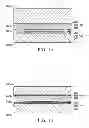
FIGS. 1A-1K are cross-sectional views of a manufacturing process of a chip package according to an embodiment of the present invention; and
FIG. 2 is a cross-sectional view of a chip package according to an embodiment of the present invention.
DETAILED DESCRIPTION OF THE INVENTION
The manufacturing method and method for use of the embodiment of the invention are illustrated in detail as followed. It should be appreciated, however, that the present invention provides many applicable inventive concepts that can be embodied in a wide variety of specific contexts. The specific embodiments discussed are merely illustrative of specific ways to make and use the invention, and do not limit the scope of the invention. In addition, the present disclosure may repeat reference numbers and/or letters in the various examples. This repetition is for the purpose of simplicity and clarity and does not in itself dictate a relationship between the various embodiments and/or configurations discussed. Furthermore, descriptions of a first material layer “on,” or “overlying” a second material layer, include embodiments where the first and second material layers are in direct contact and those where one or more material layers are interposing the first and second material layers.
A chip package according to an embodiment of the present invention may be used to package various chips. For example, the chip package of the embodiments of the invention may be applied to active or passive devices, or electronic components with digital or analog circuits, such as opto electronic devices, micro electro mechanical systems (MEMS), micro fluidic systems, and physical sensors for detecting heat, light, or pressure. Particularly, a wafer scale package (WSP) process may be applied to package semiconductor chips, such as image sensor devices, light-emitting diodes (LEDs), solar cells, RF circuits, accelerators, gyroscopes, micro actuators, surface acoustic wave devices, pressure sensors, ink printer heads, or power metal oxide semiconductor field effect transistor (MOSFET) modules.
The wafer scale package process mentioned above mainly means that after the package process is accomplished during the wafer stage, the wafer with chips is cut to obtain separate independent packages. However, in a specific embodiment, separate independent chips may be redistributed overlying a supporting wafer and then be packaged, which may also be referred to as a wafer scale package process. In addition, the above mentioned wafer scale package process may also be adapted to form chip packages of multi-layer integrated circuit devices by stacking a plurality of wafers having integrated circuits. In one embodiment, after the dicing process is performed, the obtained chip package is a chip scale package (CSP). The size of the chip scale package (CSP) may be only slightly larger than the size of the packaged chip. For example, the size of the chip scale package is not larger than 120% of the size of the packaged chip.
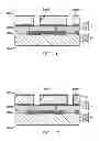
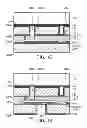
FIGS. 1A-1K are cross-sectional views of a manufacturing process of a chip package according to an embodiment of the present invention. As shown in FIG. 1A, substrates 10 and 20 are provided. In one embodiment, the substrates 10 and 20 are both semiconductor wafers, wherein the semiconductor wafers are, for example, but are not limited to a wafer with micro-electro mechanical systems (MEMS) and a wafer with complementary metal-oxide-semiconductor field effect transistors.
In one embodiment, the substrate 10 includes a lower semiconductor layer 104, an upper semiconductor layer 100 and an insulating layer 102 located between the lower semiconductor layer 104 and the upper semiconductor layer 100. The upper semiconductor layer 100 may have a surface 100a and a surface 100b, wherein the insulating layer 102 under the surface 100b may electrically insulate the upper semiconductor layer 100 from the lower semiconductor layer 104. In one embodiment, a plurality of gaps may be defined in the lower semiconductor layer 104, wherein the gaps divide the lower semiconductor layer 104 into a plurality of portions separated from each other.
In one embodiment, the substrate 20, such as a semiconductor wafer, includes a semiconductor substrate 200, pads 204 disposed on a surface 200a of the semiconductor substrate 200 and a dielectric layer 202 disposed on the surface 200a. The pads 204 may include a signal pad or a grounding pad.
In one embodiment, the substrate 10 may be bonded onto the substrate 20 such that a portion of the lower semiconductor layer 104 is bonded to and electrically contacts with at least one of the pads 204. In one embodiment, the pads 204 contacting the portion of the lower semiconductor layer 104 may be, but are not limited to grounding pads. In one embodiment, the bonding between the lower semiconductor layer 104 and the pads 204 may be a semiconductor-metal bonding, such as, but not limited to, germanium-aluminum bonding.
Then, as shown in FIG. 1B, the upper semiconductor layer 100 may be optionally thinned. A suitable thinning process includes, for example, a mechanical polishing process, a chemical mechanical polishing process, an etching process or combinations thereof.
Then, a conducting layer may be formed on the surface 100a of the upper semiconductor layer 100, wherein the conducting layer is electrically connected to the portion of the lower semiconductor layer 104 and the pads 204, such as grounding pads. The conducting layer may be electrically connected to the pads 204 via through holes and/or sidewalls of the substrate. However, for the sake of simplicity, the conducting layer in the embodiments described below is electrically connected to the pads 204 (such as grounding pads) via through holes.
As shown in FIG. 1C, a portion of the upper semiconductor layer 100 and a portion of the insulating layer 102 are removed from the surface 100a of the upper semiconductor layer 100 to form a hole 106a extending toward the lower semiconductor layer 104. In one embodiment, the hole 106a may be aligned with the pad 204 (such as a grounding pad) and the portion of the lower semiconductor layer 104 connecting to the pad 204. In another embodiment, the hole 106a may be aligned with the pad 204, but the pad 204, aligned with the hole 106a, does not contact the lower semiconductor layer 104. In another embodiment, the hole 106a is not aligned with the pad 204.
In one embodiment, a portion of the upper semiconductor layer 100 and a portion of the insulating layer 102 are removed from the surface 100a of the upper semiconductor layer 100 to form an opening 106b extending toward the lower semiconductor layer 104. The opening 106b may expose an upper surface of the lower semiconductor layer 104. In one embodiment, the opening 106b and the hole 106a may be formed during the same patterning process. In one embodiment, the shape and the distribution of the opening 106b are different from that of the hole 106a.
Then, as shown in FIG. 1D, a conducting layer 108 may be formed on the surface 100a of the upper semiconductor layer 100. In one embodiment, the conducting layer 108 may extend into the hole 106a to electrically contact with the lower semiconductor layer 104 exposed by the hole 106a. The lower semiconductor layer 104 exposed by the hole 106a may be electrically connected to the pad 204 (such as a grounding pad) on the semiconductor substrate 200. Thus, the conducting layer 108 may be electrically connected to the pad 204 for grounding applications. In one embodiment, the conducting layer 108 may be patterned to not extend into the opening 106b. In one embodiment, a side edge of the conducting layer 108, which is the closest to the opening 106b, and the opening 106b are spaced a distance apart. In one embodiment, the conducting layer 108 may directly contact the upper semiconductor layer 100. In one embodiment, the hole 106a may be located on a predetermined scribing line (not shown).
Furthermore, in other embodiments, in addition to grounding applications, the conducting layer 108 may be used as an electromagnetic interference shielding (EMI shielding) layer, a thermal conducting layer or a reflective layer.
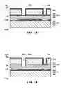
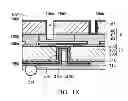
Then, as shown in FIG. 1E, a patterned protection layer 109 may be formed on the upper semiconductor layer 100 and the conducting layer 108. The protection layer 109 may include oxides, nitrides, nitrogen oxides or combinations thereof. In one embodiment, the protection layer 109 may be deposited by using chemical vapor depositions, coating techniques, spraying techniques, or other suitable processes. Then, the protection layer 109 may be patterned by using a photolithography process and an etching process. In one embodiment, the lower semiconductor layer 104 in the opening 106b is not covered by the protection layer 109 and thus is exposed. In one embodiment, the protection layer 109 may directly contact the conducting layer 108, the upper semiconductor layer 100 and the insulating layer 102.
Then, as shown in FIG. 1F, a portion of the lower semiconductor layer 104 is removed from the upper surface of the lower semiconductor layer 104 located in the opening 106b by using the protection layer 109 as a mask and thus the opening 106b extends into the lower semiconductor layer 104 to become an opening 106c. The protection layer 109 may extend onto a portion of the sidewall of the opening 106c, wherein the protection layer 109 may, for example, directly contact the upper semiconductor layer 100 and the insulating layer 102 on the sidewall of the opening 106c. The lower semiconductor layer 104 located in the opening 106c may not be covered by the protection layer 109. In one embodiment, the lower semiconductor layer 104 located at the bottom of the opening 106c may be used as, for example, a sensing region, such as, but not limited to, a pressure sensing region or a sound sensing region.
Then, as shown in FIG. 1G, a carrier substrate 110 may be optionally disposed on the upper semiconductor layer 100. For example, an adhesive layer 112 may be adopted to bond the carrier substrate 110 onto the protection layer 109 on the upper semiconductor layer 100. In one embodiment, the adhesive layer 112 may be a temporary adhesive layer, the adhesion of the adhesive layer 112 may be substantially eliminated after being exposed to light, heated or washed.
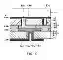
Then, as shown in FIG. 1H, the semiconductor substrate 200 may be optionally thinned. For example, the semiconductor substrate 200 may be thinned from the surface 200b of the semiconductor substrate 200 by using the carrier substrate 110 as a support.
As shown in FIG. 1H, a portion of the semiconductor substrate 200 may be removed from the surface 200b to form a hole 206 extending toward the pad 204, such as a signal pad.
Then, as shown in FIG. 1H, an insulating layer 208 may be formed on the surface 200b of the semiconductor substrate 200. The insulating layer 208 may extend onto the sidewall and the bottom of the hole 206. In one embodiment, the insulating layer 208 located on the bottom of the hole 206 may be removed by a patterning process to expose the pad 204 (e.g. a signal pad).
As shown in FIG. 1I, a conducting layer electrically connected to the pad 204 (e.g. a signal pad) is then formed on the insulating layer 208. For example, a seed layer 210a may be formed, and then a conducting layer 210b is formed by an electroplating process.
Then, as shown in FIG. 1J, a protection layer 212 may be formed on the conducting layer 210b and the insulating layer 208, and the protection layer 212 has at least one opening exposing a portion of the conducting layer 210b. Then, a signal conducting structure 214 may be formed in the opening, wherein the signal conducting structure 214 is, for example, a conductive bump or a solder ball.
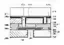
As shown in FIG. 1K, the adhesive layer 112 and the carrier substrate 110 thereon may be then removed. In one embodiment, the adhesive layer 112 and the carrier substrate 110 are removed by exposure to light, heating and/or using solvents. In the embodiment where the two substrates bonded to each other are two semiconductor wafers, a cutting process is performed along the predetermined scribing line (not shown) to cut the two substrates into a plurality of chip packages separated from each other. As shown in FIG. 1K, in one embodiment, the opening 106c may expose a thinner portion of the lower semiconductor layer 104 which may be used as, for example, a sensing region.
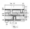
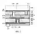
FIG. 2 is a cross-sectional view of a chip package according to an embodiment of the present invention, wherein same or similar reference numbers are used to designate same or similar elements. The embodiment of FIG. 2 is substantially the same as the embodiment of FIG. 1, except that the adhesive layer 112′ may be, but is not limited to, a permanent adhesive glue. Thus, in the embodiment of FIG. 2, the chip package still has the carrier substrate 110.
In the present embodiment, the signal conducting structure 214 of the chip package may be disposed on the lower surface of the chip package, and the (grounding) pads 204 may be electrically connected to the conducting layer 108 located on the chip package through the lower semiconductor layer 104. Thus, the distribution density of the conductive bumps on the lower surface of the chip package may be reduced. Furthermore, in the present embodiment, the opening may expose the lower semiconductor layer 104 for sensing applications, which may sense, for example, the change of pressure or sounds. The change of pressure or sounds sensed may be converted into electronic signals, and the electronic signals are then transmitted to the substrate 20 to be processed and are conducted out of the chip package for applications.
While the invention has been described by way of example and in terms of the preferred embodiments, it is to be understood that the invention is not limited to the disclosed embodiments. To the contrary, it is intended to cover various modifications and similar arrangements (as would be apparent to those skilled in the art). Therefore, the scope of the appended claims should be accorded the broadest interpretation so as to encompass all such modifications and similar arrangements.
Claims
What is claimed is:1. A chip package, comprising:
a first substrate;
a second substrate disposed on the first substrate, wherein the second substrate comprises a lower semiconductor layer, an upper semiconductor layer, and an insulating layer therebetween, and a portion of the lower semiconductor layer electrically contacts with at least one pad on the first substrate;
a conducting layer disposed on the upper semiconductor layer of the second substrate and electrically connected to the portion of the lower semiconductor layer electrically contacting with the at least one pad;
an opening extending from the upper semiconductor layer towards the lower semiconductor layer and extending into the lower semiconductor layer; and
a protection layer disposed on the upper semiconductor layer and the conducting layer, wherein the protection layer extends onto a portion of a sidewall of the opening, and does not cover the lower semiconductor layer in the opening.
2. The chip package as claimed in claim 1, further comprising:
a signal conducting structure disposed on a lower surface of the first substrate, wherein the signal conducting structure is electrically connected to a signal pad on the first substrate.
3. The chip package as claimed in claim 2, further comprising:
a second conducting layer electrically connected to the signal conducting structure and the signal pad.
4. The chip package as claimed in claim 3, further comprising:
a hole extending from a lower surface of the first substrate to the signal pad, wherein the second conducting layer extends into the hole to electrically contact with the signal pad, and a second insulating layer separates the second conducting layer from the first substrate.
5. The chip package as claimed in claim 1, wherein a side edge of the conducting layer, which is the closest to the opening, and the opening are spaced a distance apart.
6. The chip package as claimed in claim 1, further comprising:
a second hole extending from an upper surface of the upper semiconductor layer of the second substrate to the lower semiconductor layer of the second substrate, wherein the conducting layer extends into the second hole to electrically contact with the portion of the lower semiconductor layer.
7. The chip package as claimed in claim 6, wherein the second hole is aligned with one of the at least one pad.
8. The chip package as claimed in claim 1, wherein the conducting layer directly contacts with the second substrate.
9. The chip package as claimed in claim 1, wherein the protection layer directly contacts with the conducting layer, the upper semiconductor layer and the insulating layer.
10. The chip package as claimed in claim 1, further comprising:
a carrier substrate disposed on the second substrate.
11. A method for forming a chip package, comprising:
providing a first substrate;
providing a second substrate comprising a lower semiconductor layer, an upper semiconductor layer, and an insulating layer therebetween;
bonding the second substrate onto the first substrate such that a portion of the lower semiconductor layer electrically contacts with at least one pad on the first substrate;
removing a portion of the upper semiconductor layer and a portion of the insulating layer to form an opening exposing an upper surface of the lower semiconductor layer;
forming a conducting layer on the upper semiconductor layer of the second substrate, wherein the conducting layer is electrically connected to the portion of the lower semiconductor layer electrically contacting with the at least one pad;
forming a protection layer on the upper semiconductor layer and the conducting layer, wherein the protection layer extends onto a sidewall of the opening, and does not cover a portion of the upper surface of the lower semiconductor layer in the opening; and
removing a portion of the lower semiconductor layer from the upper surface of the lower semiconductor layer in the opening by using the protection layer as a mask, and thus the opening extends into the lower semiconductor layer.
12. The method for forming the chip package as claimed in claim 11, further comprising:
disposing a signal conducting structure on a lower surface of the first substrate, wherein the signal conducting structure is electrically connected to a signal pad on the first substrate.
13. The method for forming the chip package as claimed in claim 12, further comprising:
removing a portion of the first substrate from a lower surface of the first substrate to form a hole exposing the signal pad;
forming a second insulating layer on the lower surface of the first substrate and a sidewall of the second hole;
forming a second conducting layer on the lower surface of the first substrate, wherein the second conducting layer extends into the hole to electrically connect with the signal pad; and
forming the signal conducting structure on the second conducting layer on the lower surface of the first substrate.
14. The method for forming the chip package as claimed in claim 11, further comprising:
before forming the conducting layer, removing a portion of the upper semiconductor layer to form a second hole extending toward the lower semiconductor layer, and then forming the conducting layer extending into the second hole to electrically contact with the portion of the lower semiconductor layer.
15. The method for forming the chip package as claimed in claim 14, wherein the hole and the second opening are formed simultaneously.
16. The method for forming the chip package as claimed in claim 14, wherein the conducting layer substantially covers a sidewall and a bottom of the hole completely.
17. The method for forming the chip package as claimed in claim 11, further comprising:
bonding a carrier substrate onto the second substrate.
18. The method for forming the chip package as claimed in claim 17, further comprising:
removing the carrier substrate.
19. The method for forming the chip package as claimed in claim 11, wherein the protection layer directly contacts with the conducting layer, the upper semiconductor layer and the insulating layer.
20. The method for forming the chip package as claimed in claim 11, further comprising:
performing a cutting process on the first substrate and the second substrate to form a plurality of chip packages separated from each other.
Images & Drawings included:
Sources:
- United States Patent and Trademark Office - verify current appl. status at the USPTO↗
Similar patent applications:
- » 20210082861
Chip package, method of forming a chip package and method of forming an electrical contact - » 20220139798
Method of forming a chip package, method of forming a semiconductor arrangement, chip package, and semiconductor arrangement - » 20250079330
EMBEDDED CHIP-PACKAGE, SEMICONDUCTOR PACKAGE, METHOD OF FORMING AN EMBEDDED CHIP-PACKAGE, METHOD OF FORMING A SEMICONDUCTOR PACKAGE, AND METHOD OF ANALYZING AN EMBEDDED CHIP-PACKAGE OR A SEMICONDUCTOR PACKAGE - » 20240087992
CHIP PACKAGE, CHIP SYSTEM, METHOD OF FORMING A CHIP PACKAGE, AND METHOD OF FORMING A CHIP SYSTEM - » 20130256855
Chip arrangement, a method for forming a chip arrangement, a chip package, a method for forming a chip package - » 20230274996
CHIP ARRANGEMENT, CHIP PACKAGE, METHOD OF FORMING A CHIP ARRANGEMENT, AND METHOD OF FORMING A CHIP PACKAGE - » 20220173074
Chip Package and Method of Forming Chip Packages - » 20220208733
Chip Package and Method of Forming Chip Packages - » 20240105678
CHIP PACKAGE, METHOD OF FORMING A CHIP PACKAGE, AND CHIP SYSTEM - » 20170338169
Chip package and method of forming a chip package with a metal contact structure and protective layer, and method of forming an electrical contact
Recent applications in this class:
- » 20250293166 2025-09-18
FRONT END OF LINE INTERCONNECT STRUCTURES AND ASSOCIATED SYSTEMS AND METHODS - » 20250285984 2025-09-11
PACKAGE STRUCTURE INCLUDING INACTIVE ELEMENT, ASSEMBLY STRUCTURE AND METHOD OF MANUFACTURING THE SAME - » 20250285983 2025-09-11
PACKAGE STRUCTURE INCLUDING INACTIVE ELEMENT, ASSEMBLY STRUCTURE AND METHOD OF MANUFACTURING THE SAME - » 20250285982 2025-09-11
PACKAGE STRUCTURE INCLUDING INACTIVE ELEMENT, ASSEMBLY STRUCTURE AND METHOD OF MANUFACTURING THE SAME - » 20250279368 2025-09-04
REDISTRIBUTION LAYERS WITH CARBON-BASED CONDUCTIVE ELEMENTS, AND RELATED MICROELECTRONIC DEVICE PACAKAGES AND METHODS OF FABRICATION - » 20250273579 2025-08-28
LOGIC DRIVE BASED ON CHIP SCALE PACKAGE COMPRISING STANDARDIZED COMMODITY PROGRAMMABLE LOGIC IC CHIP AND MEMORY IC CHIP - » 20250266365 2025-08-21
ECCENTRIC VIA STRUCTURES FOR STRESS REDUCTION - » 20250259933 2025-08-14
INTEGRATED CIRCUIT - » 20250253253 2025-08-07
DUAL-SIDED ROUTING IN 3D SEMICONDUCTOR SYSTEM-IN-PACKAGE STRUCTURE AND METHODS OF FORMING THE SAME - » 20250253252 2025-08-07
Structures to Increase Substrate Routing Density and Methods of Forming the Same
Recent applications for this Assignee:
- » 20230420387 2023-12-28
CHIP PACKAGE AND MANUFACTURING METHOD THEREOF - » 20230369371 2023-11-16
Chip package and method for forming a chip package having first and second stack of dummy metal layers surround the sensing region - » 20230081775 2023-03-16
CHIP PACKAGE AND MANUFACTURING METHOD THEREOF - » 20230049126 2023-02-16
Chip package including substrate having through hole and redistribution line - » 20220384373 2022-12-01
CHIP PACKAGE AND MANUFACTURING METHOD THEREOF - » 20220344396 2022-10-27
Method for forming chip package with second opening surrounding first opening having conductive structure therein - » 20220332571 2022-10-20
Semiconductor removing apparatus and operation method thereof - » 20220285423 2022-09-08
Chip package and method for forming the same - » 20220219970 2022-07-14
Chip package - » 20220157762 2022-05-19
Chip structure and manufacturing method thereof