INTEGRATED CIRCUIT
US20140048925A1
2014-02-20
13/598,651
2012-08-30
Abstract:
An integrated circuit includes a main body, a number of connection tabs molded on the main body, and a number of pins respectively connected to the connection tabs. The connection tabs and the pins are made of metal. The connection tabs are electrically connected to a logic circuit in the main body.
Assignee:
- HON HAI PRECISION INDUSTRY CO., LTD. 12,828 🇹🇼 Tu-Cheng, Taiwan
Interested in similar patents?
Get notified when new applications in this technology area are published.
Classification:
H01L24/42 » CPC main
Arrangements for connecting or disconnecting semiconductor or solid-state bodies; Methods or apparatus related thereto; Means for bonding being attached to, or being formed on, the surface to be connected, e.g. chip-to-package, die-attach, "first-level" interconnects; Manufacturing methods related thereto Wire connectors; Manufacturing methods related thereto
H05K3/3447 » CPC further
Apparatus or processes for manufacturing printed circuits; Assembling printed circuits with electric components, e.g. with resistor electrically connecting electric components or wires to printed circuits by soldering Lead-in-hole components
H05K3/3447 » CPC further
Apparatus or processes for manufacturing printed circuits; Assembling printed circuits with electric components, e.g. with resistor electrically connecting electric components or wires to printed circuits by soldering Lead-in-hole components
H05K2201/10689 » CPC further
Indexing scheme relating to printed circuits covered by; Details of components or other objects attached to or integrated in a printed circuit board; Details of electrical connections of non-printed components, e.g. special leads; Components characterised by their electrical contacts Leaded Integrated Circuit [IC] package, e.g. dual-in-line [DIL]
H05K2201/10946 » CPC further
Indexing scheme relating to printed circuits covered by; Details of components or other objects attached to or integrated in a printed circuit board; Details of electrical connections of non-printed components, e.g. special leads; Details of leads; Other details Leads attached onto leadless component after manufacturing the component
H01L2224/45099 » CPC further
Indexing scheme for arrangements for connecting or disconnecting semiconductor or solid-state bodies and methods related thereto as covered by; Means for bonding being attached to, or being formed on, the surface to be connected, e.g. chip-to-package, die-attach, "first-level" interconnects; Manufacturing methods related thereto; Wire connectors; Manufacturing methods related thereto; Structure, shape, material or disposition of the wire connectors prior to the connecting process of an individual wire connector; Core members of the connector Material
H01L2924/00014 » CPC further
Indexing scheme for arrangements or methods for connecting or disconnecting semiconductor or solid-state bodies as covered by; Technical content checked by a classifier the subject-matter covered by the group, the symbol of which is combined with the symbol of this group, being disclosed without further technical details
H01L2924/207 » CPC further
Indexing scheme for arrangements or methods for connecting or disconnecting semiconductor or solid-state bodies as covered by; Parameters Diameter ranges
H01L23/49 IPC
Details of semiconductor or other solid state devices; Arrangements for conducting electric current to or from the solid state body in operation, e.g. leads, terminal arrangements ; Selection of materials therefor consisting of soldered constructions wire-like arrangements or pins or rods
Description
BACKGROUND
1. Technical Field
The present disclosure relates to an integrated circuit.
2. Description of Related Art
For a conventional integrated circuit, there is a plurality of pins molded to the integrated circuit. If any one of the pins is damaged, the integrated circuit becomes unusable. Therefore, a new type of integrated circuit is needed.
BRIEF DESCRIPTION OF THE DRAWING
Many aspects of the present embodiments can be better understood with reference to the following drawing. The components in the drawing are not necessarily drawn to scale, the emphasis instead being placed upon clearly illustrating the principles of the present embodiments. Moreover, in the drawing, the view is schematic, and like reference numerals designate corresponding parts throughout the view.
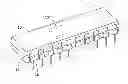
The FIGURE is an isometric view of an exemplary embodiment of an integrated circuit.
DETAILED DESCRIPTION
The disclosure, including the accompanying drawings, is illustrated by way of example and not by way of limitation. It should be noted that references to “an” or “one” embodiment in this disclosure are not necessarily to the same embodiment, and such references mean at least one.
The FIGURE shows an exemplary embodiment of an integrated circuit including a main body 10, a plurality of connection tabs 11 molded on opposite sides of the main body 10, and a plurality of pins 12. The connection tabs 11 and the pins 12 are made of metal. The connection tabs 11 are electrically connected to a logic circuit 13 in the main body 10. The pins 12 are respectively welded on the connection tabs 11.
The contacting area between the connection tabs 11 and the pins 12 is large, so that the pins 12 are not easily broken. Even if one of the pins 12 is broken, the solder of the pin 12 can be melted, and a new pin 12 welded on the corresponding connection tab 11 in its stead.
Even though numerous characteristics and advantages of the embodiments have been set forth in the foregoing description, together with details of the structure and the functions of the embodiments, the disclosure is illustrative only, and changes may be made in details, especially in matters of shape, size, and arrangement of parts within the principles of the embodiments to the full extent indicated by the broad general meaning of the terms in which the appended claims are expressed.
Claims
1. An integrated circuit, comprising:
a main body;
a plurality of connection tabs molded on the main body and exposed outside; and
a plurality of pins respectively connected to the connection tabs;
wherein the connection tabs and the pins are made of metal, the connection tabs are electrically connected to a logic circuit in the main body.
2. The integrated circuit of claim 1, wherein the pins are respectively welded on the connection tabs.
3. The integrated circuit of claim 1, wherein the connection tabs are molded on opposite sides of the main body.
Images & Drawings included:

Sources:
- United States Patent and Trademark Office - verify current appl. status at the USPTO↗
Similar patent applications:
- » 20080104467
Timing failure remedying apparatus for an integrated circuit, timing failure diagnosing apparatus for an integrated circuit, timing failure diagnosing method for an integrated circuit, integrated circuit, computer readable recording medium recorded thereon a timing failure diagnosing program for an integrated circuit, and computer readable recording medium recorded thereon a timing failure remedying program for an integrated circuit - » 20200235091
Integrated circuit chips, integrated circuit packages including the integrated circuit chips, and display apparatuses including the integrated circuit chips - » 20080022252
Method of designing semiconductor integrated circuit, designing apparatus, semiconductor integrated circuit system, semiconductor integrated circuit mounting substrate, package and semiconductor integrated circuit - » 20110012260
METHOD OF DESIGNING SEMICONDUCTOR INTEGRATED CIRCUIT, DESIGNING APPARATUS, SEMICONDUCTOR INTEGRATED CIRCUIT SYSTEM, SEMICONDUCTOR INTEGRATED CIRCUIT MOUNTING SUBSTRATE, PACKAGE AND SEMICONDUCTOR INTEGRATED CIRCUIT - » 20210296287
Integrated circuit chip, method of manufacturing the integrated circuit chip, and integrated circuit package and display apparatus including the integrated circuit chip - » 20200294970
Integrated circuit chip, method of manufacturing the integrated circuit chip, and integrated circuit package and display apparatus including the integrated circuit chip - » 20160141187
METHOD OF MANUFACTURING AN INTEGRATED CIRCUIT WITH IMPRINT, INTEGRATED CIRCUIT WITH IMPRINT, DEVICE FOR FORMING AN INTEGRATED CIRCUIT WITH IMPRINT AND VERIFICATION SYSTEM FOR AN INTEGRATED CIRCUIT WITH IMPRINT - » 20160093549
Integrated circuit heater for reducing stress in the integrated circuit material and chip leads of the integrated circuit, and for optimizing performance of devices of the integrated circuit - » 20110298532
Integrated circuit, integrated circuit design device and integrated circuit design method - » 20130238274
Method for controlling an integrated circuit, integrated circuit and computer including an integrated circuit
Recent applications in this class:
- » 20150061140 2015-03-05
Molded semiconductor package with pluggable lead - » 20140008780 2014-01-09
Semiconductor device housing package, and semiconductor apparatus and electronic apparatus including the same
Recent applications for this Assignee:
- » 20140233961 2014-08-21
Optical communication module including optical-electrical signal converters and optical signal generators - » 20140083669 2014-03-27
HEAT SINK - » 20140063746 2014-03-06
Electronic device with heat dissipation assembly - » 20140061224 2014-03-06
AUTOMATIC VENDING MACHINE - » 20140060914 2014-03-06
Enclosure with shield apparatus - » 20140058727 2014-02-27
MULTIMEDIA RECORDING SYSTEM AND METHOD - » 20140055955 2014-02-27
Fastener - » 20140055322 2014-02-27
DISPLAY SYSTEM AND HEAD-MOUNTED DISPLAY APPARATUS - » 20140054439 2014-02-27
CONTAINER DATA CENTER WITH SUPPORTING APPARATUS - » 20140054311 2014-02-27
AUTOMATIC VENDING MACHINE WITH MOVING MEMBER FOR PRODUCTS