Semiconductor package, semiconductor device using the same and manufacturing method thereof
US20170194227A1
2017-07-06
15/342,138
2016-11-03
✅ Patent granted
US 10,242,927 B2
2019-03-26
-
-
Niki H Nguyen
Wolf, Greenfield & Sacks, P.C.
2036-11-03
Abstract:
A semiconductor package includes a substrate, a first electronic component, a film and a package body. The first electronic component is disposed on the substrate and has an upper surface. The film is disposed on the upper surface of the first electronic component. The package body encapsulates the first electronic component and the film.
Inventors:
- Wen-Sung HSU 36 🇹🇼 Zhubei City, Taiwan
- Shih-Chin LIN 11 🇹🇼 Taoyuan City, Taiwan
- Ming-Jen HSIUNG 3 🇹🇼 Zhubei City, Taiwan
- Wen-Sung Hsu 34 🇹🇼 Zhubei, Taiwan
- Shih-Chin Lin 10 🇹🇼 Taoyuan, Taiwan
- Ming-Jen Hsiung 3 🇹🇼 Zhubei, Taiwan
Assignee:
- MEDIATEK INC. 3,761 🇹🇼 Hsin-Chu, Taiwan
Applicant:
Interested in similar patents?
Get notified when new applications in this technology area are published.
Classification:
H01L25/0657 » CPC further
Assemblies consisting of a plurality of individual semiconductor or other solid state devices ; Multistep manufacturing processes thereof all the devices being of a type provided for in the same subgroup of groups - , e.g. assemblies of rectifier diodes the devices not having separate containers the devices being of a type provided for in group Stacked arrangements of devices
H01L23/3128 » CPC main
Details of semiconductor or other solid state devices; Encapsulations, e.g. encapsulating layers, coatings, e.g. for protection characterised by the arrangement or shape the device being completely enclosed a substrate forming part of the encapsulation the substrate having spherical bumps for external connection
H01L23/3135 » CPC further
Details of semiconductor or other solid state devices; Encapsulations, e.g. encapsulating layers, coatings, e.g. for protection characterised by the arrangement or shape the device being completely enclosed Double encapsulation or coating and encapsulation
H01L21/78 » CPC further
Processes or apparatus adapted for the manufacture or treatment of semiconductor or solid state devices or of parts thereof; Manufacture or treatment of devices consisting of a plurality of solid state components formed in or on a common substrate or of parts thereof; Manufacture of integrated circuit devices or of parts thereof; Manufacture or treatment of devices consisting of a plurality of solid state components or integrated circuits formed in, or on, a common substrate with subsequent division of the substrate into plural individual devices
H01L21/304 » CPC further
Processes or apparatus adapted for the manufacture or treatment of semiconductor or solid state devices or of parts thereof; Manufacture or treatment of semiconductor devices or of parts thereof the devices having at least one potential-jump barrier or surface barrier, e.g. PN junction, depletion layer or carrier concentration layer the devices having semiconductor bodies comprising elements of Group IV of the Periodic System or AB compounds with or without impurities, e.g. doping materials; Treatment of semiconductor bodies using processes or apparatus not provided for in groups - to change their surface-physical characteristics or shape, e.g. etching, polishing, cutting Mechanical treatment, e.g. grinding, polishing, cutting
H01L23/498 IPC
Details of semiconductor or other solid state devices; Arrangements for conducting electric current to or from the solid state body in operation, e.g. leads, terminal arrangements ; Selection of materials therefor consisting of soldered constructions Leads, on insulating substrates,
H01L23/49822 » CPC further
Details of semiconductor or other solid state devices; Arrangements for conducting electric current to or from the solid state body in operation, e.g. leads, terminal arrangements ; Selection of materials therefor consisting of soldered constructions; Leads, on insulating substrates, Multilayer substrates
H01L23/49827 » CPC further
Details of semiconductor or other solid state devices; Arrangements for conducting electric current to or from the solid state body in operation, e.g. leads, terminal arrangements ; Selection of materials therefor consisting of soldered constructions; Leads, on insulating substrates, Via connections through the substrates, e.g. pins going through the substrate, coaxial cables
H01L23/49838 » CPC further
Details of semiconductor or other solid state devices; Arrangements for conducting electric current to or from the solid state body in operation, e.g. leads, terminal arrangements ; Selection of materials therefor consisting of soldered constructions; Leads, on insulating substrates, Geometry or layout
H01L23/562 » CPC further
Details of semiconductor or other solid state devices Protection against mechanical damage
H01L2225/06517 » CPC further
Details relating to assemblies covered by the group but not provided for in its subgroups; All the devices being of a type provided for in the same subgroup of groups - the devices not having separate containers the devices being of a type provided for in group; Stacked arrangements of devices Bump or bump-like direct electrical connections from device to substrate
H01L2225/06548 » CPC further
Details relating to assemblies covered by the group but not provided for in its subgroups; All the devices being of a type provided for in the same subgroup of groups - the devices not having separate containers the devices being of a type provided for in group; Stacked arrangements of devices Conductive via connections through the substrate, container, or encapsulation
H01L23/31 IPC
Details of semiconductor or other solid state devices; Encapsulations, e.g. encapsulating layers, coatings, e.g. for protection characterised by the arrangement or shape
H01L23/00 IPC
Details of semiconductor or other solid state devices
H01L25/065 IPC
Assemblies consisting of a plurality of individual semiconductor or other solid state devices ; Multistep manufacturing processes thereof all the devices being of a type provided for in the same subgroup of groups - , e.g. assemblies of rectifier diodes the devices not having separate containers the devices being of a type provided for in group
H01L21/56 » CPC further
Processes or apparatus adapted for the manufacture or treatment of semiconductor or solid state devices or of parts thereof; Manufacture or treatment of semiconductor devices or of parts thereof the devices having at least one potential-jump barrier or surface barrier, e.g. PN junction, depletion layer or carrier concentration layer; Assembly of semiconductor devices using processes or apparatus not provided for in a single one of the subgroups - , e.g. sealing of a cap to a base of a container Encapsulations, e.g. encapsulation layers, coatings
H01L24/94 » CPC further
Arrangements for connecting or disconnecting semiconductor or solid-state bodies; Methods or apparatus related thereto; Batch processes at wafer-level, i.e. with connecting carried out on a wafer comprising a plurality of undiced individual devices
H01L24/13 » CPC further
Arrangements for connecting or disconnecting semiconductor or solid-state bodies; Methods or apparatus related thereto; Means for bonding being attached to, or being formed on, the surface to be connected, e.g. chip-to-package, die-attach, "first-level" interconnects; Manufacturing methods related thereto; Bump connectors ; Manufacturing methods related thereto; Structure, shape, material or disposition of the bump connectors prior to the connecting process of an individual bump connector
H01L24/48 » CPC further
Arrangements for connecting or disconnecting semiconductor or solid-state bodies; Methods or apparatus related thereto; Means for bonding being attached to, or being formed on, the surface to be connected, e.g. chip-to-package, die-attach, "first-level" interconnects; Manufacturing methods related thereto; Wire connectors; Manufacturing methods related thereto; Structure, shape, material or disposition of the wire connectors after the connecting process of an individual wire connector
H01L2224/73153 » CPC further
Indexing scheme for arrangements for connecting or disconnecting semiconductor or solid-state bodies and methods related thereto as covered by; Means for bonding being of different types provided for in two or more of groups; Location prior to the connecting process on different surfaces Bump and layer connectors
H01L2224/94 » CPC further
Indexing scheme for arrangements for connecting or disconnecting semiconductor or solid-state bodies and methods related thereto as covered by; Batch processes at wafer-level, i.e. with connecting carried out on a wafer comprising a plurality of undiced individual devices
H01L2225/1058 » CPC further
Details relating to assemblies covered by the group but not provided for in its subgroups; All the devices being of a type provided for in the same subgroup of groups - the devices having separate containers the devices being of a type provided for in group the containers being in a stacked arrangement; Details of electrical connections between containers Bump or bump-like electrical connections, e.g. balls, pillars, posts
H01L2924/00014 » CPC further
Indexing scheme for arrangements or methods for connecting or disconnecting semiconductor or solid-state bodies as covered by; Technical content checked by a classifier the subject-matter covered by the group, the symbol of which is combined with the symbol of this group, being disclosed without further technical details
H01L2924/1533 » CPC further
Indexing scheme for arrangements or methods for connecting or disconnecting semiconductor or solid-state bodies as covered by; Details of package parts other than the semiconductor or other solid state devices to be connected; Die mounting substrate; Connection portion the connection portion being formed on the die mounting surface of the substrate the connection portion being formed both on the die mounting surface of the substrate and outside the die mounting surface of the substrate
H01L2924/15321 » CPC further
Indexing scheme for arrangements or methods for connecting or disconnecting semiconductor or solid-state bodies as covered by; Details of package parts other than the semiconductor or other solid state devices to be connected; Die mounting substrate; Connection portion the connection portion being formed on the die mounting surface of the substrate being a ball array, e.g. BGA
H01L2924/15331 » CPC further
Indexing scheme for arrangements or methods for connecting or disconnecting semiconductor or solid-state bodies as covered by; Details of package parts other than the semiconductor or other solid state devices to be connected; Die mounting substrate; Connection portion the connection portion being formed on the die mounting surface of the substrate the connection portion being formed both on the die mounting surface of the substrate and outside the die mounting surface of the substrate being a ball array, e.g. BGA
H01L2924/1815 » CPC further
Indexing scheme for arrangements or methods for connecting or disconnecting semiconductor or solid-state bodies as covered by; Details of package parts other than the semiconductor or other solid state devices to be connected; Encapsulation Shape
H01L2924/19041 » CPC further
Indexing scheme for arrangements or methods for connecting or disconnecting semiconductor or solid-state bodies as covered by; Details of hybrid assemblies other than the semiconductor or other solid state devices to be connected; Structure; Component type being a capacitor
H01L2924/19042 » CPC further
Indexing scheme for arrangements or methods for connecting or disconnecting semiconductor or solid-state bodies as covered by; Details of hybrid assemblies other than the semiconductor or other solid state devices to be connected; Structure; Component type being an inductor
H01L2924/19043 » CPC further
Indexing scheme for arrangements or methods for connecting or disconnecting semiconductor or solid-state bodies as covered by; Details of hybrid assemblies other than the semiconductor or other solid state devices to be connected; Structure; Component type being a resistor
H01L2924/19105 » CPC further
Indexing scheme for arrangements or methods for connecting or disconnecting semiconductor or solid-state bodies as covered by; Details of hybrid assemblies other than the semiconductor or other solid state devices to be connected; Disposition of discrete passive components in a side-by-side arrangement on a common die mounting substrate
H01L2924/3512 » CPC further
Indexing scheme for arrangements or methods for connecting or disconnecting semiconductor or solid-state bodies as covered by; Technical effects; Mechanical effects; Thermal stress Cracking
H01L24/16 » CPC further
Arrangements for connecting or disconnecting semiconductor or solid-state bodies; Methods or apparatus related thereto; Means for bonding being attached to, or being formed on, the surface to be connected, e.g. chip-to-package, die-attach, "first-level" interconnects; Manufacturing methods related thereto; Bump connectors ; Manufacturing methods related thereto; Structure, shape, material or disposition of the bump connectors after the connecting process of an individual bump connector
H01L2924/15311 » CPC further
Indexing scheme for arrangements or methods for connecting or disconnecting semiconductor or solid-state bodies as covered by; Details of package parts other than the semiconductor or other solid state devices to be connected; Die mounting substrate; Connection portion the connection portion being formed only on the surface of the substrate opposite to the die mounting surface being a ball array, e.g. BGA
H01L2225/1023 » CPC further
Details relating to assemblies covered by the group but not provided for in its subgroups; All the devices being of a type provided for in the same subgroup of groups - the devices having separate containers the devices being of a type provided for in group the containers being in a stacked arrangement the lowermost container comprising a device support the support being an insulating substrate
Description
This application claims the benefit of U.S. Provisional application Ser. No. 62/273,478, filed Dec. 31, 2015, the disclosure of which is incorporated by reference herein in its entirety.
FIELD OF THE INVENTION
The invention relates to a semiconductor package, a semiconductor device using the same and a manufacturing method thereof, and more particularly to a semiconductor package having a film, a semiconductor device using the same and a manufacturing method thereof.
BACKGROUND OF THE INVENTION
In the electronics industry, high integration and multiple functions with high performance become essential for new products. And meanwhile, high integration may cause higher manufacturing cost, since the manufacturing cost is in proportional to its size. Therefore, demanding on miniaturization of integrated circuit (IC) packages has become more and more critical. Package-on-package (PoP) is now the fastest growing semiconductor package technology since it is a cost-effective solution to high-density system integration in a single package. However, since the PoP structure has a thin thickness, the PoP structure is easy to crack or damage due to heating or other factors.
Therefore, it is important to solve or improve the above problem.
SUMMARY OF THE INVENTION
In one embodiment of the invention, a semiconductor package is provided. The semiconductor package includes a substrate, a first electronic component, a film and a package body. The first electronic component is disposed on the substrate and has an upper surface. The film is disposed on the upper surface of the first electronic component. The package body encapsulates the first electronic component and the film.
In another embodiment of the invention, a semiconductor device is provided. The semiconductor device includes a semiconductor package and a second electronic component. The semiconductor package includes a substrate, a first electronic component, a film and a package body. The first electronic component is disposed on the substrate and has an upper surface. The film is disposed on the upper surface of the first electronic component. The package body encapsulates the first electronic component and the film. The second electronic component is stacked to the semiconductor package.
In another embodiment of the invention, a manufacturing method of a semiconductor package is provided. The manufacturing method includes the following steps. A wafer having an upper surface is provided; a film is disposed on the upper surface of the wafer; a singulation path passing through the wafer and the film is formed to form at least one first electronic component on which the film is disposed; a substrate is provided; first electronic component is disposed on the substrate; and a package body encapsulating the first electronic component and the film is formed.
Numerous objects, features and advantages of the invention will be readily apparent upon a reading of the following detailed description of embodiments of the invention when taken in conjunction with the accompanying drawings. However, the drawings employed herein are for the purpose of descriptions and should not be regarded as limiting.
BRIEF DESCRIPTION OF THE DRAWINGS
The above objects and advantages of the invention will become more readily apparent to those ordinarily skilled in the art after reviewing the following detailed description and accompanying drawings, in which:
FIG. 1 illustrates a diagram of a semiconductor package according to an embodiment of the invention;
FIG. 2 illustrates a diagram of a semiconductor package according to another embodiment of the invention;
FIG. 3 illustrates a diagram of a semiconductor device according to an embodiment of the invention; and
FIGS. 4A to 4G illustrate manufacturing processes of the semiconductor package 100 of FIG. 1.
DETAILED DESCRIPTION OF PREFERRED EMBODIMENTS
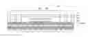
FIG. 1 illustrates a diagram of a semiconductor package 100 according to an embodiment of the invention. The semiconductor package 100 includes a substrate 110, at least one first electronic component 120, at least one first conductive contact 130, at least one second conductive contact 135, a package body 140 and a film 150.
The substrate 110 is, for example, a multi-layered structure or single-layered structure. The substrate 110 may be an organic substrate, a ceramic substrate, a silicon substrate, a metal substrate, etc. In another embodiment, the substrate 110 may be an interposer or a wafer having at least one redistribution layer (RDL).
The first electronic component 120 is disposed on the substrate 110 and has an upper surface 120u. In the present embodiment, the first electronic component 120 is coupled to an upper surface 110u of the substrate 110 in a “face-down” orientation and electrically connected to the substrate 110 via a plurality of conductive contacts 121. This configuration is sometimes referred to as “flip-chip”. The conductive contact 121 may be a solder ball, a conductive pillar, etc.
In other embodiments, the first electronic component 120 may be coupled to the substrate 110 in a “face-up” orientation, and electrically connected to the substrate 110 via a plurality of conductive bond wires (not shown). The first electronic component 120 may be an active chip or a passive component, such as a resistor, an inductor or a capacitor. In another embodiment, the number of the first electronic component 120 may be several.
The first conductive contacts 130 are disposed on the upper surface 110u of the substrate 110 and surround the first electronic component 120. The first conductive contacts 130 are exposed from the package body 140 for being electrically connected to an exterior electronic component (not illustrated). For example, a portion of each first conductive contact 130 is encapsulated by the package body 140 and another portion of each first conductive contact 130 is exposed from the package body 140 for being electrically connected to the exterior electronic component. In addition, the first conductive contacts 130 may be solder balls, conductive pillars, etc.
The second conductive contacts 135 are disposed on a lower surface 110b of the substrate 110. The semiconductor package 100 may be disposed on and electrically connected to an exterior circuit, such as a circuit board, through the second conductive contacts 135. The second conductive contacts 135 may be solder balls, conductive pillars, etc.
The package body 140 encapsulates the first electronic component 120, the film 150 and a portion of each first conductive contact 130. In the present embodiment, the package body 140 covers an upper surface 150u of the film 150. In another embodiment, the package body 140 may expose the upper surface 150u of the film 150 and covers a lateral surface of the film 150.
The package body 140 includes a covering portion 141 covering the upper surface 150u of the film 150. The film 150 has a first thickness T1 being equal to or less than a second thickness T2 of the covering portion 141. As a result, it can increase the strength of the package body 140 to prevent the package body 140 from cracking in the interface between the first electronic component 120 and the package body 140.
The package body 140 may be made of the same material. For example, the package body 140 is a molding compound which is made of a material including, for example, a Novolac-based resin, an epoxy-based resin, a silicone-based resin, or another suitable encapsulant. Suitable fillers also can be included, such as powdered SiO2.
The film 150 is disposed on the upper surface 120u of the first electronic component 120. The film 150 can increase the strength of the interface between the first electronic component 120 and the package body 140 and accordingly it can prevent the package body 140 from cracking in interface between the first electronic component 120 and the package body 140. In addition, the film 150 has an adhesion conducive to fixing the package body 140 to the first electronic component 120, and accordingly it can increase the adhesion between the film 150 and the package body 140 and the adhesion between the film 150 and the first electronic component 120. In addition, the film 150 may be made of epoxy resin, acrylate resin or combination thereof.
In the present embodiment, the film 150 is directly adhered to the upper surface 120u of the first electronic component 120. In another embodiment, the film 150 may be indirectly adhered to the upper surface 120u of the first electronic component 120 by any layer structure, such as an adhesion.
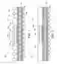
FIG. 2 illustrates a diagram of a semiconductor package 200 according to another embodiment of the invention. The semiconductor package 200 includes the substrate 110, at least one first electronic component 120, at least one second conductive contact 135, the package body 140 and the film 150. Compared to the semiconductor package 100, the semiconductor package 200 may omit the first conductive contacts 130.
FIG. 3 illustrates a diagram of a semiconductor device 10 according to an embodiment of the invention. The semiconductor device 10 includes the semiconductor package 100 and at least one second electronic component 11.
The second electronic component 11 may be, for example, a memory, a semiconductor component rather than memory, another semiconductor package, an active component, a passive component, etc. In another embodiment, the second electronic component 11 may be a semiconductor package including a plurality of dies, such as DRAMs stacked to each other.
The second electronic component 11 is stacked to the package body 140 of the semiconductor package 100 in a “face-down” orientation or in a “face-up” orientation. The second electronic component 11 is electrically connected to the first conductive contacts 130 of the semiconductor package 100 via a plurality of conductive contacts 12, such that second electronic component 11 may be electrically to the first electronic component 120 through the conductive contacts 12, the first conductive contacts 130 and the substrate 110. This configuration is sometimes referred to as “flip-chip”. The conductive contacts 12 may be solder balls, conductive pillars, etc.
In other embodiments, the second electronic component 11 may be stacked to the semiconductor package 100 in a “face-up” orientation, and electrically connected to the first conductive contacts 130 via a plurality of conductive bond wires (not shown).
Due to the film 150 being disposed on the first electronic component 120 to increase the strength the interface between the first electronic component 120 and the package body 140, even if the second electronic component 11 is removed from the semiconductor package 100 by heating, the first electronic component 120 and/or the package body 140 is not easy to crack or damage.
FIGS. 4A to 4G illustrate manufacturing processes of the semiconductor package 100 of FIG. 1.
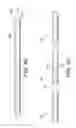
Referring to FIG. 4A, a wafer 120′ is provided, wherein the wafer 120′ has at least one circuit (not illustrated). Then, the upper surface 120u of the wafer 120′ may be grinded for enhancing die strength.
Referring to FIG. 4B, the film 150 is adhered to the wafer 120′ and the conductive contacts 121s are disposed on the wafer 120′. In an embodiment, the film 150 is adhered to the wafer 120′ first, and then the conductive contacts 121s are disposed on the wafer 120′. In another embodiment, the conductive contacts 121s are disposed on the wafer 120′ first, and then the film 150 is adhered to the wafer 120′. In addition, the film 150 may be heated to be solidified.
Referring to FIG. 4C, at least one singulation path P1 passing through the wafer 120′ and the film 150 to form at least one first electronic component 120 on which the film 150 is disposed. The singulation path P1 may be formed by using, for example, laser or saw, etc.
Referring to FIG. 4D, the substrate 110 is provided. The substrate 110 is, for example, a multi-layered structure or single-layered structure. The substrate 110 may be an organic substrate, a ceramic substrate, a silicon substrate, a metal substrate, etc. In another embodiment, the substrate 110 may be an interposer or a wafer having at least one redistribution layer (RDL).
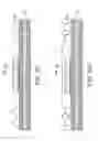
Referring to FIG. 4E, the first conductive contacts 130 are formed on the upper surface 110u of the substrate 110 by using, for example, SMT (surface-mount technology).
Referring to FIG. 4F, the first electronic component 120 with the film 150 is disposed on the substrate 110, wherein the first conductive contacts 130 surround the first electronic component 120.
Referring to FIG. 4G, the package body 140 encapsulating the first electronic component 120, the film 150 and a portion of the each first conductive contact 130 is formed, wherein another portion of each first conductive contact 130 is exposed from the package body 140. The package body 140 may be formed by various packaging technologies, such as, for example, compression molding, injection molding, transfer molding or dispensing technology.
Then, the second conductive contacts 135 of FIG. 1 are formed on the lower surface 110b of the substrate 110 using, for example, ball mounting technology, to form the semiconductor package 100 of FIG. 1.
In another embodiment, the forming of the first conductive contacts 130 may be omitted to from the semiconductor package 200 of FIG. 2.
In addition, the second electronic component 11 of FIG. 3 may be disposed above the package body 140 of FIG. 1 by using SMT to form the semiconductor device 10 of FIG. 3.
While the invention has been described in terms of what is presently considered to be the most practical and preferred embodiments, it is to be understood that the invention needs not be limited to the disclosed embodiment. On the contrary, it is intended to cover various modifications and similar arrangements included within the spirit and scope of the appended claims which are to be accorded with the broadest interpretation so as to encompass all such modifications and similar structures.
Claims
What is claimed is:1. A semiconductor package, comprising:
a substrate;
a first electronic component disposed on the substrate and having an upper surface;
a film disposed on the upper surface of the first electronic component; and
a package body encapsulating the first electronic component and the film.
2. The semiconductor package as claimed in claim 1, wherein the film is directly adhered to the upper surface of the first electronic component.
3. The semiconductor package as claimed in claim 1, wherein the package body covers an upper surface of the film.
4. The semiconductor package as claimed in claim 1, wherein an upper surface of the film is exposed from the package body.
5. The semiconductor package as claimed in claim 1, wherein the package body further comprises a covering portion covering an upper surface of the film, and the film has a first thickness less than a second thickness of the covering portion.
6. The semiconductor package as claimed in claim 1, further comprising:
a plurality of conductive components disposed on the substrate and surrounding the first electronic component;
wherein a portion of each conductive component is encapsulated by the package body and another portion of each conductive component is exposed from the package body.
7. A semiconductor device, comprising:
a semiconductor package as claimed in claim 1; and
a second electronic component stacked to the semiconductor package.
8. The semiconductor device as claimed in claim 7, wherein the film is directly adhered to the upper surface of the first electronic component.
9. The semiconductor device as claimed in claim 7, wherein the package body covers an upper surface of the film.
10. The semiconductor device as claimed in claim 7, wherein an upper surface of the film is exposed from the package body.
11. The semiconductor device as claimed in claim 7, wherein the package body further comprises a covering portion covering an upper surface of the film, and the film has a first thickness less than a second thickness of the covering portion.
12. The semiconductor device as claimed in claim 7, wherein the semiconductor package further comprises:
a plurality of conductive components disposed on the substrate and surrounding the first electronic component;
wherein a portion of each conductive component is encapsulated by the package body and another portion of each conductive component is exposed from the package body.
13. A manufacturing method of a semiconductor package, comprising:
providing a wafer having an upper surface;
disposing a film on the upper surface of the wafer;
forming a singulation path passing through the wafer and the film to form at least one first electronic component on which the film is disposed;
providing a substrate;
disposing the first electronic component on the substrate; and
forming a package body encapsulating the first electronic component and the film.
14. The manufacturing method as claimed in claim 13, further comprises:
grinding the upper surface of the wafer.
15. The manufacturing method as claimed in claim 13, further comprises:
heating the film to solidify the film.
Images & Drawings included:


Sources:
- United States Patent and Trademark Office - verify current appl. status at the USPTO↗
Similar patent applications:
- » 20170084541
Semiconductor package, semiconductor device using the same and manufacturing method thereof - » 20070045859
Semiconductor device, semiconductor package for use therein, and manufacturing method thereof - » 20080230924
Semiconductor device, semiconductor package for use therein, and manufacturing method thereof - » 20100140787
Semiconductor device, semiconductor package for use therein, and manufacturing method thereof - » 20150221843
Semiconductor light emitting device, manufacturing method thereof, and semiconductor light emitting device package using the same - » 10690627
Semiconductor device, semiconductor package for use therein, and manufacturing method thereof - » 20170040292
Semiconductor package, semiconductor device using the same and manufacturing method thereof - » 20240118491
PHOTONIC SEMICONDUCTOR DEVICE, PHOTONIC SEMICONDUCTOR PACKAGE USING THE SAME AND MANUFACTURING METHOD THEREOF - » 20170136582
Composite solder ball, semiconductor package using the same, semiconductor device using the same and manufacturing method thereof - » 20160263709
Composite solder ball, semiconductor package using the same, semiconductor device using the same and manufacturing method thereof
Recent applications in this class:
- » 20250273526 2025-08-28
FULLY MOLDED STRUCTURE WITH MULTI-HEIGHT COMPONENTS COMPRISING BACKSIDE CONDUCTIVE MATERIAL AND METHOD FOR MAKING THE SAME - » 20250266313 2025-08-21
SEMICONDUCTOR DEVICE PACKAGE AND METHOD OF MANUFACTURING THE SAME - » 20250233035 2025-07-17
SEMICONDUCTOR DEVICE AND METHOD OF MANUFACTURING A SEMICONDUCTOR DEVICE - » 20250210432 2025-06-26
ELECTRONIC PACKAGE AND MANUFACTURING METHOD THEREOF - » 20250201645 2025-06-19
FABRICATING PACKAGES WITH DUMMY DIES HAVING A CONSTRUCTION THAT MIMICS WARPAGE OF THE OTHER COMPONENTS INCLUDED IN THE PACKAGE - » 20250191990 2025-06-12
MANUFACTURING METHOD OF SEMICONDUCTOR PACKAGE - » 20250191989 2025-06-12
PACKAGE COMPRISING A SUBSTRATE WITH CAVITY AND AN INTEGRATED DEVICE WITH A STEP BACK SIDE - » 20250157870 2025-05-15
PACKAGE STRUCTURES - » 20250118609 2025-04-10
Semiconductor Packages and Methods of Forming - » 20250079248 2025-03-06
SEMICONDUCTOR PACKAGE AND METHOD OF MANUFACTURING SEMICONDUCTOR PACKAGE
Recent applications for this Assignee:
- » 20250274873 2025-08-28
METHOD AND APPARATUS OF PERFORMING POWER CONTROL ON WIRELESS COMMUNICATION DEVICE WITH POWER ESTIMATION CALIBRATION AND RELATED WIRELESS COMMUNICATION DEVICE - » 20250274501 2025-08-28
VIDEO TRANSMISSION METHOD THROUGH DYNAMIC DISPATCHING MPDUS AMONG MULTI-LINKS - » 20250266617 2025-08-21
ANTENNA INCLUDING CONDUCTIVE PLATES AND CONDUCTIVE LOOPS AND CAPABLE OF REDUCING SPURIOUS EMISSIONS - » 20250247505 2025-07-31
IMAGE PROCESSING SYSTEM AND IMAGE PROCESSING METHOD - » 20250233905 2025-07-17
Multimedia System with Dynamic Adaptation - » 20250233593 2025-07-17
Counter System and Method of Driving the Counter System with Zero Accumulated Error - » 20250227077 2025-07-10
Router-Bridge Capable of Fast Exchanging Network Packets - » 20250225301 2025-07-10
METHOD FOR PERFORMING BLOCK LEVEL EXPLORATION OF INTEGRATED CIRCUIT DESIGN, ASSOCIATED ELECTRONIC DEVICE AND ASSOCIATED COMPUTER-READABLE MEDIUM - » 20250224888 2025-07-10
APPARATUS AND METHOD FOR HANDLING SUDDEN POWER LOSS OF STORAGE DEVICE - » 20250224442 2025-07-10
Dynamic Voltage Stress Condition Optimization Method and Dynamic Voltage Stress Condition Optimization System Capable of Performing Block-based Dynamic Voltage Stress Wafer Testing Process