Arrangement with a semiconductor chip and support therefore and method for a bonded wire connection
US20050127497A1
2005-06-16
11/039,284
2005-01-20
✅ Patent granted
US 7,053,489 B2
2006-05-30
-
-
Nathan J. Flynn | Kevin Quinto
2025-01-20
Abstract:
The invention relates to an assembly comprising a support, which bears a semiconductor chip that is connected to a metallized surface on the rear of the support by means of a through-plating. A first nail head contact, from which the connection wire has been separated, is formed on the through-plating. A second nail head contact is formed on a connection pad of the semiconductor chip. The wire that connects the semiconductor to the through-plating runs from said second nail head contact to the first nail head contact and is connected to the latter by means of a wedge contact.
Assignee:
- SIEMENS AKTIENGESELLSCHAFT 12,417 🇩🇪 Munich, Germany
Interested in similar patents?
Get notified when new applications in this technology area are published.
Classification:
H01L23/48 IPC
Details of semiconductor or other solid state devices Arrangements for conducting electric current to or from the solid state body in operation, e.g. leads, terminal arrangements ; Selection of materials therefor
H01L24/85 » CPC main
Arrangements for connecting or disconnecting semiconductor or solid-state bodies; Methods or apparatus related thereto; Methods for connecting semiconductor or other solid state bodies using means for bonding being attached to, or being formed on, the surface to be connected using a wire connector
H01L21/486 » CPC further
Processes or apparatus adapted for the manufacture or treatment of semiconductor or solid state devices or of parts thereof; Manufacture or treatment of semiconductor devices or of parts thereof the devices having at least one potential-jump barrier or surface barrier, e.g. PN junction, depletion layer or carrier concentration layer; Manufacture or treatment of parts, e.g. containers, prior to assembly of the devices, using processes not provided for in a single one of the subgroups -; Conductive parts; Leads on or in insulating or insulated substrates, e.g. metallisation Via connections through the substrate with or without pins
H01L24/48 » CPC further
Arrangements for connecting or disconnecting semiconductor or solid-state bodies; Methods or apparatus related thereto; Means for bonding being attached to, or being formed on, the surface to be connected, e.g. chip-to-package, die-attach, "first-level" interconnects; Manufacturing methods related thereto; Wire connectors; Manufacturing methods related thereto; Structure, shape, material or disposition of the wire connectors after the connecting process of an individual wire connector
H05K3/328 » CPC further
Apparatus or processes for manufacturing printed circuits; Assembling printed circuits with electric components, e.g. with resistor electrically connecting electric components or wires to printed circuits by welding
H05K3/328 » CPC further
Apparatus or processes for manufacturing printed circuits; Assembling printed circuits with electric components, e.g. with resistor electrically connecting electric components or wires to printed circuits by welding
H05K3/4015 » CPC further
Apparatus or processes for manufacturing printed circuits; Forming printed elements for providing electric connections to or between printed circuits; Surface contacts, e.g. bumps using auxiliary conductive elements, e.g. pieces of metal foil, metallic spheres
H05K3/4015 » CPC further
Apparatus or processes for manufacturing printed circuits; Forming printed elements for providing electric connections to or between printed circuits; Surface contacts, e.g. bumps using auxiliary conductive elements, e.g. pieces of metal foil, metallic spheres
H01L24/45 » CPC further
Arrangements for connecting or disconnecting semiconductor or solid-state bodies; Methods or apparatus related thereto; Means for bonding being attached to, or being formed on, the surface to be connected, e.g. chip-to-package, die-attach, "first-level" interconnects; Manufacturing methods related thereto; Wire connectors; Manufacturing methods related thereto; Structure, shape, material or disposition of the wire connectors prior to the connecting process of an individual wire connector
H01L24/78 » CPC further
Arrangements for connecting or disconnecting semiconductor or solid-state bodies; Methods or apparatus related thereto; Apparatus for manufacturing arrangements for connecting or disconnecting semiconductor or solid-state bodies Apparatus for connecting with wire connectors
H01L2224/85051 » CPC further
Indexing scheme for arrangements for connecting or disconnecting semiconductor or solid-state bodies and methods related thereto as covered by; Methods for connecting semiconductor or other solid state bodies using means for bonding being attached to, or being formed on, the surface to be connected using a wire connector; Pre-treatment of the connector or the bonding area Forming additional members, e.g. for "wedge-on-ball", "ball-on-wedge", "ball-on-ball" connections
H01L2924/01013 » CPC further
Indexing scheme for arrangements or methods for connecting or disconnecting semiconductor or solid-state bodies as covered by; Chemical elements Aluminum [Al]
H01L2924/01027 » CPC further
Indexing scheme for arrangements or methods for connecting or disconnecting semiconductor or solid-state bodies as covered by; Chemical elements Cobalt [Co]
H01L2924/01032 » CPC further
Indexing scheme for arrangements or methods for connecting or disconnecting semiconductor or solid-state bodies as covered by; Chemical elements Germanium [Ge]
H01L2924/01033 » CPC further
Indexing scheme for arrangements or methods for connecting or disconnecting semiconductor or solid-state bodies as covered by; Chemical elements Arsenic [As]
H01L2924/01068 » CPC further
Indexing scheme for arrangements or methods for connecting or disconnecting semiconductor or solid-state bodies as covered by; Chemical elements Erbium [Er]
H01L2924/01078 » CPC further
Indexing scheme for arrangements or methods for connecting or disconnecting semiconductor or solid-state bodies as covered by; Chemical elements Platinum [Pt]
H01L2924/01079 » CPC further
Indexing scheme for arrangements or methods for connecting or disconnecting semiconductor or solid-state bodies as covered by; Chemical elements Gold [Au]
H05K1/113 » CPC further
Printed circuits; Details; Printed elements for providing electric connections to or between printed circuits; Pads for surface mounting, e.g. lay-out directly combined with via connections Via provided in pad; Pad over filled via
H05K1/113 » CPC further
Printed circuits; Details; Printed elements for providing electric connections to or between printed circuits; Pads for surface mounting, e.g. lay-out directly combined with via connections Via provided in pad; Pad over filled via
H05K2203/049 » CPC further
Indexing scheme relating to apparatus or processes for manufacturing printed circuits covered by; Soldering or other types of metallurgic bonding Wire bonding
H05K2203/049 » CPC further
Indexing scheme relating to apparatus or processes for manufacturing printed circuits covered by; Soldering or other types of metallurgic bonding Wire bonding
H01L2224/78301 » CPC further
Indexing scheme for arrangements for connecting or disconnecting semiconductor or solid-state bodies and methods related thereto as covered by; Apparatus for manufacturing arrangements for connecting or disconnecting semiconductor or solid-state bodies and for methods related thereto; Apparatus for connecting with wire connectors; Means for applying energy, e.g. heating means by means of pressure Capillary
H01L2224/85205 » CPC further
Indexing scheme for arrangements for connecting or disconnecting semiconductor or solid-state bodies and methods related thereto as covered by; Methods for connecting semiconductor or other solid state bodies using means for bonding being attached to, or being formed on, the surface to be connected using a wire connector; Applying energy for connecting; Compression bonding Ultrasonic bonding
H01L2924/00 » CPC further
Indexing scheme for arrangements or methods for connecting or disconnecting semiconductor or solid-state bodies as covered by
H01L2924/00015 » CPC further
Indexing scheme for arrangements or methods for connecting or disconnecting semiconductor or solid-state bodies as covered by; Technical content checked by a classifier the subject-matter covered by the group, the symbol of which is combined with the symbol of this group, being disclosed as prior art
H01L2224/85399 » CPC further
Indexing scheme for arrangements for connecting or disconnecting semiconductor or solid-state bodies and methods related thereto as covered by; Methods for connecting semiconductor or other solid state bodies using means for bonding being attached to, or being formed on, the surface to be connected using a wire connector; Bonding interfaces outside the semiconductor or solid-state body Material
H01L2924/00014 » CPC further
Indexing scheme for arrangements or methods for connecting or disconnecting semiconductor or solid-state bodies as covered by; Technical content checked by a classifier the subject-matter covered by the group, the symbol of which is combined with the symbol of this group, being disclosed without further technical details
H01L2224/05599 » CPC further
Indexing scheme for arrangements for connecting or disconnecting semiconductor or solid-state bodies and methods related thereto as covered by; Means for bonding being attached to, or being formed on, the surface to be connected, e.g. chip-to-package, die-attach, "first-level" interconnects; Manufacturing methods related thereto; Bonding areas; Manufacturing methods related thereto; Structure, shape, material or disposition of the bonding areas prior to the connecting process of an individual bonding area; External layer Material
Description
CROSS-REFERENCE TO RELATED APPLICATION OR PRIORITYThis application is a continuation of co-pending International Application No. PCT/DE03/02465 filed Jul. 22, 2003 which designates the United States, and claims priority to German application number DE10233607.5 filed Jul. 24, 2002.
FIELD OF THE INVENTIONThe invention is directed to an arrangement with a semiconductor chip, a support with through-plating, and a wire connecting a contact pad of the semiconductor chip to the through-plating and method for producing such an arrangement.
The invention relates to an arrangement with a semiconductor chip and a support provided with a contact point as well as a wire connecting a contact pad of the semiconductor chip to the contact point, a first nail head contact being formed on said contact point, the first end of the wire being connected to a second nail head contact with the contact pad of the semiconductor chip and the second end of the wire being connected by means of a wedge contact to the first nail head contact. The invention also relates to a method for producing such an arrangement.
BACKGROUND OF THE INVENTIONAn arrangement and a method are known from JP 2000-323514 A that claims to solve the problem of producing reliable bonded contacts, in particular wedge contacts, on circuit board conductors made of materials that do not connect easily to gold. Further areas of application do not emerge from this document.
SUMMARY OF THE INVENTIONThe object of the invention is to allow the simplest and most cost-effective possible, yet nevertheless reliable connection between a wire, in particular a gold or aluminum wire, and a support surface, which only has a small degree of metallization at the site to be bonded.
The object is achieved by the following arrangement: a semiconductor chip, and a support, said support having a contact point and a wire having first and second ends, said wire connecting a contact pad of the chip to said contact point, said contact point having a first nail head contact formed thereon, the first end of the wire connected to a second nail head contact with the contact pad of the chip, the second end of the wire connected via a wedge contact to the first nail head contact, wherein the contact point comprises a through-plating in the support and the first nail head contact is applied directly to the support surface at the site of the through-plating without further surface metallization. The object is achieved by the following method: forming a first nail head contact directly on the support surface at the site of the through-plating without further metallization using the capillary of a bonding tool, separating the wire from the first nail head contact, forming a second nail head contact on the contact pad of the semiconductor chip using the capillary of the bonding tool, passing the wire to the first nail head contact, and forming a wedge contact with the end of the wire on the first nail head contact using the capillary of the bonding tool.
According to the principle of the invention, a nail head contact is applied directly to a support surface at the site of the through-plating, without further metallization being present on the surface. Only the hole through the support to form the through-plating is metallized. Affixing the nail head contact to the surface of the support at the site of said hole allows a sufficiently good connection with the metallization in the hole so that the wedge contact affixed to the nail head contact allows a connection to be made with the other surface of the support or with a metal layer between two insulating support coatings. The first nail head contact therefore replaces a contact pad on the support according to the invention. This advantageously avoids the need for an expensive substrate surface; the circuit can be shrunk.
A further advantage of the inventive arrangement or inventive method is that by dispensing with the need for the usual bonded contact areas on the support surface, one step of the process can be eliminated in the production of circuit board conductors on the support surface. This reduces costs as the gold paste hitherto generally used is no longer required.
In a development of the invention the support is to be configured with a ceramic material. Alternatively the support can also be a printed circuit board. The support can be made from one insulating layer, so that the through-plating extends from one support surface to the other, or it can comprise two or a plurality of insulating layers, metallization in the form of lines and/or frame surfaces being arranged between the layers with the through-plating only extending to this intermediate metallization in some places at least.
BRIEF DESCRIPTION OF THE DRAWINGThe invention is described in more detail below based on an exemplary embodiment with reference to a FIG. 1, in which:
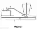
FIG. 1 shows an inventive arrangement.
DETAILED DESCRIPTION OF EMBODIMENTSFIG. 1 shows a support 1 with two insulating coatings, between which metallized surfaces and/or circuit board conductors 2 are arranged. A semiconductor chip 3 is arranged on one surface of the support 1. Through-plating 9, by means of which contact can be made with the metallized surface or circuit board conductor 2, passes through the support layer, on which the semiconductor chip 3 is arranged. According to the invention no contact pad is provided on the support surface but a first nail head contact 4 is applied, from which the wire has been separated. On a contact pad (not shown) of the semiconductor chip 3 a second nail head contact 5 is produced from which the wire 6 connecting the semiconductor chip 3 to the through-plating 9 runs to the first nail head contact 4 and is connected to this there by means of a wedge contact 7. In the example shown the first nail head contact 4 is pushed to some degree into the hole in the support layer of the through-plating 9 so that there is good contact with the metallization of the hole.
The invention is not restricted to use with multi-layer supports with intermediate metallization but can also be used on single-layer supports with metallized backs.
In FIG. 1 the capillary 8 of the bonding tool is also shown to clarify the inventive method.
Claims
1. An arrangement comprising: a semiconductor chip, and a support, said support having a contact point and a wire having first and second ends, said wire connecting a contact pad of the chip to said contact point, said contact point having a first nail head contact formed thereon, the first end of the wire connected to a second nail head contact with the contact pad of the chip, the second end of the wire connected via a wedge contact to the first nail head contact, wherein the contact point comprises a through-plating in the support and the first nail head contact is applied directly to the support surface at the site of the through-plating without further surface metallization.
2. An arrangement according to claim 1, wherein the support is formed using a ceramic material.
3. An arrangement according to claim 1, wherein the support is formed using a multi-layer ceramic material and the through-plating connects one surface of the support to metallization between two ceramic layers.
4. An arrangement according to claim 1, wherein the support is a PC board.
5. An arrangement according to claim 1, wherein the support is formed using a multi-layer PC board and the through-plating connects one surface of the support to metallization between two PC board layers.
6. A method for the electrical connection of a contact pad of a semiconductor chip to through-plating on a support, said method comprising the following steps:
forming a first nail head contact directly on the support surface at the site of the through-plating without further metallization using the capillary of a bonding tool,
separating the wire from the first nail head contact,
forming a second nail head contact on the contact pad of the semiconductor chip using the capillary of the bonding tool,
passing the wire to the first nail head contact, and
forming a wedge contact with the end of the wire on the first nail head contact using the capillary of the bonding tool.
Images & Drawings included:

Sources:
- United States Patent and Trademark Office - verify current appl. status at the USPTO↗
Recent applications in this class:
- » 20250266392 2025-08-21
Semiconductor packaging method and semiconductor packaging structure - » 20250239567 2025-07-24
METHODS OF FORMING WIRE INTERCONNECT STRUCTURES AND RELATED WIRE BONDING TOOLS - » 20250201765 2025-06-19
METHODS OF OPERATING WIRE BONDING SYSTEMS, INCLUDING METHODS OF DETECTING AND/OR PREVENTING WIRE FLY-OUT ON SUCH SYSTEMS - » 20250192098 2025-06-12
SEMICONDUCTOR APPARATUS AND METHOD FOR MANUFACTURING THE SAME, AND POWER CONVERSION APPARATUS - » 20250149502 2025-05-08
CAPILLARY FOR A WIRE BONDING MACHINE HAVING A DYNAMICALLY ADJUSTABLE CHAMFER DIAMETER - » 20250140740 2025-05-01
METHOD OF MANUFACTURING SEMICONDUCTOR DEVICE - » 20250140739 2025-05-01
LASER ENHANCED WIRE BONDING FOR SEMICONDUCTOR DEVICE PACKAGES - » 20250125305 2025-04-17
METHOD OF MANUFACTURING SEMICONDUCTOR DEVICE WITH FIXING FEATURE ON WHICH BONDING WIRE IS DISPOSED - » 20250118705 2025-04-10
PACKAGE-ON-PACKAGE ASSEMBLY WITH WIRE BOND VIAS - » 20250118704 2025-04-10
APPARATUS AND METHODS FOR TOOL MARK FREE STITCH BONDING
Recent applications for this Assignee:
- » 20250262772 2025-08-21
PLACE CONDITIONED PICK FOR ROBOTIC PICK AND PLACE OPERATIONS - » 20250242498 2025-07-31
SYSTEM AND METHOD FOR PICK POSE ESTIMATION FOR ROBOTIC PICKING WITH ARBITRARILY SIZED END EFFECTORS - » 20250216836 2025-07-03
PRIORITIZATION BETWEEN AGENTS IN AGENT-BASED PROCESS AUTOMATION - » 20250168873 2025-05-22
WLAN Communication Method and Devices - » 20250168152 2025-05-22
Communication System, Adapter for a Terminal and Method for Securely Transmitting Time-Critical Data within the Communication System - » 20250166165 2025-05-22
TRAINING SYSTEMS FOR SURFACE ANOMALY DETECTION - » 20250162095 2025-05-22
Method for Operating a Machine Tool, Computer Program Product, Control Unit, Machine Tool, Simulation Program Product and Use of the Control Unit - » 20250147755 2025-05-08
INDUSTRIAL APPLICATION PACKAGE MANAGEMENT - » 20250126041 2025-04-17
METHOD OF CAPTURING PACKETS FROM APPLICATIONS HOSTED ON CONTAINERS - » 20250117920 2025-04-10
SELF-SUPERVISED ANOMALY DETECTION FRAMEWORK FOR VISUAL QUALITY INSPECTION IN MANUFACTRUING