Semiconductor package
US20050189641A1
2005-09-01
11/115,236
2005-04-27
Abstract:
A semiconductor package comprises a first chip, a substrate, a middle layer, a second chip, and an encapsulant. The first chip has an active surface and a high-frequency element defining a high-frequency area on the active surface. The substrate supports the first chip and is electrically connected to the first chip. The middle layer is disposed on the first chip and has a recess corresponding to the high-frequency area. The second chip is disposed on the middle layer and electrically connected to either the first chip or the substrate. The encapsulant encapsulates the first chip, the middle layer, the second chip, and a part of the substrate.
Inventors:
- Chi-Tsung Chiu 38 🇹🇼 Kaohsiung, Taiwan
- Sung-Mao WU 9 🇹🇼 KAOHSIUNG, Taiwan
- Su Tao 15 🇹🇼 Kaohsiung, Taiwan
Assignee:
- ADVANCED SEMICONDUCTOR ENGINEERING, INC. 1,850 🇹🇼 Kaohsiung, Taiwan
Interested in similar patents?
Get notified when new applications in this technology area are published.
Classification:
H01L2924/15311 » CPC further
Indexing scheme for arrangements or methods for connecting or disconnecting semiconductor or solid-state bodies as covered by; Details of package parts other than the semiconductor or other solid state devices to be connected; Die mounting substrate; Connection portion the connection portion being formed only on the surface of the substrate opposite to the die mounting surface being a ball array, e.g. BGA
H01L2224/73204 » CPC further
Indexing scheme for arrangements for connecting or disconnecting semiconductor or solid-state bodies and methods related thereto as covered by; Means for bonding being of different types provided for in two or more of groups; Location after the connecting process on the same surface; Bump and layer connectors the bump connector being embedded into the layer connector
H01L23/66 » CPC main
Details of semiconductor or other solid state devices; Structural electrical arrangements for semiconductor devices not otherwise provided for, e.g. in combination with batteries; Impedance arrangements High-frequency adaptations
H01L21/563 » CPC further
Processes or apparatus adapted for the manufacture or treatment of semiconductor or solid state devices or of parts thereof; Manufacture or treatment of semiconductor devices or of parts thereof the devices having at least one potential-jump barrier or surface barrier, e.g. PN junction, depletion layer or carrier concentration layer; Assembly of semiconductor devices using processes or apparatus not provided for in a single one of the subgroups - , e.g. sealing of a cap to a base of a container; Encapsulations, e.g. encapsulation layers, coatings Encapsulation of active face of flip-chip device, e.g. underfilling or underencapsulation of flip-chip, encapsulation preform on chip or mounting substrate
H01L23/315 » CPC further
Details of semiconductor or other solid state devices; Encapsulations, e.g. encapsulating layers, coatings, e.g. for protection characterised by the arrangement or shape the device being completely enclosed the encapsulation having a cavity
H01L24/32 » CPC further
Arrangements for connecting or disconnecting semiconductor or solid-state bodies; Methods or apparatus related thereto; Means for bonding being attached to, or being formed on, the surface to be connected, e.g. chip-to-package, die-attach, "first-level" interconnects; Manufacturing methods related thereto; Layer connectors, e.g. plate connectors, solder or adhesive layers; Manufacturing methods related thereto; Structure, shape, material or disposition of the layer connectors after the connecting process of an individual layer connector
H01L24/83 » CPC further
Arrangements for connecting or disconnecting semiconductor or solid-state bodies; Methods or apparatus related thereto; Methods for connecting semiconductor or other solid state bodies using means for bonding being attached to, or being formed on, the surface to be connected using a layer connector
H01L25/0657 » CPC further
Assemblies consisting of a plurality of individual semiconductor or other solid state devices ; Multistep manufacturing processes thereof all the devices being of a type provided for in the same subgroup of groups - , e.g. assemblies of rectifier diodes the devices not having separate containers the devices being of a type provided for in group Stacked arrangements of devices
H01L23/3128 » CPC further
Details of semiconductor or other solid state devices; Encapsulations, e.g. encapsulating layers, coatings, e.g. for protection characterised by the arrangement or shape the device being completely enclosed a substrate forming part of the encapsulation the substrate having spherical bumps for external connection
H01L24/48 » CPC further
Arrangements for connecting or disconnecting semiconductor or solid-state bodies; Methods or apparatus related thereto; Means for bonding being attached to, or being formed on, the surface to be connected, e.g. chip-to-package, die-attach, "first-level" interconnects; Manufacturing methods related thereto; Wire connectors; Manufacturing methods related thereto; Structure, shape, material or disposition of the wire connectors after the connecting process of an individual wire connector
H01L24/73 » CPC further
Arrangements for connecting or disconnecting semiconductor or solid-state bodies; Methods or apparatus related thereto Means for bonding being of different types provided for in two or more of groups , , , , , , ,
H01L2224/73203 » CPC further
Indexing scheme for arrangements for connecting or disconnecting semiconductor or solid-state bodies and methods related thereto as covered by; Means for bonding being of different types provided for in two or more of groups; Location after the connecting process on the same surface Bump and layer connectors
H01L2224/8319 » CPC further
Indexing scheme for arrangements for connecting or disconnecting semiconductor or solid-state bodies and methods related thereto as covered by; Methods for connecting semiconductor or other solid state bodies using means for bonding being attached to, or being formed on, the surface to be connected using a layer connector Arrangement of the layer connectors prior to mounting
H01L2224/8385 » CPC further
Indexing scheme for arrangements for connecting or disconnecting semiconductor or solid-state bodies and methods related thereto as covered by; Methods for connecting semiconductor or other solid state bodies using means for bonding being attached to, or being formed on, the surface to be connected using a layer connector; Bonding techniques using a polymer adhesive, e.g. an adhesive based on silicone, epoxy, polyimide, polyester
H01L2225/06506 » CPC further
Details relating to assemblies covered by the group but not provided for in its subgroups; All the devices being of a type provided for in the same subgroup of groups - the devices not having separate containers the devices being of a type provided for in group; Stacked arrangements of devices Wire or wire-like electrical connections between devices
H01L2225/0651 » CPC further
Details relating to assemblies covered by the group but not provided for in its subgroups; All the devices being of a type provided for in the same subgroup of groups - the devices not having separate containers the devices being of a type provided for in group; Stacked arrangements of devices Wire or wire-like electrical connections from device to substrate
H01L2225/06568 » CPC further
Details relating to assemblies covered by the group but not provided for in its subgroups; All the devices being of a type provided for in the same subgroup of groups - the devices not having separate containers the devices being of a type provided for in group; Stacked arrangements of devices; Geometry of the stack, e.g. form of the devices, geometry to facilitate stacking the devices decreasing in size, e.g. pyramidical stack
H01L2924/01006 » CPC further
Indexing scheme for arrangements or methods for connecting or disconnecting semiconductor or solid-state bodies as covered by; Chemical elements Carbon [C]
H01L2924/01033 » CPC further
Indexing scheme for arrangements or methods for connecting or disconnecting semiconductor or solid-state bodies as covered by; Chemical elements Arsenic [As]
H01L2924/01082 » CPC further
Indexing scheme for arrangements or methods for connecting or disconnecting semiconductor or solid-state bodies as covered by; Chemical elements Lead [Pb]
H01L2924/01087 » CPC further
Indexing scheme for arrangements or methods for connecting or disconnecting semiconductor or solid-state bodies as covered by; Chemical elements Francium [Fr]
H01L2924/014 » CPC further
Indexing scheme for arrangements or methods for connecting or disconnecting semiconductor or solid-state bodies as covered by; Alloys Solder alloys
H01L2924/07802 » CPC further
Indexing scheme for arrangements or methods for connecting or disconnecting semiconductor or solid-state bodies as covered by; Polymers; Adhesive characteristics other than chemical not being an ohmic electrical conductor
H01L2924/19041 » CPC further
Indexing scheme for arrangements or methods for connecting or disconnecting semiconductor or solid-state bodies as covered by; Details of hybrid assemblies other than the semiconductor or other solid state devices to be connected; Structure; Component type being a capacitor
H01L2924/19042 » CPC further
Indexing scheme for arrangements or methods for connecting or disconnecting semiconductor or solid-state bodies as covered by; Details of hybrid assemblies other than the semiconductor or other solid state devices to be connected; Structure; Component type being an inductor
H01L2924/19043 » CPC further
Indexing scheme for arrangements or methods for connecting or disconnecting semiconductor or solid-state bodies as covered by; Details of hybrid assemblies other than the semiconductor or other solid state devices to be connected; Structure; Component type being a resistor
H01L2924/00 » CPC further
Indexing scheme for arrangements or methods for connecting or disconnecting semiconductor or solid-state bodies as covered by
H01L2924/181 » CPC further
Indexing scheme for arrangements or methods for connecting or disconnecting semiconductor or solid-state bodies as covered by; Details of package parts other than the semiconductor or other solid state devices to be connected Encapsulation
H01L2924/00012 » CPC further
Indexing scheme for arrangements or methods for connecting or disconnecting semiconductor or solid-state bodies as covered by; Technical content checked by a classifier Relevant to the scope of the group, the symbol of which is combined with the symbol of this group
H01L2224/85399 » CPC further
Indexing scheme for arrangements for connecting or disconnecting semiconductor or solid-state bodies and methods related thereto as covered by; Methods for connecting semiconductor or other solid state bodies using means for bonding being attached to, or being formed on, the surface to be connected using a wire connector; Bonding interfaces outside the semiconductor or solid-state body Material
H01L2224/05599 » CPC further
Indexing scheme for arrangements for connecting or disconnecting semiconductor or solid-state bodies and methods related thereto as covered by; Means for bonding being attached to, or being formed on, the surface to be connected, e.g. chip-to-package, die-attach, "first-level" interconnects; Manufacturing methods related thereto; Bonding areas; Manufacturing methods related thereto; Structure, shape, material or disposition of the bonding areas prior to the connecting process of an individual bonding area; External layer Material
H01L2924/0665 » CPC further
Indexing scheme for arrangements or methods for connecting or disconnecting semiconductor or solid-state bodies as covered by; Polymers Epoxy resin
H01L2224/45099 » CPC further
Indexing scheme for arrangements for connecting or disconnecting semiconductor or solid-state bodies and methods related thereto as covered by; Means for bonding being attached to, or being formed on, the surface to be connected, e.g. chip-to-package, die-attach, "first-level" interconnects; Manufacturing methods related thereto; Wire connectors; Manufacturing methods related thereto; Structure, shape, material or disposition of the wire connectors prior to the connecting process of an individual wire connector; Core members of the connector Material
H01L2924/00014 » CPC further
Indexing scheme for arrangements or methods for connecting or disconnecting semiconductor or solid-state bodies as covered by; Technical content checked by a classifier the subject-matter covered by the group, the symbol of which is combined with the symbol of this group, being disclosed without further technical details
H01L2924/207 » CPC further
Indexing scheme for arrangements or methods for connecting or disconnecting semiconductor or solid-state bodies as covered by; Parameters Diameter ranges
H01L2224/73265 » CPC further
Indexing scheme for arrangements for connecting or disconnecting semiconductor or solid-state bodies and methods related thereto as covered by; Means for bonding being of different types provided for in two or more of groups; Location after the connecting process on different surfaces Layer and wire connectors
Description
CROSS REFERENCE TO RELATED APPLICATIONThis application claims the priority benefit of Taiwan patent application serial No. 091135502, filed on Dec. 3, 2002, and the full disclosure thereof is incorporated herein by reference.
BACKGROUND OF THE INVENTION1. Field of the Invention
The present invention relates to a semiconductor package with a high-frequency element, and more particularly, to a semiconductor package with a cavity formed in the encapsulant corresponding to a high-frequency element thereof so as to avoid the influence of the encapsulant upon the high-frequency element.
2. Description of the Related Art
The package has four major functions, i.e. signal distribution, power distribution, heat dissipation, and protection. In general, the semiconductor chip is formed into an enclosure, such as a single-chip module (SCM) or a chip carrier, referred to as a first-level package, i.e. the packaging of the semiconductor. These packaged chips, along with other components such as capacitors, resistors, inductors, filters, switches, and optical and RF components, are assembled to a printed wiring board in a second-level package.
In the prior art, there exist varied packages, such as a small outline package (SOP), a quad flat package (QFP), a ball grid array (BGA) package, and so on.
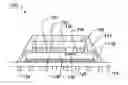
Referring to FIG. 1, it depicts a typical ball grid array package 10. The package 10 generally has a substrate 14 and a chip 18 attached on the substrate 14 by an adhesive 28. The chip 18 is electrically connected to the substrate 14 through a plurality of bonding wires 16. An encapsulant 12 encapsulates the substrate 14, the chip 18, and the bonding wires 16. The substrate 14 further has a plurality of solder balls 24 for electrically connecting an external circuit.
The active surface 26 of the chip 18 typically directly touches the encapsulant 12. However, in a specific case, the chip 18 is provided with a high-frequency circuit or element disposed in a high-frequency area 20 on the active surface 26. The signal propagation speed Vp in the high-frequency element is derived from the following equation:
Vp=C/{square root}{square root over ( )}(εr)
where C is the speed of light in vacuum and εr is effective or equivalent dielectric constant. As the high-frequency element is exposed to air, the effective dielectric constant ranges from 1 (the dielectric constant of air) to 4 (the dielectric constant of G-10 or FR-4 substrate which is constructed from a woven glass fabric with an epoxy resin binder). However, while the high-frequency area 20 is covered with the encapsulant 12, the dielectric constant of the encapsulant 12 is larger than that of the air and thus the effective dielectric constant ranges from the dielectric constant of the encapsulant 12 to the dielectric constant of the substrate 14. Therefore, the effective dielectric constant of the substrate covered with the encapsulant 12 is larger than that of the substrate exposed to the air. Furthermore, the loss factor or loss tangent of the high-frequency circuit is also increased because of the covering of the encapsulant 12.
Accordingly, there exists a need for a semiconductor package which is provide with a cavity to prevent the high-frequency element from contacting the encapsulant and avoid the disadvantages due to the contact.
SUMMARY OF THE INVENTIONIt is an object of the present invention to provide a semiconductor package with a cavity positioned above the high-frequency area of the semiconductor chip such that the propagation speed of the high-frequency circuit is not reduced.
In order to achieve the above object, the present invention provides a semiconductor package comprising a first chip, a substrate, a middle layer, a second chip, and an encapsulant. The first chip has an active surface and a high-frequency element defining a high-frequency area on the active surface. The substrate supports the first chip and is electrically connected to the first chip. The middle layer is disposed on the first chip and has a recess corresponding to the high-frequency area. The second chip is disposed on the middle layer and electrically connected to either the first chip or the substrate. The encapsulant encapsulates the first chip, the middle layer, the second chip, and a part of the substrate.
Accordingly, the high-frequency element of the semiconductor package according to the present invention is not covered with or touched by the encapsulant, and thus the propagation speed of the high-frequency element may not be reduced by the influence of the encapsulant. Furthermore, the high-frequency element is not covered with the encapsulant and thus the loss tangent thereof is not increased.
BRIEF DESCRIPTION OF THE DRAWINGSOther objects, advantages, and novel features of the invention will become more apparent from the following detailed description when taken in conjunction with the accompanying drawing.
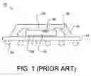
FIG. 1 is a schematic cross-sectional view of a semiconductor package in the prior art.
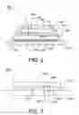
FIG. 2 is a schematic cross-sectional view of a semiconductor package according to an embodiment of the present invention.
FIG. 3 is a schematic cross-sectional view of a semiconductor package according to another embodiment of the present invention.
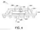
FIG. 4 is a schematic cross-sectional view of a semiconductor package according to a further embodiment of the present invention.
DESCRIPTION OF THE PREFERRED EMBODIMENTReferring to FIG. 2, it depicts a semiconductor package 100 according to an embodiment of the present invention. The semiconductor package 100 is a multi-chip package and has a first chip 118 attached to a substrate 114 by an adhesive 128, and a second chip 130 disposed on the first chip 118.
The first chip 118 has an active surface 126 electrically connected to the substrate 114 by a plurality of bonding wires 116. The substrate 114 further has a plurality of solder balls 124 for connecting an external circuit. The first chip 118 has high-frequency circuits or elements disposed in a high-frequency area 120 on the active surface 126 of the first chip 118.
A middle layer 132 is disposed on the active surface 126 of the first chip 118 and has a recess 134 corresponding to the high-frequency area 120. The middle layer 132 can be an adhesive, such as made of epoxy, and be applied on the active surface 126 by screen-printing, thereby forming the recess 134. The second chip 130 is disposed on the middle layer 132 and electrically connected to the first chip by a plurality of bonding wires 136. An encapsulant 112 encapsulates the substrate 114, the first chip 118, the middle layer 132, the second chip 130, and the bonding wires 116 and 136.
In this arrangement, the high-frequency area 120 of the first chip 118 is exposed to the recess 134, so the propagation speed of the high-frequency element in the high-frequency area 120 is free from the influence of the encapsulant 112 and thus is not reduced. Furthermore, without being covered by the encapsulant 112, the loss tangent of the high-frequency element is not increased. It should be noticed that the recess 134 shown in the drawing is a through hole, but the recess 134 is used for providing a space above the high-frequency area and can be a non-through hole, i.e. a depression.
Referring to FIG. 3, it depicts a semiconductor package 200 according to another embodiment of the present invention. The semiconductor package 200 is a type of flip chip package and has a chip 218 having an active surface 226 which is electrically connected to a substrate 214 by bumps 216. An encapsulant 212 is filled between the active surface 226 of the chip 218 and the substrate 214 by the underfill dispensing process. The substrate 214 is adapted for electrically connecting an external circuit.
The chip 218 has a high-frequency circuit or element disposed in a high-frequency area 220 on the active surface 126 of the first chip 118. As shown in the drawing, the active surface 226 of the chip 218 faces the substrate 214. The encapsulant 212 has a cavity 234 (a through hole shown in the drawing), the position of which is corresponding to that of the high-frequency area 220. In this arrangement, the high-frequency area 220 is exposed to the cavity 234, so the propagation speed of the high-frequency element in the high-frequency area 220 is free from the influence of the encapsulant 212 and is not reduced.
It will be apparent to those skilled in the art that the cavity 234 or the through hole can be formed by dispensing and performing a dam (not shown).
Furthermore, the substrate 214 can be provided with a notch 236 disposed thereon corresponding to the high-frequency area 220 for increasing the volume of the space above the high-frequency area 220 and further reducing the influence upon the high-frequency area.
Referring to FIG. 4, it depicts a semiconductor package 300 according to a further embodiment of the present invention. The semiconductor package 300 has a chip 318 which is attached to the substrate 214 by an adhesive layer 328. The chip 318 has an active surface 326 which is electrically connected to the substrate 314 by a plurality of bonding wires 316. The substrate 14 is further provided with a plurality of solder balls 324 for connecting an external circuit.
The chip 318 has a high-frequency circuit or element disposed in a high-frequency area 320 on the active surface 326 of the chip 318. An encapsulant 312 encapsulates the substrate 314, the chip 318, and the bonding wires 316. As shown in the drawing, the encapsulant 312 has a cavity 334 corresponding to the high-frequency area 320. It will be apparent to those skilled in the art that the cavity 334 can be formed in the encapsulant 312 by pre-locating a lip (not shown) thereon and then molding the encapsulant 312.
It will be apparent to those skilled in the art that the principle and spirit of the present invention is that a space positioned above the high-frequency element of a semiconductor chip is provided such that the influence upon the operation of the high-frequency element is avoided. The principle of the present invention is not limited to be applied to the embodiments shown in the drawings and can be applied to other packages, such as small outline packages, quad flat packages, ball grid array packages and so on. The above-mentioned substrate can be easily replaced with a lead frame.
As mentioned above, the high-frequency element of the semiconductor package according to the present invention is not covered with or touched by the encapsulant, and thus the propagation speed of the high-frequency element may not be reduced by the influence of the encapsulant. Furthermore, the high-frequency element is not covered with the encapsulant and thus the loss tangent thereof is not increased.
While the foregoing description and drawings represent the preferred embodiments of the present invention, it will be understood that various additions, modifications and substitutions may be made therein without departing from the spirit and scope of the principles of the present invention as defined in the accompanying claims. One skilled in the art will appreciate that the invention may be used with many modifications of form, structure, arrangement, proportions, materials, elements, and components and otherwise, used in the practice of the invention, which are particularly adapted to specific environments and operative requirements without departing from the principles of the present invention. The presently disclosed embodiments are therefore to be considered in all respects as illustrative and not restrictive, the scope of the invention being indicated by the appended claims and their legal equivalents, and not limited to the foregoing description.
Claims
1-11. (canceled)
12. A semiconductor package comprising:
a chip defining an active surface and having a high-frequency element defining a high-frequency area on the active surface;
a substrate supporting the chip and electrically connected to the chip;
an encapsulant encapsulating the active surface of the chip, and a part of the substrate; and
a cavity positioned within the encapsulant above the high-frequency area.
13. The semiconductor package as claimed in claim 12, wherein the substrate further has a plurality of solder balls for electrically connecting an external circuit.
14. The semiconductor package as claimed in claim 12, further comprising:
a plurality of bonding wires for electrically connecting the chip to the substrate.
Images & Drawings included:
Sources:
- United States Patent and Trademark Office - verify current appl. status at the USPTO↗
Similar patent applications:
- » 20230207416
Semiconductor devices including a lower semiconductor package, an upper semiconductor package on the lower semiconductor package, and a connection pattern between the lower semiconductor package and the upper semiconductor package - » 20210343617
Semiconductor devices including a lower semiconductor package, an upper semiconductor package on the lower semiconductor package, and a connection pattern between the lower semiconductor package and the upper semiconductor package - » 20110079890
Semiconductor package, semiconductor package structure including the semiconductor package, and mobile phone including the semiconductor package structure - » 20250149527
SEMICONDUCTOR PACKAGE, SEMICONDUCTOR PACKAGE INTERMEDIATE, REDISTRIBUTION LAYER CHIP, REDISTRIBUTION LAYER CHIP INTERMEDIATE, METHOD OF MANUFACTURING SEMICONDUCTOR PACKAGE, AND METHOD OF MANUFACTURING SEMICONDUCTOR PACKAGE INTERMEDIATE - » 20120064666
MANUFACTURING METHOD OF SUBSTRATE FOR A SEMICONDUCTOR PACKAGE, MANUFACTURING METHOD OF SEMICONDUCTOR PACKAGE, SUBSTRATE FOR A SEMICONDUCTOR PACKAGE AND SEMICONDUCTOR PACKAGE - » 20130309818
Manufacturing method of substrate for a semiconductor package, manufacturing method of semiconductor package, substrate for a semiconductor package and semiconductor package - » 20100213620
Manufacturing method of substrate for a semiconductor package, manufacturing method of semiconductor package, substrate for a semiconductor package and semiconductor package - » 20190267315
Method of manufacturing semiconductor package substrate and semiconductor package substrate manufactured using the method, and method of manufacturing semiconductor package and semiconductor package manufactured using the method - » 20080157394
Semiconductor packages, stacked semiconductor packages, and methods of manufacturing the semiconductor packages and the stacked semiconductor packages - » 20110014748
Semiconductor packages, stacked semiconductor packages, and methods of manufacturing the semiconductor packages and the stacked semiconductor packages
Recent applications in this class:
- » 20250174583 2025-05-29
HIGH FREQUENCY MODULE AND COMMUNICATION DEVICE - » 20250174582 2025-05-29
ELECTRONIC PACKAGE AND MANUFACTURING METHOD THEREOF - » 20250167143 2025-05-22
POWER AMPLIFIER DIE - » 20250167142 2025-05-22
PITCH-REDUCING SOLDER INTERCONNECT FOR RF TRANSITIONS - » 20250157954 2025-05-15
METHOD OF FABRICATING RADIO-FREQUENCY MULTI-LAYER CIRCUITS ON FUSED SILICA - » 20250157953 2025-05-15
VERTICAL SEMICONDUCTOR RFID STRUCTURE, RFID TAG DEVICE, AND MANUFACTURING METHOD THEREOF - » 20250149473 2025-05-08
RF ABSORBING COVER INTEGRATED IN MMIC PACKAGES - » 20250149472 2025-05-08
HIGH-FREQUENCY CIRCUIT COMPONENT - » 20250140717 2025-05-01
STRIPLINE MONOLITHIC MICROWAVE INTEGRATED CIRCUIT (MMIC) INTERCONNECT ON RECESSED LOW TEMPERATURE CO-FIRED CERAMIC (LTCC) - » 20250132273 2025-04-24
ELECTRONIC PACKAGE INCLUDING LEAD FRAME HAVING MULTIPLE CONDUCTIVE POSTS
Recent applications for this Assignee:
- » 20250174898 2025-05-29
ANTENNA DEVICE - » 20250174536 2025-05-29
ELECTRONIC PACKAGE STRUCTURE - » 20250174508 2025-05-29
SEMICONDUCTOR DEVICE PACKAGE - » 20250167440 2025-05-22
SEMICONDUCTOR DEVICE PACKAGE AND METHOD OF MANUFACTURING THE SAME - » 20250167131 2025-05-22
OPTICAL PACKAGE STRUCTURE - » 20250167092 2025-05-22
ELECTRONIC DEVICE - » 20250159793 2025-05-15
ELECTRONIC DEVICE - » 20250157972 2025-05-15
ELECTRONIC PACKAGE STRUCTURE AND METHOD FOR MANUFACTURING THE SAME - » 20250157947 2025-05-15
WIRING STRUCTURE AND METHOD FOR MANUFACTURING THE SAME - » 20250157888 2025-05-15
ELECTRONIC DEVICE