Bonding pad arrangement method for semiconductor devices
US20050194664A1
2005-09-08
11/107,897
2005-04-18
Abstract:
A variety of pad arrangements are provided for semiconductor devices for reducing the likelihood of bonding failures, particularly those due to shorts, and/or for reducing the difference in length between bonding wires to decrease signal skew during operation of the semiconductor device and improve signal integrity.
Inventors:
- Ho-Cheol Lee 1 🇰🇷 Yongin-shi, South Korea
- Jae-Hoon Kim 1 🇰🇷 Suwon-shi, South Korea
- Jung-Su Ryu 1 🇰🇷 Seongnam-shi, South Korea
Interested in similar patents?
Get notified when new applications in this technology area are published.
Classification:
H01L2924/00014 » CPC further
Indexing scheme for arrangements or methods for connecting or disconnecting semiconductor or solid-state bodies as covered by; Technical content checked by a classifier the subject-matter covered by the group, the symbol of which is combined with the symbol of this group, being disclosed without further technical details
H01L24/06 » CPC main
Arrangements for connecting or disconnecting semiconductor or solid-state bodies; Methods or apparatus related thereto; Means for bonding being attached to, or being formed on, the surface to be connected, e.g. chip-to-package, die-attach, "first-level" interconnects; Manufacturing methods related thereto; Bonding areas ; Manufacturing methods related thereto; Structure, shape, material or disposition of the bonding areas prior to the connecting process of a plurality of bonding areas
H01L23/50 » CPC further
Details of semiconductor or other solid state devices; Arrangements for conducting electric current to or from the solid state body in operation, e.g. leads, terminal arrangements ; Selection of materials therefor for integrated circuit devices, e.g. power bus, number of leads
H01L24/48 » CPC further
Arrangements for connecting or disconnecting semiconductor or solid-state bodies; Methods or apparatus related thereto; Means for bonding being attached to, or being formed on, the surface to be connected, e.g. chip-to-package, die-attach, "first-level" interconnects; Manufacturing methods related thereto; Wire connectors; Manufacturing methods related thereto; Structure, shape, material or disposition of the wire connectors after the connecting process of an individual wire connector
H01L24/49 » CPC further
Arrangements for connecting or disconnecting semiconductor or solid-state bodies; Methods or apparatus related thereto; Means for bonding being attached to, or being formed on, the surface to be connected, e.g. chip-to-package, die-attach, "first-level" interconnects; Manufacturing methods related thereto; Wire connectors; Manufacturing methods related thereto; Structure, shape, material or disposition of the wire connectors after the connecting process of a plurality of wire connectors
H01L2224/04042 » CPC further
Indexing scheme for arrangements for connecting or disconnecting semiconductor or solid-state bodies and methods related thereto as covered by; Means for bonding being attached to, or being formed on, the surface to be connected, e.g. chip-to-package, die-attach, "first-level" interconnects; Manufacturing methods related thereto; Bonding areas; Manufacturing methods related thereto; Structure, shape, material or disposition of the bonding areas prior to the connecting process Bonding areas specifically adapted for wire connectors, e.g. wirebond pads
H01L2224/4912 » CPC further
Indexing scheme for arrangements for connecting or disconnecting semiconductor or solid-state bodies and methods related thereto as covered by; Means for bonding being attached to, or being formed on, the surface to be connected, e.g. chip-to-package, die-attach, "first-level" interconnects; Manufacturing methods related thereto; Wire connectors; Manufacturing methods related thereto; Structure, shape, material or disposition of the wire connectors after the connecting process of a plurality of wire connectors; Disposition Layout
H01L2924/01006 » CPC further
Indexing scheme for arrangements or methods for connecting or disconnecting semiconductor or solid-state bodies as covered by; Chemical elements Carbon [C]
H01L2924/01023 » CPC further
Indexing scheme for arrangements or methods for connecting or disconnecting semiconductor or solid-state bodies as covered by; Chemical elements Vanadium [V]
Y10T29/49121 » CPC further
Metal working; Method of mechanical manufacture; Electrical device making; Conductor or circuit manufacturing Beam lead frame or beam lead device
H01L2224/45099 » CPC further
Indexing scheme for arrangements for connecting or disconnecting semiconductor or solid-state bodies and methods related thereto as covered by; Means for bonding being attached to, or being formed on, the surface to be connected, e.g. chip-to-package, die-attach, "first-level" interconnects; Manufacturing methods related thereto; Wire connectors; Manufacturing methods related thereto; Structure, shape, material or disposition of the wire connectors prior to the connecting process of an individual wire connector; Core members of the connector Material
H01L2224/05599 » CPC further
Indexing scheme for arrangements for connecting or disconnecting semiconductor or solid-state bodies and methods related thereto as covered by; Means for bonding being attached to, or being formed on, the surface to be connected, e.g. chip-to-package, die-attach, "first-level" interconnects; Manufacturing methods related thereto; Bonding areas; Manufacturing methods related thereto; Structure, shape, material or disposition of the bonding areas prior to the connecting process of an individual bonding area; External layer Material
H01L2224/85399 » CPC further
Indexing scheme for arrangements for connecting or disconnecting semiconductor or solid-state bodies and methods related thereto as covered by; Methods for connecting semiconductor or other solid state bodies using means for bonding being attached to, or being formed on, the surface to be connected using a wire connector; Bonding interfaces outside the semiconductor or solid-state body Material
H01L2924/00 » CPC further
Indexing scheme for arrangements or methods for connecting or disconnecting semiconductor or solid-state bodies as covered by
Description
This is a divisional application of U.S. patent application Ser. No. 10/465,554, filed on Jun. 20, 2003, which claims priority under 35 U.S.C. § 119 of Korean Patent Application 2002-35925 filed on Jun. 26, 2002, the entire contents of which are hereby incorporated by reference.
BACKGROUND OF THE INVENTION1. Field of the Invention
The present invention relates to a semiconductor device and, more particularly, to pad arrangements for reducing bonding failures and signal skew.
2. Discussion of the Related Art
As semiconductor manufacturing processes have improved, design rules have been reduced to allow for smaller and/or higher density semiconductor devices. However, for semiconductor devices having a large number of pads, the pad pitch limit, or pad-to-pad design rule, may define the minimum size.
FIGS. 1A to 1C are views of representative pad arrangements that are used on conventional semiconductor devices. FIG. 1A illustrates pads 98 arranged in a single row on a chip 100, FIG. 1B illustrates pads 98 arranged in two rows on a chip 100 and FIG. 1C illustrates pads 98 arranged around the periphery of a chip 100.
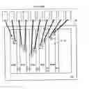
FIG. 2 illustrates a conventional configuration of bonding wires 104 used to connect two rows of bond pads to the corresponding portions of a lead frame 102. As reflected in FIG. 2, the separation between the bonding wires 104 used to connect pads 1-3, 6-11 and 14-16 to the corresponding portions of the lead frame 102 is reduced, increasing the likelihood that one or more shorts may be formed between a bond wire and a pad and/or an adjacent bond wire. Increasing the number of bond pads tends to reduce the spacing between adjacent bond wires and to increase the likelihood of shorts.
Further, bonding wires 104 connected between the more distant portions of the lead frame 102 and certain of the pads, e.g., pads 1, 8, 9 and 16, are substantially longer than those bonding wires connected between closer portions of the lead frame and other pads, e.g., pads 4, 5, 12 and 13. Different bonding wire lengths may result in a timing skew between the signals being transmitted through the bonding wires to the respective pads. These timing skews will tend to compromise signal integrity, disrupt high-speed operations and limit the rate at which the semiconductor device may be successfully operated.
SUMMARY OF THE INVENTIONAccordingly, exemplary embodiments of the invention are directed to a method of arranging pads on a semiconductor device in a manner that will tend to reduce the likelihood of shorts and/or reduce the signal time skew during operation of the semiconductor device.
Exemplary embodiments of the invention are directed to methods of arranging pads on semiconductor devices to allow a plurality of bonding wires to have substantially the same length.
Exemplary embodiments of the invention provide methods of arranging pads, such as pad-on-cell (POC) type pads, on semiconductor devices to form pad groupings having an oblique arrangement with respect to the chip edge and/or other pad groupings. Exemplary pad groupings configurations may be symmetrical or asymmetrical with respect to the chip edge and may include one or more V-shaped, sawtooth or zigzag-type pad arrangements that may allow reductions in the semiconductor package size, reduce the length variation in the bond wires, and reduce the likelihood of shorting between bonding wires and/or pads.
It is to be understood that both the foregoing general description and the following detailed description of the present invention are exemplary and explanatory and are intended to provide further explanation to those of skill in the art of the invention as claimed.
BRIEF DESCRIPTION OF THE DRAWINGSExemplary embodiments of the invention may be further understood through the written description and the accompanying FIGURES in which:
FIGS. 1A to 1C are plan views illustrating certain conventional pad arrangements;
FIG. 2 is a view illustrating a bonding wire configuration between a conventional lead from and semiconductor device pads with an increased likelihood of shorting or bonding failures;
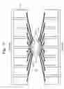
FIG. 3 is a plan view showing a pad arrangement in which lead frames are bonded with pads in accordance with a first exemplary embodiment of the invention;
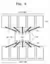
FIG. 4 is a plan view showing a pad arrangement in which lead frames are bonded with pads in accordance with a second exemplary embodiment of the invention;
FIG. 5 is a plan view of a pad arrangement in accordance with a third exemplary embodiment of the invention;
FIGS. 6A and 6B are plan views of pad arrangements in accordance with a fourth exemplary embodiment of the invention;
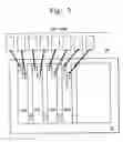
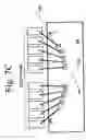
FIG. 7A is a plan view of a pad arrangement in accordance with a fifth exemplary embodiment of the invention, FIG. 7B is a plan view of a pad arrangement in which the angles α and β are substantially equal, FIG. 7C is a plan view of a pad arrangement in which the bonding wire have substantially equal lengths;
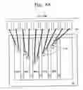
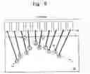
FIG. 8 is a plan view of a pad arrangement in accordance with a sixth exemplary embodiment of the invention;
FIG. 9 is a plan view of a pad arrangement in accordance with a seventh exemplary embodiment of the present invention; and FIG. 10 is a plan view of an embodiment in which two series of pads are arranged with the corresponding axes being substantially parallel.
DETAILED DESCRIPTION OF THE INVENTIONExemplary embodiments of the invention will be described below with reference to accompanying drawings. This invention may, however, be embodied in many different forms and should not be construed as being limited to the exemplary embodiments set forth herein; rather, these exemplary embodiments are provided so that this disclosure is thorough and complete, and conveys the concept of the invention to those skilled in the art. In the drawings, the sizing and spacing of elements may be enlarged or reduced for clarity and are not intended to be to scale.
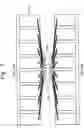
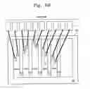
FIG. 3 is a plan view showing an arrangement of pads 1-16 on a semiconductor chip 100 according to a first exemplary embodiment of the invention with portions of a conventional lead frame 102 being connected to the pads with bonding wires 104. As illustrated in FIG. 3, pads 1-8 and 9-12 are arranged to form two shallow “V” shapes having legs arranged obliquely with respect to one of the edges 106 of chip 100.
As illustrated in FIG. 3, this arrangement of the pads allows the bonding wires 104 between the several end pads on each leg of the “V” shape, i.e., pads 1-3, 6-8, 9-11 and 14-16 to be bonded to a conventional lead frame 102 while improving the separation between adjacent bonding wires and the overlap of other pads to reduce the likelihood of shorting. Increasing the oblique angle between a group of pads and the edge of the chip can increase the number of pads that may be successfully bonded to the lead frame and permit the mounting of semiconductor devices having an increased number of pads.
FIG. 4 is a plan view showing an arrangement of pads 1-10 on a semiconductor chip 100 according to a second exemplary embodiment of the invention with portions of a conventional lead frame 102 being connected to the pads with bonding wires 104. As illustrated in FIG. 4, pads 1-5 and 6-10 are arranged in opposing “V” shapes configured to allow connection to a conventional lead frame 102 using bonding wires 104 of substantially equal length. By allowing the use of bonding wires of substantially equal length, this pad arrangement reduces signal skew and improves signal integrity.
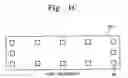
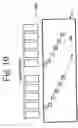
FIG. 5 is a plan view of a pad arrangement in accordance with a third exemplary embodiment of the invention. As illustrated in FIG. 5, a plurality of memory cell array blocks, including memory cell array blocks MCB0 to MCB3, and sense amplifiers, including S/A0 to S/A3, are provided on a semiconductor chip 100. Each of the memory cell array blocks is associated with a pair of pads, including pads 1-10, which may be POC-type pads. The pads in each memory cell array block are offset in such a manner that the first pads in each of the memory cell array blocks are arranged in a first line and the second pads in each of the memory cell array blocks are arranged in a second line, the first and second lines being substantially parallel to each other and to the edge 106 of the chip 100. The offset between the pads and the step distance between adjacent memory cell array blocks may be such that a line from a first pad to a second pad to the next first pad, e.g., from pad 1 to pad 2 to pad 3, etc., will have a somewhat zigzag or sawtooth pattern. Offsetting the pads in each of the memory cell array blocks in this manner increases the number of pads that can be successfully bonded to a lead frame when compared with pads arranged in a single row.
FIGS. 6A and 6B are plan views of pad arrangements in accordance with a fourth exemplary embodiment of the present invention. As illustrated in FIG. 6A, pads 1-10, which may be POC-type pads, are arranged on a semiconductor chip 100 over a plurality of memory cell array blocks, MCB0 to MCB4, in a general “V” shape with the point of the “V” directed toward the center of the chip. As did the pad arrangement illustrated in FIG. 4, the V-shaped pad arrangement illustrated in FIG. 6A allows the lengths of the bonding wires 104 used to connect the pads 98 and a lead frame (not shown) to be substantially equal, reducing the incidence of signal skew and improving the signal integrity.
As illustrated in FIG. 6B, the pads may also be arranged in a “V” shape in which the point of the “V” is directed away from the center toward the edge 106 of the chip 100. As it did in the exemplary embodiment illustrated in FIG. 3, this pad arrangement improves the separation between adjacent bonding wires, particularly for those pads at the ends of the legs of the “V,” and will reduce the likelihood of shorting.
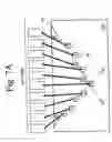
FIG. 7 is a plan view of a pad arrangement in accordance with a fifth exemplary embodiment of the present invention. As illustrated in FIG. 7, pads 1-10 are again arranged to form a somewhat asymmetric “V” shape. Pads 1-5 are generally aligned along a first line 108 defining a first oblique angle a with the edge 106 of chip 100. Similarly, pads 6-10 are generally aligned along a second line 110 defining a second oblique angle β with the edge 106 of chip 100. The selection of different angles α and β allows the pad arrangement to be adjusted to compensate for the off-center mounting of the chip 100 within a lead frame (not shown). In off-center mounting configurations, such as may be used in a multi-chip package, the selection of the angles α and β chips can improve the bonding performance by providing a larger effective angle for pads that are to be bonded to more distant portions of the lead frame while providing an angle that will tend to equalize the lengths of the bonding wires to pads that will be connected to closer portions of the lead frame.
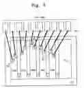
FIG. 8 is a plan view of a pad arrangement in accordance with a sixth exemplary embodiment of the present invention. As illustrated in FIG. 8, pads 1 to 10 are arranged over memory cell array blocks MCB0 to MCB4 in an asymmetric “V” shape with pads 1-5 forming a first leg of the “V” and pads 6-10 forming the second leg. Like the pad arrangement illustrated in FIG. 7, the oblique angle α formed between a line 108 though pads 1 to 5 and the edge 106 of chip 100 is different than the angle β formed between a line 110 through pads 6-10 and the edge 106 of chip 100.
FIG. 9 is a plan view of a pad arrangement in accordance with a seventh exemplary embodiment of the present invention. The pad arrangement illustrated in FIG. 9 is substantially similar to the pad arrangement illustrated in FIG. 8, except that the pads of FIG. 9 are conventional pads arranged on a semiconductor substrate rather than POC-type pads. The reasons for and the benefits resulting from such a pad arrangement are similar to those discussed in connection with FIG. 8.
Pad arrangements in accord with the exemplary embodiments of the invention make it possible to reduce the occurrence of shorts between the bonding wires, the pads and/or the lead frame in a semiconductor package. Pad arrangements in accord with the exemplary embodiments of the invention may also make it possible to reduce the difference in the length of the bonding wires, thereby reducing signal skew and improving signal integrity.
It will be apparent to those skilled in the art that various modifications and variations can be made in the present invention. Thus, it is intended that the present invention covers the modifications and variations of this invention provided they come within the scope of the appended claims and their equivalents.
Claims
1. A semiconductor device having a plurality of bond pads comprising:
a plurality of bond pad pairs, each pair of bond pads including a first bond pad and a second bond pad, wherein
each of the first bond pads is positioned at a first perpendicular distance from a first edge of the semiconductor device; and
each of the second bond pads is positioned at a second perpendicular distance from the first edge of the semiconductor device and separated from a corresponding first bond pad by a third distance in a direction parallel to the first edge of the semiconductor device, wherein:
the first and second perpendicular distances are not identical.
2. The semiconductor device according to claim 1, wherein:
the semiconductor device is configured as a pad-on-cell (POC) device including a plurality of memory cell array blocks, and wherein
at least one bond pad pair is arranged on each memory cell array block.
3. The semiconductor device according to claim 2, wherein:
each second bond pad is separated from an adjacent non-paired first bond pad by a step distance in a direction generally parallel to the first edge of the semiconductor device.
4. The semiconductor device according to claim 3, wherein:
the third distance is an offset distance.
5. The semiconductor device according to claim 3, wherein:
the offset distance and the step distance are approximately equal.
6. The semiconductor device according to claim 3, wherein:
a ratio between the offset distance and the step distance is at least 1:4.
7. A semiconductor package comprising:
a semiconductor device according to claim 1;
a lead frame, the lead frame including a plurality of connection regions, the connection regions being arranged along an axis substantially parallel to the first edge of the semiconductor device; and
a plurality of bond wires extending between connection regions of the lead frame and the bond pads, wherein:
the semiconductor device is configured as a pad-on-cell (POC) device that includes a plurality of memory cell array blocks, and further wherein, at least one bond pad pair is arranged over each memory cell array block.
8. A semiconductor package according to claim 7, wherein:
the semiconductor device includes
a second edge parallel to the first edge;
third and fourth edges perpendicular to the first and second edges; and
a plurality of third bond pads arranged adjacent at least one of the second, third and fourth edges of the semiconductor device.
9. The semiconductor package comprising:
a semiconductor device according to claim 1, wherein the semiconductor device is configured as a pad-on-cell (POC) device that includes a plurality of memory cell array blocks separated by a plurality of sense amplifiers and wherein adjacent ones of the bond pads are arranged over at least one memory cell array block.
10. The semiconductor package according to claim 9, wherein:
the bond pad pairs are positioned outside a periphery of the sense amplifiers.
11. The semiconductor package according to claim 9, wherein:
the semiconductor device includes
a second edge parallel to the first edge;
third and fourth edges perpendicular to the first and second edges; and
a plurality of third bond pads arranged adjacent at least one of the second, third and fourth edges of the semiconductor device.
Images & Drawings included:

Sources:
- United States Patent and Trademark Office - verify current appl. status at the USPTO↗
Recent applications in this class:
- » 20250174585 2025-05-29
SEMICONDUCTOR DIE AND SEMICONDUCTOR PACKAGE INCLUDING THE SAME - » 20250167149 2025-05-22
MANUFACTURING METHOD OF SEMICONDUCTOR STRUCTURE - » 20250157962 2025-05-15
SEMICONDUCTOR PACKAGE INCLUDING DUMMY PADS AND MANUFACTURING METHOD FOR THE SAME - » 20250149481 2025-05-08
SEMICONDUCTOR PACKAGE - » 20250149480 2025-05-08
SEMICONDUCTOR PACKAGE - » 20250149479 2025-05-08
SEMICONDUCTOR PACKAGE - » 20250149478 2025-05-08
SEMICONDUCTOR PACKAGE - » 20250149477 2025-05-08
PHOTONIC ASSEMBLY FOR ENHANCED BONDING YIELD AND METHODS FOR FORMING THE SAME - » 20250140723 2025-05-01
SEMICONDUCTOR PACKAGE AND METHOD OF MANUFACTURING A SEMICONDUCTOR PACKAGE - » 20250118692 2025-04-10
Mitigating process problems in hybrid bonding of vertical die stacking