Semiconductor device and circuit board
US20060284315A1
2006-12-21
11/455,172
2006-06-19
Abstract:
A semiconductor device 1 includes a silicon substrate 5, a semiconductor chip 2 placed on a surface S1 of the silicon substrate 5, a protruding electrode 6 (first protruding electrode) provided on a surface S2 of the semiconductor chip 2 opposite to the silicon substrate 5, and another protruding electrode 7 (second protruding electrode) provided on the surface S1 of the silicon substrate 5. Top portions of the protruding electrodes 6, 7 are of a generally same height from the surface S1 of the silicon substrate 5. In other words, the top portions of the protruding electrodes 6, 7 are flush on a plane parallel to the surface S1 of the silicon substrate 5.
Assignee:
- NEC ELECTRONICS CORPORATION 1,493 🇯🇵 Kanagawa, Japan
Interested in similar patents?
Get notified when new applications in this technology area are published.
Classification:
H01L23/147 » CPC main
Details of semiconductor or other solid state devices; Mountings, e.g. non-detachable insulating substrates characterised by the material or its electrical properties Semiconductor insulating substrates
H01L23/49805 » CPC further
Details of semiconductor or other solid state devices; Arrangements for conducting electric current to or from the solid state body in operation, e.g. leads, terminal arrangements ; Selection of materials therefor consisting of soldered constructions; Leads, on insulating substrates, the leads being also applied on the sidewalls or the bottom of the substrate, e.g. leadless packages for surface mounting
H01L23/49816 » CPC further
Details of semiconductor or other solid state devices; Arrangements for conducting electric current to or from the solid state body in operation, e.g. leads, terminal arrangements ; Selection of materials therefor consisting of soldered constructions; Leads, on insulating substrates,; Additional leads joined to the metallisation on the insulating substrate, e.g. pins, bumps, wires, flat leads Spherical bumps on the substrate for external connection, e.g. ball grid arrays [BGA]
H01L24/11 » CPC further
Arrangements for connecting or disconnecting semiconductor or solid-state bodies; Methods or apparatus related thereto; Means for bonding being attached to, or being formed on, the surface to be connected, e.g. chip-to-package, die-attach, "first-level" interconnects; Manufacturing methods related thereto; Bump connectors ; Manufacturing methods related thereto Manufacturing methods
H01L24/13 » CPC further
Arrangements for connecting or disconnecting semiconductor or solid-state bodies; Methods or apparatus related thereto; Means for bonding being attached to, or being formed on, the surface to be connected, e.g. chip-to-package, die-attach, "first-level" interconnects; Manufacturing methods related thereto; Bump connectors ; Manufacturing methods related thereto; Structure, shape, material or disposition of the bump connectors prior to the connecting process of an individual bump connector
H01L24/37 » CPC further
Arrangements for connecting or disconnecting semiconductor or solid-state bodies; Methods or apparatus related thereto; Means for bonding being attached to, or being formed on, the surface to be connected, e.g. chip-to-package, die-attach, "first-level" interconnects; Manufacturing methods related thereto; Strap connectors, e.g. copper straps for grounding power devices; Manufacturing methods related thereto; Structure, shape, material or disposition of the strap connectors prior to the connecting process of an individual strap connector
H01L24/40 » CPC further
Arrangements for connecting or disconnecting semiconductor or solid-state bodies; Methods or apparatus related thereto; Means for bonding being attached to, or being formed on, the surface to be connected, e.g. chip-to-package, die-attach, "first-level" interconnects; Manufacturing methods related thereto; Strap connectors, e.g. copper straps for grounding power devices; Manufacturing methods related thereto; Structure, shape, material or disposition of the strap connectors after the connecting process of an individual strap connector
H01L24/45 » CPC further
Arrangements for connecting or disconnecting semiconductor or solid-state bodies; Methods or apparatus related thereto; Means for bonding being attached to, or being formed on, the surface to be connected, e.g. chip-to-package, die-attach, "first-level" interconnects; Manufacturing methods related thereto; Wire connectors; Manufacturing methods related thereto; Structure, shape, material or disposition of the wire connectors prior to the connecting process of an individual wire connector
H01L24/48 » CPC further
Arrangements for connecting or disconnecting semiconductor or solid-state bodies; Methods or apparatus related thereto; Means for bonding being attached to, or being formed on, the surface to be connected, e.g. chip-to-package, die-attach, "first-level" interconnects; Manufacturing methods related thereto; Wire connectors; Manufacturing methods related thereto; Structure, shape, material or disposition of the wire connectors after the connecting process of an individual wire connector
H01L24/81 » CPC further
Arrangements for connecting or disconnecting semiconductor or solid-state bodies; Methods or apparatus related thereto; Methods for connecting semiconductor or other solid state bodies using means for bonding being attached to, or being formed on, the surface to be connected using a bump connector
H01L24/83 » CPC further
Arrangements for connecting or disconnecting semiconductor or solid-state bodies; Methods or apparatus related thereto; Methods for connecting semiconductor or other solid state bodies using means for bonding being attached to, or being formed on, the surface to be connected using a layer connector
H01L24/97 » CPC further
Arrangements for connecting or disconnecting semiconductor or solid-state bodies; Methods or apparatus related thereto; Batch processes at chip-level, i.e. with connecting carried out on a plurality of singulated devices, i.e. on diced chips the devices being connected to a common substrate, e.g. interposer, said common substrate being separable into individual assemblies after connecting
H01L2224/1134 » CPC further
Indexing scheme for arrangements for connecting or disconnecting semiconductor or solid-state bodies and methods related thereto as covered by; Means for bonding being attached to, or being formed on, the surface to be connected, e.g. chip-to-package, die-attach, "first-level" interconnects; Manufacturing methods related thereto; Bump connectors; Manufacturing methods related thereto; Manufacturing methods by local deposition of the material of the bump connector in solid form Stud bumping, i.e. using a wire-bonding apparatus
H01L2224/16 » CPC further
Indexing scheme for arrangements for connecting or disconnecting semiconductor or solid-state bodies and methods related thereto as covered by; Means for bonding being attached to, or being formed on, the surface to be connected, e.g. chip-to-package, die-attach, "first-level" interconnects; Manufacturing methods related thereto; Bump connectors; Manufacturing methods related thereto; Structure, shape, material or disposition of the bump connectors after the connecting process of an individual bump connector
H01L2224/13 » CPC further
Indexing scheme for arrangements for connecting or disconnecting semiconductor or solid-state bodies and methods related thereto as covered by; Means for bonding being attached to, or being formed on, the surface to be connected, e.g. chip-to-package, die-attach, "first-level" interconnects; Manufacturing methods related thereto; Bump connectors; Manufacturing methods related thereto; Structure, shape, material or disposition of the bump connectors prior to the connecting process of an individual bump connector
H01L2224/11 » CPC further
Indexing scheme for arrangements for connecting or disconnecting semiconductor or solid-state bodies and methods related thereto as covered by; Means for bonding being attached to, or being formed on, the surface to be connected, e.g. chip-to-package, die-attach, "first-level" interconnects; Manufacturing methods related thereto; Bump connectors; Manufacturing methods related thereto Manufacturing methods
H01L2224/73253 » CPC further
Indexing scheme for arrangements for connecting or disconnecting semiconductor or solid-state bodies and methods related thereto as covered by; Means for bonding being of different types provided for in two or more of groups; Location after the connecting process on different surfaces Bump and layer connectors
H01L2224/81203 » CPC further
Indexing scheme for arrangements for connecting or disconnecting semiconductor or solid-state bodies and methods related thereto as covered by; Methods for connecting semiconductor or other solid state bodies using means for bonding being attached to, or being formed on, the surface to be connected using a bump connector; Applying energy for connecting; Compression bonding Thermocompression bonding, e.g. diffusion bonding, pressure joining, thermocompression welding or solid-state welding
H01L2224/81801 » CPC further
Indexing scheme for arrangements for connecting or disconnecting semiconductor or solid-state bodies and methods related thereto as covered by; Methods for connecting semiconductor or other solid state bodies using means for bonding being attached to, or being formed on, the surface to be connected using a bump connector; Bonding techniques Soldering or alloying
H01L2224/83801 » CPC further
Indexing scheme for arrangements for connecting or disconnecting semiconductor or solid-state bodies and methods related thereto as covered by; Methods for connecting semiconductor or other solid state bodies using means for bonding being attached to, or being formed on, the surface to be connected using a layer connector; Bonding techniques Soldering or alloying
H01L2224/83851 » CPC further
Indexing scheme for arrangements for connecting or disconnecting semiconductor or solid-state bodies and methods related thereto as covered by; Methods for connecting semiconductor or other solid state bodies using means for bonding being attached to, or being formed on, the surface to be connected using a layer connector; Bonding techniques using a polymer adhesive, e.g. an adhesive based on silicone, epoxy, polyimide, polyester being an anisotropic conductive adhesive
H01L2924/01005 » CPC further
Indexing scheme for arrangements or methods for connecting or disconnecting semiconductor or solid-state bodies as covered by; Chemical elements Boron [B]
H01L2924/01006 » CPC further
Indexing scheme for arrangements or methods for connecting or disconnecting semiconductor or solid-state bodies as covered by; Chemical elements Carbon [C]
H01L2924/01013 » CPC further
Indexing scheme for arrangements or methods for connecting or disconnecting semiconductor or solid-state bodies as covered by; Chemical elements Aluminum [Al]
H01L2924/01029 » CPC further
Indexing scheme for arrangements or methods for connecting or disconnecting semiconductor or solid-state bodies as covered by; Chemical elements Copper [Cu]
H01L2924/01078 » CPC further
Indexing scheme for arrangements or methods for connecting or disconnecting semiconductor or solid-state bodies as covered by; Chemical elements Platinum [Pt]
H01L2924/01079 » CPC further
Indexing scheme for arrangements or methods for connecting or disconnecting semiconductor or solid-state bodies as covered by; Chemical elements Gold [Au]
H01L2924/01082 » CPC further
Indexing scheme for arrangements or methods for connecting or disconnecting semiconductor or solid-state bodies as covered by; Chemical elements Lead [Pb]
H01L2924/1532 » CPC further
Indexing scheme for arrangements or methods for connecting or disconnecting semiconductor or solid-state bodies as covered by; Details of package parts other than the semiconductor or other solid state devices to be connected; Die mounting substrate; Connection portion the connection portion being formed on the die mounting surface of the substrate
H01L2924/157 » CPC further
Indexing scheme for arrangements or methods for connecting or disconnecting semiconductor or solid-state bodies as covered by; Details of package parts other than the semiconductor or other solid state devices to be connected; Die mounting substrate; Material with a principal constituent of the material being a metal or a metalloid, e.g. boron [B], silicon [Si], germanium [Ge], arsenic [As], antimony [Sb], tellurium [Te] and polonium [Po], and alloys thereof
H01L2224/73153 » CPC further
Indexing scheme for arrangements for connecting or disconnecting semiconductor or solid-state bodies and methods related thereto as covered by; Means for bonding being of different types provided for in two or more of groups; Location prior to the connecting process on different surfaces Bump and layer connectors
H01L2924/014 » CPC further
Indexing scheme for arrangements or methods for connecting or disconnecting semiconductor or solid-state bodies as covered by; Alloys Solder alloys
H01L2924/00013 » CPC further
Indexing scheme for arrangements or methods for connecting or disconnecting semiconductor or solid-state bodies as covered by; Technical content checked by a classifier Fully indexed content
H01L2224/13099 » CPC further
Indexing scheme for arrangements for connecting or disconnecting semiconductor or solid-state bodies and methods related thereto as covered by; Means for bonding being attached to, or being formed on, the surface to be connected, e.g. chip-to-package, die-attach, "first-level" interconnects; Manufacturing methods related thereto; Bump connectors; Manufacturing methods related thereto; Structure, shape, material or disposition of the bump connectors prior to the connecting process of an individual bump connector; Core members of the bump connector Material
H01L2924/13091 » CPC further
Indexing scheme for arrangements or methods for connecting or disconnecting semiconductor or solid-state bodies as covered by; Details of semiconductor or other solid state devices to be connected; Device type; Discrete devices, e.g. 3 terminal devices; Transistor; Field-effect transistor [FET] Metal-Oxide-Semiconductor Field-Effect Transistor [MOSFET]
H01L2924/3512 » CPC further
Indexing scheme for arrangements or methods for connecting or disconnecting semiconductor or solid-state bodies as covered by; Technical effects; Mechanical effects; Thermal stress Cracking
H01L2924/00011 » CPC further
Indexing scheme for arrangements or methods for connecting or disconnecting semiconductor or solid-state bodies as covered by; Technical content checked by a classifier Not relevant to the scope of the group, the symbol of which is combined with the symbol of this group
H01L2224/83205 » CPC further
Indexing scheme for arrangements for connecting or disconnecting semiconductor or solid-state bodies and methods related thereto as covered by; Methods for connecting semiconductor or other solid state bodies using means for bonding being attached to, or being formed on, the surface to be connected using a layer connector; Applying energy for connecting; Compression bonding Ultrasonic bonding
H01L2924/00 » CPC further
Indexing scheme for arrangements or methods for connecting or disconnecting semiconductor or solid-state bodies as covered by
H01L2224/97 » CPC further
Indexing scheme for arrangements for connecting or disconnecting semiconductor or solid-state bodies and methods related thereto as covered by; Batch processes at chip-level, i.e. with connecting carried out on a plurality of singulated devices, i.e. on diced chips the devices being connected to a common substrate, e.g. interposer, said common substrate being separable into individual assemblies after connecting
H01L2224/83 » CPC further
Indexing scheme for arrangements for connecting or disconnecting semiconductor or solid-state bodies and methods related thereto as covered by; Methods for connecting semiconductor or other solid state bodies using means for bonding being attached to, or being formed on, the surface to be connected using a layer connector
H01L2924/181 » CPC further
Indexing scheme for arrangements or methods for connecting or disconnecting semiconductor or solid-state bodies as covered by; Details of package parts other than the semiconductor or other solid state devices to be connected Encapsulation
H01L2924/00012 » CPC further
Indexing scheme for arrangements or methods for connecting or disconnecting semiconductor or solid-state bodies as covered by; Technical content checked by a classifier Relevant to the scope of the group, the symbol of which is combined with the symbol of this group
H01L2924/207 » CPC further
Indexing scheme for arrangements or methods for connecting or disconnecting semiconductor or solid-state bodies as covered by; Parameters Diameter ranges
H01L2224/84801 » CPC further
Indexing scheme for arrangements for connecting or disconnecting semiconductor or solid-state bodies and methods related thereto as covered by; Methods for connecting semiconductor or other solid state bodies using means for bonding being attached to, or being formed on, the surface to be connected using a strap connector; Bonding techniques Soldering or alloying
H01L2224/8485 » CPC further
Indexing scheme for arrangements for connecting or disconnecting semiconductor or solid-state bodies and methods related thereto as covered by; Methods for connecting semiconductor or other solid state bodies using means for bonding being attached to, or being formed on, the surface to be connected using a strap connector; Bonding techniques using a polymer adhesive, e.g. an adhesive based on silicone, epoxy, polyimide, polyester
H01L2224/37599 » CPC further
Indexing scheme for arrangements for connecting or disconnecting semiconductor or solid-state bodies and methods related thereto as covered by; Means for bonding being attached to, or being formed on, the surface to be connected, e.g. chip-to-package, die-attach, "first-level" interconnects; Manufacturing methods related thereto; Strap connectors, e.g. copper straps for grounding power devices; Manufacturing methods related thereto; Structure, shape, material or disposition of the strap connectors prior to the connecting process of an individual strap connector; Coating Material
H01L2924/00014 » CPC further
Indexing scheme for arrangements or methods for connecting or disconnecting semiconductor or solid-state bodies as covered by; Technical content checked by a classifier the subject-matter covered by the group, the symbol of which is combined with the symbol of this group, being disclosed without further technical details
H01L23/48 IPC
Details of semiconductor or other solid state devices Arrangements for conducting electric current to or from the solid state body in operation, e.g. leads, terminal arrangements ; Selection of materials therefor
Description
This application is based on Japanese patent application No. 2005-179190, the content of which is incorporated hereinto by reference.
BACKGROUND1. Technical Field
The present invention relates to a semiconductor device and a circuit board.
2. Related Art
Semiconductor chips such as a diode, a transistor and a power MOSFET include those with a back electrode and one or more surface electrodes, the primary current path of which includes the back electrode. Referring to FIGS. 7 to 10, conventional semiconductor devices that include such type of semiconductor chip will be reviewed hereunder.
FIG. 7 is a cross-sectional view showing a conventional semiconductor device. In FIG. 7, a back electrode (not shown) of a semiconductor chip 102 and a lead frame 110 are mechanically and electrically connected, so that the semiconductor chip 102 is placed on the lead frame 110. A surface electrode (not shown) of the semiconductor chip 102 is connected to a lead 111 via a gold wire 112 by wire bonding. Further, the semiconductor chip 102, the lead frame 110 and the lead 111 are sealed in a sealing resin 113, exposing only an end portion of the lead 111.
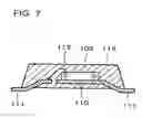
FIG. 8 is a cross-sectional view showing a semiconductor device disclosed in Japanese Laid-open patent publication No. H11-177007 (patent document 1). In FIG. 8, the back electrode of the semiconductor chip 102 and the lead frame 110 are mechanically and electrically connected by a brazing material 116, so that the semiconductor chip 102 is placed on the lead frame 110. A protruding electrode 114 formed on a surface electrode 103 of the semiconductor chip 102 and the lead 111 are mechanically and electrically connected. Further, the semiconductor chip 102, the lead frame 110 and the lead 111 are sealed in the sealing resin 113, exposing only an end portion of the lead 111.
FIG. 9 is a cross-sectional view showing a semiconductor device disclosed in Japanese Laid-open patent publication No. 2000-243880 (patent document 2). In FIG. 9, the semiconductor chip 102 is placed on the lead frame 110 in a similar manner to FIG. 8. On each of the surface electrode 103 of the semiconductor chip 102 and the lead frame 110, a post electrode 115 is fixed by the brazing material 116. Further, the semiconductor chip 102, the lead frame 110 and the post electrode 115 are sealed in the sealing resin 113, exposing an end portion of the post electrode 115.
FIG. 10 is a cross-sectional view showing a semiconductor device disclosed in Japanese Laid-open patent publications No. 2000-277542 and No. 2005-051267 (patent documents 3 and 4). In FIG. 10, the semiconductor chip 102 is placed on the lead frame 110 in a similar manner to FIGS. 8 and 9. Here, an end portion of the lead frame 110 is bent at a right angle toward the side on which the semiconductor chip 102 is placed. On the surface electrode 103 of the semiconductor chip 102, the protruding electrode 114 is provided. Further, an edge 110a of the bent portion of the lead frame 110 and a top portion of the protruding electrode 114 are flush (on a plane parallel to the surface of the lead frame 110 on which the semiconductor chip 102 is placed), and both serve as an external electrode.
SUMMARY OF THE INVENTIONThe semiconductor devices shown in FIGS. 7 to 10, however, may incur stress strain because of a difference in thermal expansion coefficient between the semiconductor chip 102 predominantly constituted of silicon and the lead frame 110 of copper. Such stress strain provokes delamination between the semiconductor chip 102 and the lead frame 110, and breakdown of an adhesive combining the semiconductor chip 102 and the lead frame 110 (for example the brazing material 116 in FIGS. 8 to 10). Consequently, the delamination or the breakdown results in an increase in electrical resistance of the current path connecting the semiconductor chip 102 and the lead frame 110.
According to the present invention, there is provided a semiconductor device comprising a silicon substrate; a semiconductor chip placed on a surface of the silicon substrate; a first protruding electrode provided on a surface of the semiconductor chip opposite to the silicon substrate; a second protruding electrode provided on the surface of the silicon substrate; wherein a top portion of the first protruding electrode and that of the second protruding electrode are of a generally same height from the surface of the silicon substrate.
The semiconductor device thus constructed includes the silicon substrate for placing thereon the semiconductor chip. Such structure prevents emergence of stress strain originating from a difference in linear expansion coefficient between the semiconductor chip and the silicon substrate.
Thus, the present invention provides a semiconductor device that suppresses the stress strain between a semiconductor chip and a substrate carrying the semiconductor chip, and a circuit board provided with such semiconductor device.
BRIEF DESCRIPTION OF THE DRAWINGSThe above and other objects, advantages and features of the present invention will be more apparent from the following description taken in conjunction with the accompanying drawings, in which:
FIG. 1 is a perspective view showing a semiconductor device according to an embodiment of the present invention;
FIG. 2 is a side view showing the semiconductor device according to the embodiment;
FIG. 3 is a side view showing a manufacturing process of the semiconductor device according to the embodiment;
FIGS. 4A to 4C are side views progressively showing a manufacturing process of the semiconductor device of FIGS. 1 and 2;
FIG. 5 is a side view showing a variation of the semiconductor device according to the embodiment;
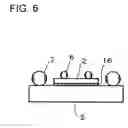
FIG. 6 is a side view showing another variation of the semiconductor device according to the embodiment;
FIG. 7 is a cross-sectional view showing a conventional semiconductor device;
FIG. 8 is a cross-sectional view showing a semiconductor device disclosed in the patented document 1;
FIG. 9 is a cross-sectional view showing a semiconductor device disclosed in the patented document 2;
FIG. 10 is a cross-sectional view showing a semiconductor device disclosed in the patented documents 3 and 4; and
FIG. 11 is a side view showing a circuit board according to an embodiment of the present invention.
DETAILED DESCRIPTIONThe invention will be now described herein with reference to illustrative embodiments. Those skilled in the art will recognize that many alternative embodiments can be accomplished using the teachings of the present invention and that the invention is not limited to the embodiments illustrated for explanatory purposes.
Hereunder, exemplary embodiments of a semiconductor device and a method of manufacturing the same according to the present invention will be described in details, referring to the accompanying drawings. In the drawings, same constituents are given the identical numerals, and duplicating description may be omitted where appropriate.
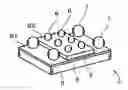
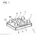
FIG. 1 is a perspective view showing a semiconductor device according to an embodiment of the present invention. FIG. 2 is a side view showing the semiconductor device according to the embodiment. The semiconductor device 1 includes a silicon substrate 5, a semiconductor chip 2 placed on a surface S1 of the silicon substrate 5, a protruding electrode 6 (first protruding electrode) provided on a surface S2 of the semiconductor chip 2 opposite to the silicon substrate 5, and another protruding electrode 7 (second protruding electrode) provided on the surface S1 of the silicon substrate 5.
The semiconductor chip 2 includes a surface electrode (not shown) formed on the surface S2 and a back electrode (not shown) formed on the opposite surface. The protruding electrode 6 is located on the surface electrode. The back electrode of the semiconductor chip 2 is mechanically and electrically connected to the silicon substrate 5 as shown in FIG. 2, by a brazing material 16. The brazing material 16 may be a cream solder or a conductive adhesive.
It is preferable that the semiconductor chip 2 and the silicon substrate 5 are constituted of a same material. In this embodiment, both the semiconductor chip 2 and the silicon substrate 5 are constituted of silicon. That is, the semiconductor substrate included in the semiconductor chip 2 is a silicon substrate. Over the surface S1 of the silicon substrate 5, a conductive layer 8, for example constituted of aluminum, is provided. The conductive layer 8 may be formed by a sputtering or a chemical vapor deposition (CVD) process. It is preferable to provide a coating such as NiAu plating in advance, on a region of the surface of the conductive layer 8 where the protruding electrode 7 is to be formed.
Top portions of the protruding electrodes 6, 7 are of the generally same height (indicated by h in FIG. 2) from the surface S1 of the silicon substrate 5. In other words, the top portions of the protruding electrodes 6, 7 are flush on a plane parallel to the surface S1 of the silicon substrate 5. The protruding electrode 7 located in a region other than where the semiconductor chip 2 is provided, on the surface S1 of the silicon substrate 5. When the semiconductor chip elaborated in the semiconductor chip 2 is a power MOSFET for example, the protruding electrode 6 is connected to the source and the gate thereof, and the protruding electrode 7 is connected to the drain via the silicon substrate 5. Preferably, the both protruding electrodes 6, 7 may be solder ball electrodes.
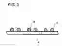
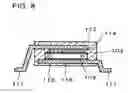
Referring to FIGS. 3 and 4A to 4C, a method of manufacturing the semiconductor device 1 will be described. Firstly, the protruding electrode 6 is formed on a chip-forming surface of a semiconductor wafer 4 (FIG. 3). Then the semiconductor wafer 4 is diced at positions indicated by dash-dot-dot lines in FIG. 3, to be split into the individual semiconductor chip 2. In FIG. 4A, the brazing material 16 is printed on positions where the semiconductor chips 2 are to be placed, on a front surface of the silicon substrate 5a where the conductive layer 8 is provided. In FIG. 4B, the protruding electrodes 7 are formed on predetermined positions on the conductive layer 8. Then the semiconductor chips 2 are fixed on the front surface of the silicon substrate 5a, by the brazing material 16 (FIG. 4C). Upon dicing the silicon substrate 5a at positions indicated by dash-dot-dot lines in FIG. 4C, the semiconductor device 1 is obtained.
Here, the protruding electrode 7 may be formed after placing the semiconductor chip 2 on the silicon substrate 5a. Also, the protruding electrodes 6, 7 may be both formed after placing the semiconductor chip 2 on the silicon substrate 5a. Such method allows continuously forming the protruding electrodes 6, 7, thereby making the manufacturing process simpler and easier. In particular, the protruding electrodes 6, 7 may be formed at a time, which further simplifies the manufacturing process.
FIG. 11 is a side view showing a circuit board according to an embodiment of the present invention. The circuit board includes the semiconductor device 1, and a printed circuit board 20 connected to the protruding electrodes 6, 7 of the semiconductor device 1. In other words, the semiconductor device 1 is mounted on the printed circuit board 20 in a face-down orientation. On this circuit board, the protruding electrodes 6, 7 are exposed.
The foregoing embodiment provides the following advantages. The semiconductor device 1 includes the silicon substrate 5, for placing thereon the semiconductor chip 2. Such structure prevents emergence of stress strain originating from a difference in linear expansion coefficient between the semiconductor chip 2 and the silicon substrate 5.
Such stress strain may provoke delamination between the semiconductor chip 2 and the silicon substrate 5, and breakdown of the brazing material 16 combining the semiconductor chip 2 and the silicon substrate 5. Consequently, the delamination or the breakdown results in an increase in electrical resistance of the current path (for example the resistance of the back electrode of the semiconductor chip 2) connecting the semiconductor chip 2 and the silicon substrate 5. Suppressing such stress strain is, therefore, quite important.
In the semiconductor device 1, the semiconductor chip 2 is placed on the silicon substrate 5, instead of on a lead frame, which eliminates the need to provide a sealing resin. This prevents degradation in heat dissipation efficiency of the semiconductor device 1, which would otherwise be incurred by the sealing resin. Actually, the semiconductor device 1 is not provided with the sealing resin. Here, a resin may be provided on the surface S1 of the silicon substrate 5, for the purpose of reinforcing the semiconductor device 1. Even so, however, the back surface of the silicon substrate 5 (opposite to the surface S1) is not covered with the resin, and hence heat generated in the semiconductor chip 2 can be effectively dispersed through the side of the silicon substrate 5.
In the semiconductor devices shown in FIGS. 7 to 9, the semiconductor chip 102 and the lead frame 110 are covered with the sealing resin 113. Accordingly, those semiconductor devices have a room for improvement in the aspect of heat dissipation.
Further, the electrodes provided for the semiconductor chip 2 and the silicon substrate 5 are protruding electrodes (protruding electrodes 6, 7). Accordingly, when implementing the semiconductor device 1 on a substrate or the like, the electrodes can be connected to the substrate under the same condition. Therefore, the structure of the semiconductor device 1 facilitates the implementing process.
In contrast, the semiconductor device shown in FIG. 10 includes the electrodes of different natures, namely the protruding electrode 114 made of a solder bump or a solder ball and the edge 110a which is not provided with the solder. This makes it difficult to connect the protruding electrode 114 and the 110a to a printed circuit board or the like under the same condition, when implementing the semiconductor device on the board. Besides, an additional process of applying a cream solder to the edge 110a may have to be performed. The semiconductor device of FIG. 10, therefore, has a room for improvement in the aspect of implementation simpleness.
The application process of the cream solder to the edge 110a cannot be skipped even when, for example, all other components to be implemented (components to be mounted on the circuit board together with the semiconductor device 1) are semiconductor devices including solder ball electrodes such as a ball grid array (BGA) and a flip-chip (FC). Moreover, when the cream solder has to be applied to the circuit board such as a case that all other components to be implemented are of a lead type or a leadless chip carrier (LCC), or when the semiconductor devices are press-bonded to the circuit board by heat or pressure, it becomes difficult to unify the implementing conditions because of, for example, a difference in melting point between the protruding electrode 114 and the cream solder.
The protruding electrodes 6, 7 are the solder ball electrodes. Such structure permits skipping the cream solder application process to the circuit board, when all other components to be implemented are semiconductor devices including solder ball electrodes such as a BGA and a FC.
It is not, however, imperative that the protruding electrodes 6, 7 are the solder ball electrodes. The protruding electrode 6 may be a stud bump electrode, a post electrode, or a bump electrode. The stud bump electrode may be formed by bonding a fine metal wire. The post electrode may be formed by erecting a metal post on the semiconductor chip 2. The bump electrode may be formed by a plating process. Also, the protruding electrode 7 may be a post electrode or a bump electrode. The bump electrode corresponds to a post electrode in which the ratio of the height to the base is relatively small, and is in a shape, for instance, like a board, a disk or a hill.
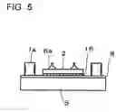
In FIG. 5 for example, a stud bump electrode 6a is provided as the first protruding electrode, and a post electrode 7a as the second protruding electrode. Such structure allows unifying the implementing process even when the cream solder has to be applied for implementing other components, or when heat or pressure is employed for press-bonding the semiconductor device on the circuit board. The stud bump electrode 6a is formed in the same way as ordinary wire bonding using ultrasonic waves or thermo compression bonding, where no brazing material is used. The post electrode 7a may be formed by a plating process without a brazing material used.
When the protruding electrodes 6, 7 are post electrodes, it is preferable to form the protruding electrodes 6, 7 directly on the semiconductor chip 2 and the silicon substrate 5 respectively. Such method enables more accurately forming the post electrodes at desired positions, than forming the post electrodes via the brazing material as shown in FIG. 9. For example, a plating process may be employed, for forming the post electrode directly on the semiconductor chip 2 and the silicon substrate 5.
Further, since the semiconductor device 1 can be manufactured through a simpler process than the semiconductor devices shown in FIGS. 7 to 9, no increase in cost is incurred. Also, unlike the semiconductor devices shown in FIGS. 7 and 8, the lead is not sticking out of the sealing resin, which leads to reduced footprint of the device. Furthermore, all the external electrodes (protruding electrodes 6, 7) are constituted of a same metal material, and formed so that the top portions thereof become flush on the same plane. Such configuration allows implementing the semiconductor device 1 with other components under the same conditions.
The circuit board shown in FIG. 11 is provided with the semiconductor device 1 which is free from a sealing resin, and hence has excellent heat dissipation efficiency. In the circuit board, besides, the protruding electrodes 6, 7 are exposed. Such configuration provides even higher heat dissipation efficiency, compared with a case that a resin such as an underfill resin is loaded between the semiconductor device 1 and the printed circuit board 20.
Still further, since the electrodes provided for the semiconductor chip 2 and the silicon substrate 5 are both protruding electrodes (protruding electrodes 6, 7) as already stated, the semiconductor device 1 can be easily implemented on the printed circuit board 20. Thus, a circuit board easy to fabricate is provided.
The semiconductor device and the circuit board according to the present invention are not limited to the foregoing embodiment, but various modifications may be made. For example, a plurality of semiconductor chips 2 may be provided on the silicon substrate 5. In other words, a plurality of semiconductor chips may be loaded on the silicon substrate 5 if need be, so as to constitute a module.
It is apparent that the present invention is not limited to the above embodiment, and may be modified and changed without departing from the scope and spirit of the invention.
Claims
What is claimed is:1. A semiconductor device comprising:
a silicon substrate;
a semiconductor chip placed on a surface of said silicon substrate;
a first protruding electrode provided on a surface of said semiconductor chip opposite to said silicon substrate;
a second protruding electrode provided on said surface of said silicon substrate;
wherein a top portion of said first protruding electrode and that of said second protruding electrode are of a generally same height from said surface of said silicon substrate.
2. The semiconductor device according to claim 1, wherein said semiconductor chip includes a back electrode connected to said silicon substrate.
3. The semiconductor device according to claim 1, wherein said first and second protruding electrodes are solder ball electrodes.
4. The semiconductor device according to claim 1, wherein said first and second protruding electrodes are post electrodes.
5. The semiconductor device according to claim 1, wherein said first and second protruding electrodes are provided without a brazing material on said semiconductor chip and said silicon substrate respectively.
6. The semiconductor device according to claim 1, wherein a plurality of said semiconductor chips are provided on said silicon substrate.
7. A circuit board comprising:
said semiconductor device according to claim 1; and
a printed circuit board connected to said first and second protruding electrodes.
8. The circuit board according to claim 7, wherein said first and second protruding electrodes are exposed.
Images & Drawings included:


Sources:
- United States Patent and Trademark Office - verify current appl. status at the USPTO↗
Similar patent applications:
- » 20250105121
SEMICONDUCTOR DEVICE, CIRCUIT BOARD, AND SEMICONDUCTOR DEVICE MANUFACTURING METHOD - » 20130015582
Circuit board, semiconductor device, process for manufacturing circuit board and process for manufacturing semiconductor device - » 20170250141
WIRING CIRCUIT BOARD, SEMICONDUCTOR DEVICE, METHOD OF MANUFACTURING WIRING CIRCUIT BOARD, AND METHOD OF MANUFACTURING SEMICONDUCTOR DEVICE - » 20090174062
CIRCUIT BOARD, SEMICONDUCTOR DEVICE, AND MANUFACTURING METHOD OF CIRCUIT BOARD - » 20230134246
CIRCUIT BOARD, SEMICONDUCTOR DEVICE, AND METHOD OF MANUFACTURING CIRCUIT BOARD - » 20070145518
Circuit board, semiconductor device, and manufacturing method of circuit board - » 20220369454
Circuit board, semiconductor device and method of manufacturing circuit board - » 20150257252
Semiconductor circuit board, semiconductor device using the same, and method for manufacturing semiconductor circuit board - » 20250073826
METHOD FOR PRODUCING ACTIVE METAL PASTE, METHOD FOR PRODUCING CERAMIC CIRCUIT BOARD, METHOD FOR PRODUCING SEMICONDUCTOR DEVICE, ACTIVE METAL PASTE, CERAMIC CIRCUIT BOARD, AND SEMICONDUCTOR DEVICE - » 20140376202
Printed circuit board, semiconductor device connection structure, and method of manufacturing a printed circuit board
Recent applications in this class:
- » 20250157866 2025-05-15
SILICON-ON-INSULATOR DEVICE INCLUDING CARRIER STRUCTURE - » 20250054822 2025-02-13
INTEGRATED CIRCUIT DEVICE AND METHOD OF MANUFACTURING THE SAME - » 20250006568 2025-01-02
INTEGRATED CIRCUIT STRUCTURES HAVING ALTERNATIVE CARRIERS FOR DUAL-SIDED DEVICES - » 20230386947 2023-11-30
SEMICONDUCTOR DEVICE AND METHOD - » 20230274992 2023-08-31
SILICON NITRIDE SUBSTRATE, SILICON NITRIDE CIRCUIT SUBSTRATE, AND EVALUATION METHOD, EVALUATION DEVICE, AND EVALUATION SYSTEM FOR SILICON NITRIDE SUBSTRATE AND SILICON NITRIDE CIRCUIT SUBSTRATE - » 20230116302 2023-04-13
SEMICONDUCTOR CHIP AND METHOD FOR MANUFACTURING THE SAME - » 20230034867 2023-02-02
WIRING SUBSTRATE AND METHOD OF MANUFACTURING THE SAME - » 20210249318 2021-08-12
Semiconductor device and method - » 20190348337 2019-11-14
Semiconductor device and method - » 20190221489 2019-07-18
Insulating substrate and semiconductor device using same
Recent applications for this Assignee:
- » 20120096421 2012-04-19
Semiconductor integrated circuit design apparatus and method for analyzing a delay in a semiconductor integrated circuit - » 20110131397 2011-06-02
MULTIPROCESSOR SYSTEM AND MULTIPROCESSOR CONTROL METHOD - » 20110070741 2011-03-24
METHOD OF CLEANING PLASMA ETCHING APPARATUS - » 20110050761 2011-03-03
PIXEL CIRCUIT AND DISPLAY DEVICE - » 20110050746 2011-03-03
Level shift circuit, and driver and display device using the same - » 20110049632 2011-03-03
Semiconductor device - » 20110032128 2011-02-10
ANALOG-DIGITAL CONVERTER CIRCUIT AND CALIBRATION METHOD - » 20110032031 2011-02-10
Amplifier circuit and light receiving amplifier circuit using the same - » 20110024865 2011-02-03
SEMICONDUCTOR LIGHT RECEIVING DEVICE - » 20110024832 2011-02-03
Vertical power MOSFET semiconductor apparatus having separate base regions and manufacturing method thereof