Bump structure and its forming method
US20070080452A1
2007-04-12
11/514,329
2006-09-01
Abstract:
A bump structure mainly includes a metal core, a buffer encapsulant, and a metal cap where the metal core is a stud bump formed by wire bonding. The buffer encapsulant encapsulates the metal core. A metal cap is formed on the top surface of the buffer encapsulant and is electrically connected to the metal core. Therefore, the bump structure possesses excellent resistance of thermal stress to reduce or even eliminate metal fatigue in the bump without causing electrical shorts in the package.
Inventors:
- Chun-Ying Lin 5 🇹🇼 Tainan, Taiwan
- Hsiang-Ming Huang 12 🇹🇼 Tainan, Taiwan
- An-Hong Liu 25 🇹🇼 Tainan, Taiwan
- Yi-Chang Lee 14 🇹🇼 Tainan, Taiwan
- Chen-Ya- Chi 1 🇹🇼 Tainan, Taiwan
Interested in similar patents?
Get notified when new applications in this technology area are published.
Classification:
H01L24/10 » CPC main
Arrangements for connecting or disconnecting semiconductor or solid-state bodies; Methods or apparatus related thereto; Means for bonding being attached to, or being formed on, the surface to be connected, e.g. chip-to-package, die-attach, "first-level" interconnects; Manufacturing methods related thereto Bump connectors ; Manufacturing methods related thereto
H01L24/13 » CPC further
Arrangements for connecting or disconnecting semiconductor or solid-state bodies; Methods or apparatus related thereto; Means for bonding being attached to, or being formed on, the surface to be connected, e.g. chip-to-package, die-attach, "first-level" interconnects; Manufacturing methods related thereto; Bump connectors ; Manufacturing methods related thereto; Structure, shape, material or disposition of the bump connectors prior to the connecting process of an individual bump connector
H05K3/4007 » CPC further
Apparatus or processes for manufacturing printed circuits; Forming printed elements for providing electric connections to or between printed circuits Surface contacts, e.g. bumps
H05K3/4007 » CPC further
Apparatus or processes for manufacturing printed circuits; Forming printed elements for providing electric connections to or between printed circuits Surface contacts, e.g. bumps
H01L2224/05573 » CPC further
Indexing scheme for arrangements for connecting or disconnecting semiconductor or solid-state bodies and methods related thereto as covered by; Means for bonding being attached to, or being formed on, the surface to be connected, e.g. chip-to-package, die-attach, "first-level" interconnects; Manufacturing methods related thereto; Bonding areas; Manufacturing methods related thereto; Structure, shape, material or disposition of the bonding areas prior to the connecting process of an individual bonding area; External layer Single external layer
H01L2224/13099 » CPC further
Indexing scheme for arrangements for connecting or disconnecting semiconductor or solid-state bodies and methods related thereto as covered by; Means for bonding being attached to, or being formed on, the surface to be connected, e.g. chip-to-package, die-attach, "first-level" interconnects; Manufacturing methods related thereto; Bump connectors; Manufacturing methods related thereto; Structure, shape, material or disposition of the bump connectors prior to the connecting process of an individual bump connector; Core members of the bump connector Material
H01L2924/01005 » CPC further
Indexing scheme for arrangements or methods for connecting or disconnecting semiconductor or solid-state bodies as covered by; Chemical elements Boron [B]
H01L2924/01006 » CPC further
Indexing scheme for arrangements or methods for connecting or disconnecting semiconductor or solid-state bodies as covered by; Chemical elements Carbon [C]
H01L2924/01013 » CPC further
Indexing scheme for arrangements or methods for connecting or disconnecting semiconductor or solid-state bodies as covered by; Chemical elements Aluminum [Al]
H01L2924/01029 » CPC further
Indexing scheme for arrangements or methods for connecting or disconnecting semiconductor or solid-state bodies as covered by; Chemical elements Copper [Cu]
H01L2924/01033 » CPC further
Indexing scheme for arrangements or methods for connecting or disconnecting semiconductor or solid-state bodies as covered by; Chemical elements Arsenic [As]
H01L2924/01078 » CPC further
Indexing scheme for arrangements or methods for connecting or disconnecting semiconductor or solid-state bodies as covered by; Chemical elements Platinum [Pt]
H01L2924/01079 » CPC further
Indexing scheme for arrangements or methods for connecting or disconnecting semiconductor or solid-state bodies as covered by; Chemical elements Gold [Au]
H01L2924/01082 » CPC further
Indexing scheme for arrangements or methods for connecting or disconnecting semiconductor or solid-state bodies as covered by; Chemical elements Lead [Pb]
H01L2924/014 » CPC further
Indexing scheme for arrangements or methods for connecting or disconnecting semiconductor or solid-state bodies as covered by; Alloys Solder alloys
H05K3/4015 » CPC further
Apparatus or processes for manufacturing printed circuits; Forming printed elements for providing electric connections to or between printed circuits; Surface contacts, e.g. bumps using auxiliary conductive elements, e.g. pieces of metal foil, metallic spheres
H05K3/4015 » CPC further
Apparatus or processes for manufacturing printed circuits; Forming printed elements for providing electric connections to or between printed circuits; Surface contacts, e.g. bumps using auxiliary conductive elements, e.g. pieces of metal foil, metallic spheres
H05K2201/0347 » CPC further
Indexing scheme relating to printed circuits covered by; Conductive materials; Structure of the conductor; Layered conductors or foils Overplating, e.g. for reinforcing conductors or bumps; Plating over filled vias
H05K2201/0347 » CPC further
Indexing scheme relating to printed circuits covered by; Conductive materials; Structure of the conductor; Layered conductors or foils Overplating, e.g. for reinforcing conductors or bumps; Plating over filled vias
H05K2201/0367 » CPC further
Indexing scheme relating to printed circuits covered by; Conductive materials; Structure of the conductor; Conductor shape Metallic bump or raised conductor not used as solder bump
H05K2201/0367 » CPC further
Indexing scheme relating to printed circuits covered by; Conductive materials; Structure of the conductor; Conductor shape Metallic bump or raised conductor not used as solder bump
H05K2201/10977 » CPC further
Indexing scheme relating to printed circuits covered by; Details of components or other objects attached to or integrated in a printed circuit board; Details of electrical connections of non-printed components, e.g. special leads; Other details of electrical connections Encapsulated connections
H05K2203/049 » CPC further
Indexing scheme relating to apparatus or processes for manufacturing printed circuits covered by; Soldering or other types of metallurgic bonding Wire bonding
H05K2203/049 » CPC further
Indexing scheme relating to apparatus or processes for manufacturing printed circuits covered by; Soldering or other types of metallurgic bonding Wire bonding
H05K2203/0597 » CPC further
Indexing scheme relating to apparatus or processes for manufacturing printed circuits covered by; Patterning and lithography; Masks; Details of resist; Details of resist Resist applied over the edges or sides of conductors, e.g. for protection during etching or plating
H05K2203/0597 » CPC further
Indexing scheme relating to apparatus or processes for manufacturing printed circuits covered by; Patterning and lithography; Masks; Details of resist; Details of resist Resist applied over the edges or sides of conductors, e.g. for protection during etching or plating
H01L2224/13 » CPC further
Indexing scheme for arrangements for connecting or disconnecting semiconductor or solid-state bodies and methods related thereto as covered by; Means for bonding being attached to, or being formed on, the surface to be connected, e.g. chip-to-package, die-attach, "first-level" interconnects; Manufacturing methods related thereto; Bump connectors; Manufacturing methods related thereto; Structure, shape, material or disposition of the bump connectors prior to the connecting process of an individual bump connector
H01L2924/351 » CPC further
Indexing scheme for arrangements or methods for connecting or disconnecting semiconductor or solid-state bodies as covered by; Technical effects; Mechanical effects Thermal stress
H01L2924/00 » CPC further
Indexing scheme for arrangements or methods for connecting or disconnecting semiconductor or solid-state bodies as covered by
H01L2924/00014 » CPC further
Indexing scheme for arrangements or methods for connecting or disconnecting semiconductor or solid-state bodies as covered by; Technical content checked by a classifier the subject-matter covered by the group, the symbol of which is combined with the symbol of this group, being disclosed without further technical details
H01L2224/05599 » CPC further
Indexing scheme for arrangements for connecting or disconnecting semiconductor or solid-state bodies and methods related thereto as covered by; Means for bonding being attached to, or being formed on, the surface to be connected, e.g. chip-to-package, die-attach, "first-level" interconnects; Manufacturing methods related thereto; Bonding areas; Manufacturing methods related thereto; Structure, shape, material or disposition of the bonding areas prior to the connecting process of an individual bonding area; External layer Material
H01L23/48 IPC
Details of semiconductor or other solid state devices Arrangements for conducting electric current to or from the solid state body in operation, e.g. leads, terminal arrangements ; Selection of materials therefor
H01L23/52 IPC
Details of semiconductor or other solid state devices Arrangements for conducting electric current within the device in operation from one component to another, i.e. interconnections, e.g. wires, lead frames
H01L29/40 IPC
Semiconductor devices adapted for rectifying, amplifying, oscillating or switching, or capacitors or resistors with at least one potential-jump barrier or surface barrier, e.g. PN junction depletion layer or carrier concentration layer; Details of semiconductor bodies or of electrodes thereof; Multistep manufacturing processes therefor Electrodes ; Multistep manufacturing processes therefor
H01L21/44 IPC
Processes or apparatus adapted for the manufacture or treatment of semiconductor or solid state devices or of parts thereof; Manufacture or treatment of semiconductor devices or of parts thereof the devices having at least one potential-jump barrier or surface barrier, e.g. PN junction, depletion layer or carrier concentration layer the devices having semiconductor bodies not provided for in groups, , , and with or without impurities, e.g. doping materials Manufacture of electrodes on semiconductor bodies using processes or apparatus not provided for in groups -
Description
FIELD OF THE INVENTIONThe present invention relates to a semiconductor device, and more particularly to a bump structure and its forming method.
BACKGROUND OF THE INVENTIONRecently, more and more semiconductor devices run at higher frequencies such as CPU, DDR2, or DDR3 DRAM, so that the conventional packages can not meet the requirements of high speed applications. The flip chip packages and the wafer-level packages (WLP) have been developed for high speed applications to reduce the transmitting lengths between the chip and the substrate to increase the operation frequencies. As revealed in R.O.C. Taiwan Patent publication No. 200518289, conventional bumps are solder bumps or metal plated bumps such as gold, aluminum, copper, etc. Since the coefficients of thermal expansion (CTE) of chips and substrates are different due to different materials, bumps will experience thermal stresses during temperature changes. Eventually metal fatigue will induce in the bumps leading to bump breakage and failure leading to electrical shorts in the packages.
SUMMARY OF THE INVENTIONThe main purpose of the present invention is to provide a bump structure including a metal core formed by wire bonding and encapsulated by a buffer encapsulant. A metal cap is formed on top of the buffer encapsulant to electrically connect to the metal core. Accordingly, a composite bump with excellent resistance of thermal stresses is formed to reduce or even eliminate metal fatigue in the bump without causing electrical shorts in the package.
According to the present invention, a bump structure comprises a metal core, a buffer encapsulant, and a metal cap, where the metal core is a stud bump formed by wire bonding and is encapsulated by the buffer encapsulant. The buffer encapsulant has a top surface where a metal cap is formed on the top surface to electrically connect to the metal core.
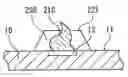
DESCRIPTION OF THE DRAWINGSFIG. 1 shows a cross sectional view of a bump structure disposed on a substrate according to the first embodiment of the present invention.
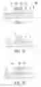
FIG. 2A to 2C shows cross sectional views of the bump structure during fabrication processes according to the first embodiment of the present invention.
FIG. 3 shows a cross sectional view of another bump structure disposed on a substrate according to the second embodiment of the present invention.
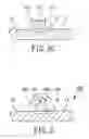
FIG. 4A to 4C shows cross sectional views of the bump structure during fabrication processes according to the second embodiment of the present invention.
DETAIL DESCRIPTION OF THE INVENTIONPlease refer to the attached drawings, the present invention will be described by means of embodiment(s) below.
According to the first embodiment of the present invention, a bump structure is illustrated in FIG. 1. A bump structure 100 is disposed on a substrate 10 as an electrical terminal, which comprises a metal core 110, a buffer encapsulant 120 and a metal cap 130. The metal core 110 is a stud bump formed by wire bonding and is attached to the bonding pad 12 of the substrate 10. The material of the metal core 110 is selected from the group consisting of gold, aluminum, copper, and tin-lead, and normally is gold. The buffer encapsulant 120 has a top surface 121 and encapsulates the metal core 10. In the present embodiment, the buffer encapsulant 120 is in B-stage and can be formed by printing. The metal cap 130 is formed on the top surface 121 of the buffer encapsulant 120 and is electrically connected to the metal core 110. The material of the metal cap 130 is selected from the group of tin, tin-lead, copper, nickel, and gold. In this embodiment, the metal cap 130 is a copper pad plated with nickel and gold. Therefore, the bump structure 100 is a composite bump with excellent resistance of thermal stresses to reduce or even eliminate metal fatigue in the bump without causing electrical shorts in the package. Preferably, the area of the metal cap 130 is smaller than the top surface 121 of the buffer encapsulant 120 without covering the sidewalls of the buffer encapsulant 120 to avoid delamination from the buffer encapsulant 120.
The fabrication processes of the bump structure 100 disposed on the substrate 10 are revealed from FIG. 2A to FIG. 2C. Firstly, as shown in FIG. 2A, a substrate 10 is provided where the substrate is selected from the group consisting of wafers, chips, semiconductor packages, printed circuit boards, and flexible printed circuit boards. The substrate 10 has a top surface 11 on which at least a bonding pad 12 is formed. Utilizing wire bonding technology, a stud bump is formed on the bonding pad 12 of the substrate 10 to be the metal core 110 of the bump structure 100. Then, as shown in FIG. 2B, a buffer encapsulant 120 is formed on the top surface 11 of the substrate 10 by stencil printing corresponding to the bonding pad 12 to encapsulate the metal core 110. The buffer encapsulant 120 has a top surface 121. In the present embodiment, the metal core 110 has a tip protruded from the top surface 121 of the buffer encapsulant 120. Preferably, as shown in FIG. 2C, the protruded portion of the metal core 110 is removed by a grounding step to planarize the top surface 121 of the buffer encapsulant 120 and to partially expose the metal core 110. Finally, as shown in FIG. 1, a metal cap 130 is disposed on the top surface 121 of the buffer encapsulant 120 by printing or plating or sputtering so that the metal cap 130 is electrically connected to the metal core 100. The bump structure 100 is fabricated.
Another bump structure 200 is revealed in FIG. 3 according to the second embodiment of the present invention. A bump structure 200 is disposed to the bonding pad 12 of the substrate 10 and comprises a metal core 210, a buffer encapsulant 220, and a metal cap 230 where the metal core 210 is a stud bump formed by wire bonding. The metal core 210 and the buffer encapsulant 220 are deformable and flexible such that the metal cap 230 is movable with respect with corresponding bonding pad 12 of the substrate 10. In this embodiment, the metal core 210 is a stud bump or a stack of multiply stud bumps. The buffer encapsulant 220 encapsulates the metal core 210 with the metal core 210 protruding from the top surface 221 of the buffer encapsulant 220. Normally, the buffer encapsulant 220 is in B-stage. The metal cap 230 is formed on the top surface 221 of the buffer encapsulant 220 to electrically connect to the metal core 210 where the metal cap 230 is formed by printing, plating, or sputtering. Preferably, the area of the metal cap 230 is smaller than the top surface 221 of the buffer encapsulant 220. The materials of the metal cap 230 is selected from the group of tin, lead, copper, nickel, or gold. Therefore, the bump structure 200 is a composite bump with excellent resistance of thermal stresses to reduce or even eliminate metal fatigue in the bump without causing electrical shorts in the package.
The fabrication processes of the bump structure 200 disposed on the substrate 10 are shown from FIG. 4A to 4C. Firstly, as shown in FIG. 4A, a substrate 10 is provided, which has a top surface 11 and at least a bonding pad 12. A metal core 210 of the bump structure 200 is a stud bump formed on the bonding pad 12 of the substrate 10 by wire bonding. Then, as shown in FIG. 4B, a buffer encapsulant 220 is formed on the top surface 11 of the substrate 10 to encapsulate the metal core 210 where the buffer encapsulant 220 is formed by spin coating, printing, or curtain coating to fully cover the top surface 11 of the substrate 10. The buffer encapsulant 220 has a top surface 221 where the metal core 210 is protruded from the top surface 221. Then, as shown in FIG. 4C, the buffer encapsulant 220 is patterned by photolithography to remove the unwanted portions of the buffer encapsulant 220 to form bump-like structures where the buffer encapsulant 220 is a photo-sensitive dielectric material such as polyimide (PI) or benzocyclobutene (BCB). Finally, a metal cap 230 is formed on the top surface 221 of the buffer encapsulant 220 by printing to encapsulate the exposed portion of the metal core 210 to electrically connect the metal cap 230
The above description of embodiments of this invention is intended to be illustrative and not limiting. Other embodiments of this invention will be obvious to those skilled in the art in view of the above disclosure.
Claims
What is claimed is:1. A bump structure disposed on a substrate, comprising:
a metal core formed by wire-bonding wherein the metal core is a stud bump;
a buffer encapsulant encapsulating the metal core and having a top surface; and
a metal cap formed on the top surface of the buffer encapsulant and electrically connected to the metal core.
2. The bump structure of claim 1, wherein the materials of metal core is selected from the group consisting of gold, aluminum, copper, and tin-lead.
3. The bump structure of claim 1, wherein the materials of metal core is selected from the group consisting of tin, tin-lead, copper, nickel, and gold.
4. The bump structure of claim 1, wherein the buffer encapsulant is in B-stage.
5. The bump structure of claim 1, wherein the buffer encapsulant is made of polyimide (PI) or benzocyclobutene (BCB).
6. The bump structure of claim 1, wherein the metal core is attached to a bonding pad of the substrate, wherein the substrate is selected from the group consisting of wafer, chip, semiconductor package, printed circuit board, and flexible printed circuit board.
7. The bump structure of claim 1, wherein the buffer encapsulant is formed by printing, spin coating, or curtain coating.
8. The bump structure of claim 1 , wherein the metal cap is formed by printing, plating, or sputtering.
9. The bump structure of claim 1, wherein the area of the metal cap is smaller than the top surface of the buffer encapsulant.
10. A fabrication method of a bump structure, including:
providing a substrate having at least a bonding pad;
wire-bonding a stud bump on the bonding pad of the substrate to form a metal core;
forming a buffer encapsulant on the substrate to encapsulate the metal core, wherein the buffer encapsulant has a top surface; and
forming a metal cap on the top surface of the buffer encapsulant, the metal cap be electrically connected to the metal core.
11. The method of claim 10, wherein the buffer encapsulant is in B-stage.
12. The method of claim 10, wherein the substrate is selected from the group consisting of wafer, chip, semiconductor package, printed circuit board, and flexible printed circuit board.
13. The method of claim 10, wherein the buffer encapsulant is formed by printing, spin coating, or curtain coating.
14. The method of claim 13, further comprising a photolithographic process to pattern the buffer encapsulant.
15. The method of claim 14, wherein the buffer encapsulant is photo-sensitive dielectric materials of polyimide (PI) or benzocyclobutene (BCB).
16. The method of claim 10, wherein the metal cap is formed by printing, plating, or sputtering.
17. The method of claim 10, wherein the area of the metal cap is smaller than the top surface of the buffer encapsulant.
18. The method of claim 10, further comprising a grounding step to planarize the top surface of the buffer encapsulant and to expose the metal core.
Images & Drawings included:

Sources:
- United States Patent and Trademark Office - verify current appl. status at the USPTO↗
Similar patent applications:
- » 20070252272
Bump structure, method of forming bump structure, and semiconductor apparatus using the same - » 20130292822
Bump structure, having concave lateral sides, semiconductor package having the bump structure, and method of forming the bump structure - » 20190096836
BUMP STRUCTURE, SEMICONDUCTOR PACKAGE INCLUDING THE BUMP STRUCTURE, AND METHOD OF FORMING THE BUMP STRUCTURE - » 20110006416
Structure and method for forming pillar bump structure having sidewall protection - » 20050208751
Solder bump structure and method for forming a solder bump - » 20060113681
Reinforced solder bump structure and method for forming a reinforced solder bump - » 20120217640
Semiconductor device and method of forming bump structure with insulating buffer layer to reduce stress on semiconductor wafer - » 20120299176
Semiconductor device and method of forming bump structure with multi-layer UBM around bump formation area - » 20070228559
Connecting structure, method for forming bump, and method for producing device-mounting substrate - » 20100140805
Method of forming bump structure having tapered sidewalls for stacked dies
Recent applications in this class:
- » 20250038143 2025-01-30
CHIP - » 20240297134 2024-09-05
ELECTRONIC PACKAGE - » 20240282733 2024-08-22
SEMICONDUCTOR DEVICE WITH DELAMINATION REDUCTION MECHANISM AND METHODS FOR MANUFACTURING THE SAME - » 20240145417 2024-05-02
SEMICONDUCTOR PACKAGE AND METHOD OF FABRICATING THE SAME - » 20240038703 2024-02-01
SEMICONDUCTOR ASSEMBLY INCLUDING MULTIPLE SOLDER MASKS - » 20210272920 2021-09-02
Semiconductor device with backmetal and related methods - » 20210091029 2021-03-25
Shielding structures - » 20190348383 2019-11-14
Monolithic decoupling capacitor between solder bumps - » 20190267344 2019-08-29
Semiconductor device with backmetal and related methods - » 20180286825 2018-10-04
Monolithic decoupling capacitor between solder bumps