Semiconductor package for fine pitch miniaturization and manufacturing method thereof
US20080145967A1
2008-06-19
11/898,717
2007-09-14
✅ Patent granted
US 7,795,071 B2
2010-09-14
-
-
A. Sefer | Ermias Woldegeorgis
2027-09-14
Abstract:
A semiconductor package and a manufacturing method thereof are provided. The package element has a first insulating layer, and a plurality of holes are disposed on the first surface of the first insulating layer. Besides, a plurality of package traces are embedded in the insulating layer and connected to the other end of the holes. The holes function as a positioning setting for connecting the solder balls to the package traces, such that the signal of the semiconductor chip is connected to the package trace via conductor of the chip, and further transmitted externally via solder ball. The elastic modulus of the material of the first insulating layer is preferably larger than 1.0 GPa.
Inventors:
- Hwee-Seng Jimmy Chew 35 🇸🇬 Singapore, Singapore
- Chee-Kian ONG 12 🇸🇬 Singapore, Singapore
- Bin Chichik ABD. RAZAK 4 🇸🇬 Singapore, Singapore
- Chew Hwee-Seng Jimmy 6 🇸🇬 Singapore, Singapore
- Ong Chee Kian 5 🇸🇬 Singapore, Singapore
- Abd. Razak Bin Chichik 7 🇸🇬 Singapore, Singapore
Assignee:
- ADVANPACK SOLUTIONS PTE LTD. 41 🇸🇬 Singapore, Singapore
Interested in similar patents?
Get notified when new applications in this technology area are published.
Classification:
H01L25/0657 » CPC main
Assemblies consisting of a plurality of individual semiconductor or other solid state devices ; Multistep manufacturing processes thereof all the devices being of a type provided for in the same subgroup of groups - , e.g. assemblies of rectifier diodes the devices not having separate containers the devices being of a type provided for in group Stacked arrangements of devices
H01L21/4839 » CPC further
Processes or apparatus adapted for the manufacture or treatment of semiconductor or solid state devices or of parts thereof; Manufacture or treatment of semiconductor devices or of parts thereof the devices having at least one potential-jump barrier or surface barrier, e.g. PN junction, depletion layer or carrier concentration layer; Manufacture or treatment of parts, e.g. containers, prior to assembly of the devices, using processes not provided for in a single one of the subgroups -; Conductive parts; Flat leads, e.g. lead frames with or without insulating supports Assembly of a flat lead with an insulating support, e.g. for TAB
H01L21/4853 » CPC further
Processes or apparatus adapted for the manufacture or treatment of semiconductor or solid state devices or of parts thereof; Manufacture or treatment of semiconductor devices or of parts thereof the devices having at least one potential-jump barrier or surface barrier, e.g. PN junction, depletion layer or carrier concentration layer; Manufacture or treatment of parts, e.g. containers, prior to assembly of the devices, using processes not provided for in a single one of the subgroups -; Conductive parts; Leads on or in insulating or insulated substrates, e.g. metallisation Connection or disconnection of other leads to or from a metallisation, e.g. pins, wires, bumps
H01L21/486 » CPC further
Processes or apparatus adapted for the manufacture or treatment of semiconductor or solid state devices or of parts thereof; Manufacture or treatment of semiconductor devices or of parts thereof the devices having at least one potential-jump barrier or surface barrier, e.g. PN junction, depletion layer or carrier concentration layer; Manufacture or treatment of parts, e.g. containers, prior to assembly of the devices, using processes not provided for in a single one of the subgroups -; Conductive parts; Leads on or in insulating or insulated substrates, e.g. metallisation Via connections through the substrate with or without pins
H01L21/563 » CPC further
Processes or apparatus adapted for the manufacture or treatment of semiconductor or solid state devices or of parts thereof; Manufacture or treatment of semiconductor devices or of parts thereof the devices having at least one potential-jump barrier or surface barrier, e.g. PN junction, depletion layer or carrier concentration layer; Assembly of semiconductor devices using processes or apparatus not provided for in a single one of the subgroups - , e.g. sealing of a cap to a base of a container; Encapsulations, e.g. encapsulation layers, coatings Encapsulation of active face of flip-chip device, e.g. underfilling or underencapsulation of flip-chip, encapsulation preform on chip or mounting substrate
H01L21/6835 » CPC further
Processes or apparatus adapted for the manufacture or treatment of semiconductor or solid state devices or of parts thereof; Apparatus specially adapted for handling semiconductor or electric solid state devices during manufacture or treatment thereof; Apparatus specially adapted for handling wafers during manufacture or treatment of semiconductor or electric solid state devices or components ; Apparatus not specifically provided for elsewhere for supporting or gripping using temporarily an auxiliary support
H01L23/49558 » CPC further
Details of semiconductor or other solid state devices; Arrangements for conducting electric current to or from the solid state body in operation, e.g. leads, terminal arrangements ; Selection of materials therefor consisting of soldered constructions; Lead-frames or other flat leads; Geometry of the lead-frame Insulating layers on lead frames, e.g. bridging members
H01L23/49575 » CPC further
Details of semiconductor or other solid state devices; Arrangements for conducting electric current to or from the solid state body in operation, e.g. leads, terminal arrangements ; Selection of materials therefor consisting of soldered constructions; Lead-frames or other flat leads Assemblies of semiconductor devices on lead frames
H01L23/49816 » CPC further
Details of semiconductor or other solid state devices; Arrangements for conducting electric current to or from the solid state body in operation, e.g. leads, terminal arrangements ; Selection of materials therefor consisting of soldered constructions; Leads, on insulating substrates,; Additional leads joined to the metallisation on the insulating substrate, e.g. pins, bumps, wires, flat leads Spherical bumps on the substrate for external connection, e.g. ball grid arrays [BGA]
H01L23/49861 » CPC further
Details of semiconductor or other solid state devices; Arrangements for conducting electric current to or from the solid state body in operation, e.g. leads, terminal arrangements ; Selection of materials therefor consisting of soldered constructions; Leads, on insulating substrates, Lead-frames fixed on or encapsulated in insulating substrates
H01L24/13 » CPC further
Arrangements for connecting or disconnecting semiconductor or solid-state bodies; Methods or apparatus related thereto; Means for bonding being attached to, or being formed on, the surface to be connected, e.g. chip-to-package, die-attach, "first-level" interconnects; Manufacturing methods related thereto; Bump connectors ; Manufacturing methods related thereto; Structure, shape, material or disposition of the bump connectors prior to the connecting process of an individual bump connector
H01L24/16 » CPC further
Arrangements for connecting or disconnecting semiconductor or solid-state bodies; Methods or apparatus related thereto; Means for bonding being attached to, or being formed on, the surface to be connected, e.g. chip-to-package, die-attach, "first-level" interconnects; Manufacturing methods related thereto; Bump connectors ; Manufacturing methods related thereto; Structure, shape, material or disposition of the bump connectors after the connecting process of an individual bump connector
H01L2221/68345 » CPC further
Processes or apparatus adapted for the manufacture or treatment of semiconductor or solid state devices or of parts thereof covered by; Apparatus for handling semiconductor or electric solid state devices during manufacture or treatment thereof; Apparatus for handling wafers during manufacture or treatment of semiconductor or electric solid state devices or components; Apparatus not specifically provided for elsewhere for supporting or gripping using temporarily an auxiliary support used as a support during the manufacture of self supporting substrates
H01L2224/0554 » CPC further
Indexing scheme for arrangements for connecting or disconnecting semiconductor or solid-state bodies and methods related thereto as covered by; Means for bonding being attached to, or being formed on, the surface to be connected, e.g. chip-to-package, die-attach, "first-level" interconnects; Manufacturing methods related thereto; Bonding areas; Manufacturing methods related thereto; Structure, shape, material or disposition of the bonding areas prior to the connecting process of an individual bonding area External layer
H01L2224/05573 » CPC further
Indexing scheme for arrangements for connecting or disconnecting semiconductor or solid-state bodies and methods related thereto as covered by; Means for bonding being attached to, or being formed on, the surface to be connected, e.g. chip-to-package, die-attach, "first-level" interconnects; Manufacturing methods related thereto; Bonding areas; Manufacturing methods related thereto; Structure, shape, material or disposition of the bonding areas prior to the connecting process of an individual bonding area; External layer Single external layer
H01L2224/16 » CPC further
Indexing scheme for arrangements for connecting or disconnecting semiconductor or solid-state bodies and methods related thereto as covered by; Means for bonding being attached to, or being formed on, the surface to be connected, e.g. chip-to-package, die-attach, "first-level" interconnects; Manufacturing methods related thereto; Bump connectors; Manufacturing methods related thereto; Structure, shape, material or disposition of the bump connectors after the connecting process of an individual bump connector
H01L2224/16057 » CPC further
Indexing scheme for arrangements for connecting or disconnecting semiconductor or solid-state bodies and methods related thereto as covered by; Means for bonding being attached to, or being formed on, the surface to be connected, e.g. chip-to-package, die-attach, "first-level" interconnects; Manufacturing methods related thereto; Bump connectors; Manufacturing methods related thereto; Structure, shape, material or disposition of the bump connectors after the connecting process of an individual bump connector; Shape in side view
H01L2225/06517 » CPC further
Details relating to assemblies covered by the group but not provided for in its subgroups; All the devices being of a type provided for in the same subgroup of groups - the devices not having separate containers the devices being of a type provided for in group; Stacked arrangements of devices Bump or bump-like direct electrical connections from device to substrate
H01L2225/0652 » CPC further
Details relating to assemblies covered by the group but not provided for in its subgroups; All the devices being of a type provided for in the same subgroup of groups - the devices not having separate containers the devices being of a type provided for in group; Stacked arrangements of devices Bump or bump-like direct electrical connections from substrate to substrate
H01L2924/01068 » CPC further
Indexing scheme for arrangements or methods for connecting or disconnecting semiconductor or solid-state bodies as covered by; Chemical elements Erbium [Er]
H01L2924/01079 » CPC further
Indexing scheme for arrangements or methods for connecting or disconnecting semiconductor or solid-state bodies as covered by; Chemical elements Gold [Au]
H01L2924/014 » CPC further
Indexing scheme for arrangements or methods for connecting or disconnecting semiconductor or solid-state bodies as covered by; Alloys Solder alloys
H01L2924/00013 » CPC further
Indexing scheme for arrangements or methods for connecting or disconnecting semiconductor or solid-state bodies as covered by; Technical content checked by a classifier Fully indexed content
H01L2224/13099 » CPC further
Indexing scheme for arrangements for connecting or disconnecting semiconductor or solid-state bodies and methods related thereto as covered by; Means for bonding being attached to, or being formed on, the surface to be connected, e.g. chip-to-package, die-attach, "first-level" interconnects; Manufacturing methods related thereto; Bump connectors; Manufacturing methods related thereto; Structure, shape, material or disposition of the bump connectors prior to the connecting process of an individual bump connector; Core members of the bump connector Material
H01L2224/05599 » CPC further
Indexing scheme for arrangements for connecting or disconnecting semiconductor or solid-state bodies and methods related thereto as covered by; Means for bonding being attached to, or being formed on, the surface to be connected, e.g. chip-to-package, die-attach, "first-level" interconnects; Manufacturing methods related thereto; Bonding areas; Manufacturing methods related thereto; Structure, shape, material or disposition of the bonding areas prior to the connecting process of an individual bonding area; External layer Material
H01L2224/0555 » CPC further
Indexing scheme for arrangements for connecting or disconnecting semiconductor or solid-state bodies and methods related thereto as covered by; Means for bonding being attached to, or being formed on, the surface to be connected, e.g. chip-to-package, die-attach, "first-level" interconnects; Manufacturing methods related thereto; Bonding areas; Manufacturing methods related thereto; Structure, shape, material or disposition of the bonding areas prior to the connecting process of an individual bonding area; External layer Shape
H01L2924/00014 » CPC further
Indexing scheme for arrangements or methods for connecting or disconnecting semiconductor or solid-state bodies as covered by; Technical content checked by a classifier the subject-matter covered by the group, the symbol of which is combined with the symbol of this group, being disclosed without further technical details
H01L2224/0556 » CPC further
Indexing scheme for arrangements for connecting or disconnecting semiconductor or solid-state bodies and methods related thereto as covered by; Means for bonding being attached to, or being formed on, the surface to be connected, e.g. chip-to-package, die-attach, "first-level" interconnects; Manufacturing methods related thereto; Bonding areas; Manufacturing methods related thereto; Structure, shape, material or disposition of the bonding areas prior to the connecting process of an individual bonding area; External layer Disposition
H01L21/02 IPC
Processes or apparatus adapted for the manufacture or treatment of semiconductor or solid state devices or of parts thereof Manufacture or treatment of semiconductor devices or of parts thereof
H01L21/00 IPC
Processes or apparatus adapted for the manufacture or treatment of semiconductor or solid state devices or of parts thereof
Description
This is a continuation-in-part application of application Ser. No. ______, filed on Jul. 31, 2007.
BACKGROUND OF THE INVENTION
1. Field of the Invention
The invention relates in general to a semiconductor package and manufacturing method thereof, and more particularly to a semiconductor package whose lead frame can be independently isolated and transported during the manufacturing process.
2. Description of the Related Art
Along with the advance in science and technology, the demand for various electronic products is booming. Meanwhile, as miniaturization is expected of electronic products by consumers, the semiconductor element, a crucial element used in an electronic product, is also directed towards the design of miniaturization, and the reduction in the pitch and width of the circuit of a semiconductor element has always been an important direction in the semiconductor industry. However, in addition to the reduction in the pitch and width of the circuit inside a semiconductor chip, the chip package carrying the signal and extended to the external also plays an important part in the miniaturization of a semiconductor element. If the circuit and pitch of a semiconductor package can not be effectively reduced, the miniaturization in the size of a semiconductor element using the same will be very limited.
For example, the thickness of a metallic trace of a conventional package normally ranges between 120˜250 micrometer, and a package trace is formed after the process of micro-filming, exposure and etching. However, the etching process restricts the pitch and width of a circuit, and the undercutting effect will affect the reliability of the package trace. Therefore, the conventional lead frame of the package trace is not suitable to the miniaturization in semiconductor element.
Thus, how to resolve the above problem of element miniaturization and simplify the manufacturing process of the package has become an important direction in the research and development of semiconductor package.
SUMMARY OF THE INVENTION
According to a first aspect of an embodiment of the present invention, a semiconductor package is provided. The semiconductor package comprises a first insulating layer and a plurality of package traces, wherein a plurality of holes are disposed on a first surface of the first insulating layer, and the package traces are embedded in the insulating layer and connected to another end of the holes.
According to an aspect of another embodiment of the present invention, a semiconductor package is provided. The semiconductor package comprises a first insulating layer, a plurality of positioning units and a plurality of package traces. The elastic modulus of the first insulating layer is larger than 1.0 GPa. The positioning units are disposed on the first insulating layer. The package traces are disposed under the positioning unit.
According to an aspect of another embodiment of the present invention, a manufacturing method of a semiconductor package is provided. The manufacturing method comprises the following steps. Firstly, a carrier is provided. Next, a plurality of traces are formed on the carrier. Then, a first insulating layer is formed on the traces. Afterwards, a plurality of positioning units are formed on a first surface of the first insulating layer next, wherein the positioning unit contacts the trace directly.
According to an aspect of another embodiment of the present invention, a method of manufacturing a semiconductor package is provided. The method of manufacturing the semiconductor package comprises the following steps. Firstly, a carrier is provided. Then, a plurality of electrically isolated package trace layout units are formed by a first conductive layer, wherein the package trace layout unit is formed by a plurality of electrically isolated package traces. Afterwards, a patterned second conductive layer is formed on the first conductive layer. Then a first insulating layer is formed by a molding material and embedded in the first conductive layer and the second conductive layer. After that, part of the carrier is selectively removed.
The invention will become apparent from the following detailed description of the preferred but non-limiting embodiments. The following description is made with reference to the accompanying drawings.
BRIEF DESCRIPTION OF THE DRAWINGS
FIG. 1 to FIG. 8 are process flowcharts of manufacturing an independent semiconductor package according to a first embodiment of the invention;
FIG. 9 to FIG. 14 are detailed flowcharts of manufacturing and connecting an independent semiconductor package to a chip exemplified by three different chip packages according to a first embodiment of the invention, and
FIG. 15 is an example of the first embodiment of the invention used in a multi-chip package.
FIG. 16 to FIG. 17 are detailed diagrams before the package elements of the first embodiment of the invention are packaged; and
FIG. 18 to FIG. 25 are diagrams of manufacturing an independent semiconductor package according to a second embodiment of the invention.
FIG. 26 to FIG. 36 are diagrams of manufacturing an independent semiconductor package according to a third embodiment of the invention.
DETAILED DESCRIPTION OF THE INVENTION
First Embodiment
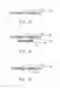
Referring to FIG. 1 onwards, process flowcharts of manufacturing an independent semiconductor package according to a first embodiment of the invention are shown. Firstly, a carrier 10 is provided. In the present embodiment of the invention, the carrier 10 is a steel piece. Then, referring to FIG. 2, a photo-resist layer 11 is formed on the carrier 10 first, and further shaped as a patterned photo-resist layer 11′ as indicated in FIG. 3.
Referring to FIG. 4, a conductive layer 20 is formed in the empty part of the photo-resist layer 11′, wherein the thickness of the conductive layer 20 normally between ranges 0.01˜0.4 mm, but preferably ranges between 0.025˜0.035 mm. In the present embodiment of the invention, the conductive layer 20 is formed by electroplating. As indicated in FIG. 5, the photo-resist layer 11′ is removed, but the conductive layer 20 (the first conductive layer) is left and used as package traces not the traces inside a semiconductor chip. In the present embodiment of the invention, a plurality of package traces formed by the conductive layer 20 are preferably electrically isolated and used as a package trace layout unit. In practical application, the package traces are electrically connected to each other. During the process of formation, a plurality of package trace layout units are formed, and each package trace layout unit substantially has the same pattern and individually corresponds to a to-be-packaged chip.
Referring to FIG. 6, a mold 23 is provided, wherein the mold 23 has a plurality of protrusions corresponding to the position of the trace layer 20. Then, an insulating material is infused to form a first insulating layer 21, wherein the thickness of the first insulating layer 21 normally ranges between 0.1˜0.4 mm, but preferably ranges between 0.18˜0.22 mm. As indicated in FIG. 7, a plurality of package traces are embedded in the first insulating layer 21 or disposed in the first insulating layer 21 and extended to a surface of the first insulating layer 21. In the present embodiment of the invention, the insulating material is a molding material, the elastic modulus of the insulating material is larger than 1.0 GPa, and preferably the CTE value of the insulating material is less than 10 ppm. In practical application, the first insulating layer 21 is not necessarily limited to one layer. Any one who is skilled in the technology of the invention can use several materials to compose a compound insulating layer in several times of formation or use the same material to compose an insulating layer in several times of formation, and such modifications are still within the scope of protection of the invention. However, in the present embodiment of the invention, the first insulating layer 21 is formed from a single material, such that the package traces are embedded in the first insulating layer 21. That is, the height of the first insulating layer 21 must be larger than the height of the package traces.
As a plurality of protrusions disposed on the mold 23 correspond to the trace layer 20, a plurality of holes 22 are formed on a surface of the first insulating layer 21. Referring to FIG. 8, the mold 23 and the carrier 10 are removed, and a semiconductor package that can be transported independently is formed. In the present embodiment of the invention, the other end of the holes 22 contacts the package trace of the trace layer 20, wherein the holes used as positioning units for connecting the conductors are made from the trace layer 20
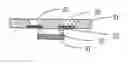
Referring to FIG. 9, an independent semiconductor package manufactured according to FIG. 8 is connected to a chip 31 via a second conductor. In the present embodiment of the invention, the second conductor is connected to the chip 31 via a solder 33 and a pillar bump 32. Besides, as indicated in FIG. 10, the hole 22 can be fully or partly filled with a conductive material, such as nickel, gold, copper or solder, to form a second conductive layer 41. In the present embodiment of the invention, the conductive material is formed by solder 41 to facilitate subsequent processing.
Referring to FIG. 11, the conductor 42 is fixed on the independent semiconductor package via position-setting of the holes 22, such that the signal of the chip 31 is transmitted externally via pillar bump 32, the solder 33, the trace layer 20, and the conductor 42. In the present embodiment of the invention, the conductor 42 is a solder ball or a trace and the conductor 42 could be used to connect to printed circuit board (PC Board) or another layer of receiving substrate. To avoid the solder of the solder ball flowing everywhere when melted, the positioning unit limits is for confining the solder to be within the hole 22. In the present embodiment of the invention, the positioning unit is a hole 22, which can be a run through hole or an indent only.
The solder 41 enables the electrically connection between the conductor 42 and the trace layer 20 even more tightly, and avoids the occurrence of bubbles which occurs when a solder ball is used as the conductor 42 but can not completely fill up the hole 22.
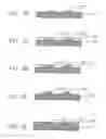
On the other hand, the independent semiconductor package and the package of the chip 31 can be flexible. Referring to FIG. 12, an insulating material, such as an encapsulating material, can be used as a second insulating layer 51 and infused to the chip 31 to encapsulate the pillar bump 32 but exposes the chip 31. Or, as indicated in FIG. 13, the second insulating layer 52 encapsulates the pillar bump 32 and the chip 31 but exposes the upper surface of the chip 31. Or, as indicated in FIG. 14, the second insulating layer 53 encapsulates the pillar bump 32 but is aligned with the chip 31.
Besides, the semiconductor package is also used in a multi-chip package. Referring to FIG. 15, a space 72 permitting the chip 61 to be fixed and connected to the trace is disposed in addition to the hole of the first insulating layer, and the chip is connected to the solder ball via a hole 22′.
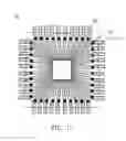
Referring to FIG. 16, a perspective of a lead frame according to a first embodiment of the invention is shown FIG. 16 is bottom view of FIG. 8, wherein the package trace layout unit 80 formed by a first conductive layer is embedded in the first insulating layer 21, and a plurality of fiducial marks 90 are used for positioning a lead frame when the chip is packaged. In the present embodiment of the invention, the shape of individual package trace layout unit 80 is indicated in FIG. 17. A package trace layout unit 80 comprises a plurality of electrically isolated package traces to form the pattern of a package trace layout unit and correspond to a to-be-packaged chip, wherein smaller chips are electrically connected via the conductive dots 84, and larger chips are electrically connected via the conductive dots 74. Thus, it can be used as the lead frame of different sized chips in the present embodiment of the invention. As indicated in FIG. 16 and FIG. 17, the package trace layout units 80 substantially have the same pattern, and the package trace layout units 80, isolated between each other, are arranged in a matrix and embedded in the first insulating layer 21.
Each package trace layout unit 80 preferably has a fan-in or fan-out pattern. The first conductive layer 20 and the second conductive layer 41 can have different pitches to achieve the function of fine pitch.
Second Embodiment
Referring to FIG. 18 and onwards, a method of manufacturing a semiconductor package according to a second embodiment of the invention is shown. Firstly, a carrier 19 is provided, wherein the carrier 19 is made from copper in the present embodiment of the invention. Like FIG. 1 to FIG. 4 of the first embodiment, other manufacturing methods obtain the stage result as indicated in FIG. 18, a patterned first conductive layer 20′ is formed on the carrier 19.
Referring to FIG. 19, a layer photo-resist layer 25 is coated on the first conductive layer 20′, and a hole 27′ is formed on the patterned photo-resist layer 25. Referring to FIG. 20, a second conductive layer 27 is formed in the hole 27′. In the present embodiment of the invention, the second conductive layer 27 is formed by way of electroplating and is substantially flat nor protruded from the surface of the first insulating layer 28.
The photo-resist layer 25 is removed such that a patterned first conductive layer 20′ and a second conductive layer 27 are obtained as indicated in FIG. 21. Referring to FIG. 22, a molding material is injected to form a first insulating layer 28, such that the patterned first conductive layer 20′ and the second conductive layer 27 are embedded in the first insulating layer 28. In the present embodiment of the invention, the molding material used to form the first insulating layer 28 is epoxy resin, the elastic modulus of the molding material is greater than 1.0 GPa, but the CTE value of the elastic modulus is less than 10 ppm.
By way of etching, the carrier 19 is removed to obtain a semiconductor package before package as indicated in FIG. 23. The application of the unpackaged semiconductor package is indicated in FIG. 24, and the unpackaged semiconductor package can be connected to the chip 31′ via the solder 33′, the pillar bump 32′.
Besides, the second conductive layer 27 can be pre-treated to resolve the resin residue problem arising in a QFN package when the tape is removed.
Referring to FIG. 25, a conductive protrusion 39 can be disposed on the first conductive layer 20′ of the package trace layout. The conductive protrusion 39 can be made from silver, gold, other metals or conductive materials, and the part of the package trace layout directly atop of the conductive protrusion is the molding material of the first insulating layer 28. Thus, when the unpackaged semiconductor package is used in conventional wiring bonding, the trace can be connected to the conductive protrusion 39 such that the lead frame neighbors the chip package as close as possible and will not wobble when connected to the traces, hence increasing the efficiency of bonding the wire to the chip.
Third Embodiment
Referring to FIG. 26 and onwards, a method of manufacturing a semiconductor package according to a third embodiment of the invention is shown. Firstly, a carrier 19′ is provided, wherein the carrier 19′ is made from copper in the present embodiment of the invention. Like FIG. 1 to FIG. 4 of the first embodiment, other manufacturing methods obtain the stage result as indicated in FIG. 26, a patterned first conductive layer 20′ is formed on the carrier 19′.
Referring to FIG. 27, a layer photo-resist layer 25 is coated on the first conductive layer 20′, and a hole 27′ is formed on the patterned photo-resist layer 25. Referring to FIG. 28, a second conductive layer 27 is formed in the hole 27′. In the present embodiment of the invention, the second conductive layer 27 is formed by way of electroplating and is substantially flat nor protruded from the surface of the first insulating layer 28.
The photo-resist layer 25 is removed such that a patterned first conductive layer 20′ and a second conductive layer 27 are obtained as indicated in FIG. 29. Referring to FIG. 30, a molding material is injected to form a first insulating layer 28, such that the patterned first conductive layer 20′ and the second conductive layer 27 are embedded in the first insulating layer 28. In the present embodiment of the invention, the molding material used to form the first insulating layer 28 is epoxy resin, the elastic modulus of the molding material is greater than 1.0 GPa, but the CTE value of the elastic modulus is less than 10 ppm.
By way of etching, part of the carrier 19′ is selectly removed to obtain a semiconductor package before package as indicated in FIGS. 31-35.
Referring to FIG. 31, a photo resist layer 81 is formed on the carrier 19′. Then the photo resist layer 81 is exposed via a mask 82 having at least a first opening 82a and at least a second opening 82b as shown in FIG. 32. And a patterned photo resist layer 81 having at least a first opening 81a and at least a second opening 81b is obtained as indicated in FIG. 33. Wherein the first opening 81a and the first opening 82a are corresponding with the inside area of the first insulating layer 28, and the second opening 81b and the second opening 82b are corresponding with the outside area of the first insulating layer 28.
Afterwards, referring to FIG. 34, the carrier 19′ is etched by taking the patterned photo resist layer 81 as a mask. Wherein the carrier 19′ and part of the first conductive layer 20′ are etched simultaneously so that the surface 20′a of the first conductive layer 20′ and the surface 28′a of the first insulating layer 28a are not located at the same plane. Then, the patterned photo resist layer 81 is removed so that an enforcement ring 19′c and at least a positioning hole 19′b are formed on the carrier 19′ as indicated in FIG. 35.
Please refer to FIG. 36. After part of the carrier 19′ is selectly removed, the enforcement ring 19′c is formed on the peripheral area of the carrier 19′ and the positioning hole 19′b are formed in the enforcement ring 19′c. The semiconductor package can be carried via the enforcement ring 19′c and the position hole 19′b without touching the first insulating layer 28 or the second conductive layer 27. Therefore, the scraping damage of the semiconductor package can be prevented.
The conductive layer 20 or 20′ (the package trace) is formed during the manufacturing process without applying extra process such as micro-filming, exposure and etching on the conductive layer, so that the conductive layer is not restricted by the etching pitch and the reliability of the package trace will not be affected by undercutting. However, the package trace meets the requirement of miniaturization in the semiconductor element better.
The package trace layout unit has a fan-in or fan-out pattern to achieve the function of fine pitch.
Moreover, the hole 22 (the positioning unit) makes the positioning setting of connecting the solder ball to the package element more precisely, and avoids the overflowing of the solder when melted.
Besides, the mold 23, and hole 22 (the positioning unit) are formed by using the material of the first insulating layer 21 directly, such that the first insulating layer 21 and the positioning unit are formed by one filling of the molding material, largely simplifying the manufacturing process of the semiconductor package.
Moreover, according to FIG. 11, with the disposition of the package trace 20, the pitch between the solder balls can be larger than the pitch between the chip bumps 32. Therefore, the technology of the invention can be applied to a manufacturing process with a lower requirement of the pitch.
Furthermore, the first insulating layer 21 uses a molding material as a carrier for the package trace pattern, therefore the package trace patterns are not connected by metallic traces and are different form conventional lead frame which has traces for connecting the package trace patterns. The insulating layer between the traces of the lead frame is simply used for insulating purpose and can not be used as a carrier. As a result, in the embodiments of the invention does not have the connecting traces for connecting the lead frame patterns, and each package has an individual pattern, and is easier for cutting.
In a conventional chip, the package traces are connected via metallic traces, therefore the package traces must be divided first before the chip can be tested individually. In the above embodiments, as each package trace pattern is electrically isolated and does not have metallic traces for connection, the chip still can be tested even after the chip is connected to the package trace, largely saving time and cost for testing.
While the invention has been described by way of example and in terms of a preferred embodiment, it is to be understood that the invention is not limited thereto. On the contrary, it is intended to cover various modifications and similar arrangements and procedures, and the scope of the appended claims therefore should be accorded the broadest interpretation so as to encompass all such modifications and similar arrangements and procedures. For examples, the first insulating layer 21, is not necessarily limited to one layer. Any one who is skilled in the technology of the invention can use several materials to compose a compound insulating layer in several times of formation or use the same material to compose an insulating layer in several times of formation, and such modifications are still within the scope of protection of the invention which is defined in the appended claims.
Claims
What is claimed is:1. A method of manufacturing a semiconductor package, comprising the following steps of:
providing a carrier;
forming a plurality of electrically isolated package trace layout units formed by a first conductive layer, wherein the package trace layout unit is formed by a plurality of electrically isolated package traces;
forming a patterned second conductive layer on the first conductive layer;
forming a first insulating layer formed by a molding material and embedded in the first conductive layer and the second conductive layer; and
selectively removing part of the carrier.
2. The manufacturing method of semiconductor package according to claim 1, wherein the step of selectively removing part of the carrier further comprises:
forming a photo resist layer on the carrier;
patterning the photo resist layer;
etching the carrier by taking the patterned photo resist layer as a mask; and
removing the patterned photo resist layer.
3. The manufacturing method of semiconductor package according to claim 2, wherein the step of etching the carrier further comprises:
etching the carrier and part of the first conductive layer simultaneously so that the surface of the first conductive layer and the surface of the first insulating layer are not located at the same plane.
4. The manufacturing method of semiconductor package according to claim 2, wherein the patterned photo resist layer has at least a first opening and at least a second opening, the first opening is corresponding with the inside area of the first insulating layer, and the second opening is corresponding with the outside area of the first insulating layer.
Images & Drawings included:


Sources:
- United States Patent and Trademark Office - verify current appl. status at the USPTO↗
Similar patent applications:
Recent applications in this class:
- » 20250293212 2025-09-18
SEMICONDUCTOR PACKAGES - » 20250293211 2025-09-18
HEAT DISSIPATION FOR STACKED INTEGRATED CIRCUIT DEVICES - » 20250293210 2025-09-18
SYSTEMS AND METHODS FOR PACKAGING A SEMICONDUCTOR DEVICE - » 20250286021 2025-09-11
SEMICONDUCTOR PACKAGE - » 20250286020 2025-09-11
SEMICONDUCTOR BONDING STRUCTURE - » 20250286019 2025-09-11
SEMICONDUCTOR PACKAGE - » 20250286018 2025-09-11
METHOD OF FABRICATING SEMICONDUCTOR BONDING STRUCTURE - » 20250286017 2025-09-11
SEMICONDUCTOR DEVICE - » 20250279399 2025-09-04
SEMICONDUCTOR DEVICES AND MANUFACTURING METHODS OF THE SAME - » 20250279398 2025-09-04
VERTICAL INTERCONNECT STRUCTURES IN THREE-DIMENSIONAL INTEGRATED CIRCUITS
Recent applications for this Assignee:
- » 20190035643 2019-01-31
Semiconductor structure and semiconductor package device using the same - » 20180323121 2018-11-08
Multi-layer substrate for semiconductor packaging - » 20170303399 2017-10-19
Manufacturing method of semiconductor package - » 20160329306 2016-11-10
SEMICONDUCTOR PACKAGE AND MANUFACTURING METHOD THEREOF - » 20160293416 2016-10-06
Manufacturing method of package substrate and package manufacturing method of semiconductor device - » 20160268225 2016-09-15
CHIP AND MANUFACTURING METHOD THEREOF - » 20160189981 2016-06-30
Manufacturing method of substrate structure having embedded interconnection layers - » 20160118349 2016-04-28
Semiconductor package - » 20160013139 2016-01-14
Semiconductor structure and method of fabricating the same - » 20150155214 2015-06-04
Multi-layer substrate for semiconductor packaging