Systems and methods to laminate passives onto substrate
US20080148560A1
2008-06-26
11/642,350
2006-12-20
✅ Patent granted
US 7,838,419 B2
2010-11-23
-
-
Thinh T Nguyen
2029-06-25
Abstract:
A method may include depositing a dielectric layer onto a substrate, removing portions of the dielectric layer to create a plurality of separated non-removed portions of the dielectric layer, depositing one or more passive electronic components into each of the plurality of separated non-removed portions, and curing the separated non-removed portions of the dielectric layer.
Inventors:
- Islam Salama 26 🇺🇸 Chandler, AZ, United States
- Islam A. Salama 53 🇺🇸 Chandler, AZ, United States
- Huankiat SEH 12 🇺🇸 Phoenix, AZ, United States
- Yongki MIN 52 🇺🇸 Phoenix, AZ, United States
Assignee:
- INTEL CORPORATION 47,158 🇺🇸 Santa Clara, CA, United States
Interested in similar patents?
Get notified when new applications in this technology area are published.
Classification:
H05K1/185 » CPC main
Printed circuits; Printed circuits structurally associated with non-printed electric components associated with components mounted in the printed circuit board, e.g. insert mounted components [IMC] Components encapsulated in the insulating substrate of the printed circuit or incorporated in internal layers of a multilayer circuit
H01L23/642 » CPC further
Details of semiconductor or other solid state devices; Structural electrical arrangements for semiconductor devices not otherwise provided for, e.g. in combination with batteries; Impedance arrangements Capacitive arrangements
H01L24/97 » CPC further
Arrangements for connecting or disconnecting semiconductor or solid-state bodies; Methods or apparatus related thereto; Batch processes at chip-level, i.e. with connecting carried out on a plurality of singulated devices, i.e. on diced chips the devices being connected to a common substrate, e.g. interposer, said common substrate being separable into individual assemblies after connecting
H01L25/50 » CPC further
Assemblies consisting of a plurality of individual semiconductor or other solid state devices ; Multistep manufacturing processes thereof Multistep manufacturing processes of assemblies consisting of devices, each device being of a type provided for in group or
H05K1/023 » CPC further
Printed circuits; Details; Electrical arrangements not otherwise provided for; Reduction of cross-talk, noise or electromagnetic interference using auxiliary mounted passive components or auxiliary substances
H05K1/023 » CPC further
Printed circuits; Details; Electrical arrangements not otherwise provided for; Reduction of cross-talk, noise or electromagnetic interference using auxiliary mounted passive components or auxiliary substances
H05K1/183 » CPC further
Printed circuits; Printed circuits structurally associated with non-printed electric components associated with components mounted in the printed circuit board, e.g. insert mounted components [IMC] Components mounted in and supported by recessed areas of the printed circuit board
H01L23/50 » CPC further
Details of semiconductor or other solid state devices; Arrangements for conducting electric current to or from the solid state body in operation, e.g. leads, terminal arrangements ; Selection of materials therefor for integrated circuit devices, e.g. power bus, number of leads
H01L2924/01005 » CPC further
Indexing scheme for arrangements or methods for connecting or disconnecting semiconductor or solid-state bodies as covered by; Chemical elements Boron [B]
H01L2924/01006 » CPC further
Indexing scheme for arrangements or methods for connecting or disconnecting semiconductor or solid-state bodies as covered by; Chemical elements Carbon [C]
H01L2924/01027 » CPC further
Indexing scheme for arrangements or methods for connecting or disconnecting semiconductor or solid-state bodies as covered by; Chemical elements Cobalt [Co]
H01L2924/01033 » CPC further
Indexing scheme for arrangements or methods for connecting or disconnecting semiconductor or solid-state bodies as covered by; Chemical elements Arsenic [As]
H01L2924/14 » CPC further
Indexing scheme for arrangements or methods for connecting or disconnecting semiconductor or solid-state bodies as covered by; Details of semiconductor or other solid state devices to be connected; Device type Integrated circuits
H01L2924/19041 » CPC further
Indexing scheme for arrangements or methods for connecting or disconnecting semiconductor or solid-state bodies as covered by; Details of hybrid assemblies other than the semiconductor or other solid state devices to be connected; Structure; Component type being a capacitor
H01L2924/19042 » CPC further
Indexing scheme for arrangements or methods for connecting or disconnecting semiconductor or solid-state bodies as covered by; Details of hybrid assemblies other than the semiconductor or other solid state devices to be connected; Structure; Component type being an inductor
H01L2924/19105 » CPC further
Indexing scheme for arrangements or methods for connecting or disconnecting semiconductor or solid-state bodies as covered by; Details of hybrid assemblies other than the semiconductor or other solid state devices to be connected; Disposition of discrete passive components in a side-by-side arrangement on a common die mounting substrate
H05K3/0032 » CPC further
Apparatus or processes for manufacturing printed circuits; Working of insulating substrates or insulating layers; Etching of the substrate by chemical or physical means by laser ablation of organic insulating material
H05K3/0032 » CPC further
Apparatus or processes for manufacturing printed circuits; Working of insulating substrates or insulating layers; Etching of the substrate by chemical or physical means by laser ablation of organic insulating material
H05K3/0052 » CPC further
Apparatus or processes for manufacturing printed circuits; Working of insulating substrates or insulating layers; Mechanical working of the substrate, e.g. drilling or punching Depaneling, i.e. dividing a panel into circuit boards; Working of the edges of circuit boards
H05K3/0052 » CPC further
Apparatus or processes for manufacturing printed circuits; Working of insulating substrates or insulating layers; Mechanical working of the substrate, e.g. drilling or punching Depaneling, i.e. dividing a panel into circuit boards; Working of the edges of circuit boards
H05K2201/09036 » CPC further
Indexing scheme relating to printed circuits covered by; Shape and layout; Substrate related Recesses or grooves in insulating substrate
H05K2201/09036 » CPC further
Indexing scheme relating to printed circuits covered by; Shape and layout; Substrate related Recesses or grooves in insulating substrate
H05K2201/0909 » CPC further
Indexing scheme relating to printed circuits covered by; Shape and layout; Substrate related Preformed cutting or breaking line
H05K2201/0909 » CPC further
Indexing scheme relating to printed circuits covered by; Shape and layout; Substrate related Preformed cutting or breaking line
H05K2201/10636 » CPC further
Indexing scheme relating to printed circuits covered by; Details of components or other objects attached to or integrated in a printed circuit board; Details of electrical connections of non-printed components, e.g. special leads; Components characterised by their electrical contacts Leadless chip, e.g. chip capacitor or resistor
Y02P70/50 » CPC further
Climate change mitigation technologies in the production process for final industrial or consumer products Manufacturing or production processes characterised by the final manufactured product
Y02P70/50 » CPC further
Climate change mitigation technologies in the production process for final industrial or consumer products Manufacturing or production processes characterised by the final manufactured product
Y10T29/49146 » CPC further
Metal working; Method of mechanical manufacture; Electrical device making; Conductor or circuit manufacturing; On flat or curved insulated base, e.g., printed circuit, etc.; Assembling to base an electrical component, e.g., capacitor, etc. with encapsulating, e.g., potting, etc.
H05K3/30 IPC
Apparatus or processes for manufacturing printed circuits Assembling printed circuits with electric components, e.g. with resistor
H05K3/30 IPC
Apparatus or processes for manufacturing printed circuits Assembling printed circuits with electric components, e.g. with resistor
H01L21/44 IPC
Processes or apparatus adapted for the manufacture or treatment of semiconductor or solid state devices or of parts thereof; Manufacture or treatment of semiconductor devices or of parts thereof the devices having at least one potential-jump barrier or surface barrier, e.g. PN junction, depletion layer or carrier concentration layer the devices having semiconductor bodies not provided for in groups, , , and with or without impurities, e.g. doping materials Manufacture of electrodes on semiconductor bodies using processes or apparatus not provided for in groups -
Description
BACKGROUND
Preformed passive electrical components may be embedded within an integrated circuit (IC) substrate in order to provide decoupling, RF tuning or voltage regulation. Such components must be electrically connected to conductive traces formed within the substrate.
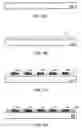
FIGS. 1A through 1D illustrate a conventional method to embed passive components within an IC substrate. Substrate 100 is shown at FIG. 1 and may comprise an organic substrate having any number of conductive and dielectric layers. Dielectric layer 110 is placed on substrate 100 as shown in FIG. 1B, and passive components 120 are placed into dielectric layer 110 at desired positions as shown in FIG. 1C. When located at the desired positions, passive components 120 are electrically connected to appropriate traces of substrate 100. Dielectric layer 110 is then cured, which causes layer 110 to shrink and components 120 to thereby move away from their desired positions. This movement may disconnect components 120 from appropriate conductive traces of substrate 100.
BRIEF DESCRIPTION OF THE DRAWINGS
FIGS. 1A through 1D illustrate fabrication of an apparatus.
FIG. 2 is a diagram of a process according to some embodiments.
FIGS. 3A through 3D illustrate some embodiments of the FIG. 2 process.
FIG. 4 is a diagram of a process according to some embodiments.
FIGS. 5A through 5D illustrate some embodiments of the FIG. 4 process.
FIG. 6 is a diagram of a process according to some embodiments.
FIGS. 7A through 7D illustrate some embodiments of the FIG. 6 process.
DETAILED DESCRIPTION
FIG. 2 is a diagram of process 200 to fabricate an apparatus according to some embodiments. Process 200 and each other process described herein may be executed by one or more fabrication devices, and all or a part of these processes may be executed manually. These processes 200 may be executed by an entity different from an entity that manufactures an IC die to which the fabricated apparatus is subsequently coupled.
A dielectric layer is initially deposited on a substrate at 210. The substrate may comprise any ceramic, organic, and/or other suitable material. The substrate may comprise any portion of an IC package substrate, including but not limited to a core, metallization layers and/or other dielectric layers. Accordingly, the dielectric layer may be deposited upon any suitable layer of a substrate at 210.
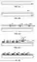
FIGS. 3A and 3B are side cross-sectional views showing substrate 300 and dielectric layer 310 deposited on substrate 300, respectively. Substrate 300 may be composed of any suitable material, including but not limited to bismalemide triazine (BT) and FR4. According to some embodiments, substrate 300 (and any other substrate referred to herein) may comprise a core layer with any number of build-up layers attached thereto. The build-up layers may comprise dielectric material and conductive interconnect traces. Dielectric layer 310 may comprise any suitable dielectric and may be deposited in any manner that is or becomes known. In some embodiments, dielectric layer 310 comprises B-stage Ajinomoto Build-up Film. Dielectric layer 310 may be uncured or partially cured prior to being deposited on substrate 300 according to some embodiments. Substrate 300 and dielectric layer 310 may be panel-sized and may therefore include elements of multiple IC package substrates.
Next, at 220, portions of the dielectric layer are removed to create a plurality of separated non-removed portions of the dielectric layer. FIG. 3C illustrates 220 according to some embodiments. Specifically, laser drill 320 directs laser beam 330 toward appropriate locations of dielectric layer 310 in order to laser-scribe a plurality of separated non-removed portions 340. Laser scribing as shown removes portions of dielectric layer 310 that reside between non-removed portions 340. Laser drill 320 may comprise a conventional tool for creating substrate vias.
One or more passive electronic components are then deposited into each of the non-removed portions at 230. Any system to deposit the components may be utilized at 230, including but not limited to surface mounter 350 of FIG. 3D. Passive components 360 may comprise any suitable electrical component, such as a capacitor or an inductor. Components 360 may be deposited at 230 in alignment with conductive traces of substrate 300 to which components 360 are intended to be coupled.
Next, at 240, the separated non-removed portions of the dielectric layer are cured. FIG. 3E illustrates cured separated non-removed portions 340 of dielectric layer 310. According to some embodiments, curing separated non-removed portions 340 results in less movement of components 360 than exhibited by prior systems. In this regard, some remnants of dielectric layer 310 may remain between the plurality of separated non-removed portions after 220, but the remnants do not substantially affect the shrinkage of adjacent non-removed portions.
Subsequent processing may include depositing a next dielectric layer onto dielectric layer 310, via formation, and/or patterning. Substrate 300 may be singulated to separate each non-removed portion into individual IC package substrates.
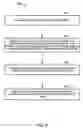
Process 400 of FIG. 4 also initially involves depositing a dielectric layer on a substrate. The substrate and the dielectric may comprise any of the implementations described with respect to process 200. FIGS. 5A and 5B depict deposition of the dielectric layer onto a substrate at 410 according to some embodiments.
A plurality of portions of the dielectric layer are cured at 420. The plurality of portions are separated by a plurality of non-cured portions. FIG. 5C illustrates curing according to some embodiments of 420. As shown, energy 520 is directed to portions of dielectric layer 510 using mask 530. Energy 520 may be delivered by any energy source suitable for curing dielectric layer 510, including but not limited to a laser, ultraviolet light, microwaves, etc. FIG. 5D shows uncured portions 540 of dielectric layer 510.
One or more passive electronic components are then deposited into each of the uncured portions at 430. Although any system may deposit the components at 430, FIG. 5D illustrates the use of surface mounter 550 to deposit components 560. Uncured portions 540 are then cured at 440. Since any one contiguous uncured portion may be smaller than that shown in FIG. 1C, components 560 may experience less movement during curing than in prior systems. Again, any suitable additional processing may be performed after 440.
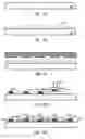
FIG. 6 illustrates process 600 according to some embodiments. A dielectric layer is deposited on a substrate at 610, as illustrated in FIGS. 7A and 7B. The dielectric layer is modified at 620 to create a plurality of mounting potions. The plurality of mounting portions are separated by a plurality of non-mounting portions which extend higher above the substrate than the mounting portions.
FIGS. 7C and 7D illustrate modification of dielectric layer 710 at 620 according to some embodiments. As shown, tool 720 is biased against dielectric layer 720 in order to compress mounting portions 730 located between non-mounting portions 740. In some embodiments, dielectric layer 710 is molded to create the structure illustrated in FIG. 7D.
One or more passive electronic components are then deposited into each of the plurality of mounting portions at 630. FIG. 7D shows surface mounter 750 depositing components 760 onto mounting portions 730. The entire dielectric layer, consisting of the plurality of mounting portions and the plurality of non-mounting portions, is then cured at 640. According to some embodiments, such as the FIG. 7E embodiment, the low profile of the plurality of mounting portions 730 with respect to the plurality of non-mounting portions 740 results in less movement of components 760 due to curing of dielectric layer 710.
The several embodiments described herein are solely for the purpose of illustration. The various features described herein need not all be used together, and any one or more of those features may be incorporated in a single embodiment. Some embodiments may include any currently or hereafter-known versions of the elements described herein. Therefore, persons skilled in the art will recognize from this description that other embodiments may be practiced with various modifications and alterations.
Claims
What is claimed is:1. A method comprising:
depositing a dielectric layer onto a substrate;
removing portions of the dielectric layer to create a plurality of separated non-removed portions of the dielectric layer;
depositing one or more passive electronic components into each of the plurality of separated non-removed portions; and
curing the separated non-removed portions of the dielectric layer.
2. A method according to claim 1, wherein removing the portions comprises:
laser scribing the plurality of separated non-removed portions.
3. A method according to claim 1, further comprising:
singulating the substrate,
wherein the substrate comprises a panel comprising a plurality of integrated circuit dice.
4. A method according to claim 1, further comprising:
depositing a second dielectric layer onto the dielectric layer.
5. A method according to claim 1, wherein the dielectric layer is partially cured before being deposited on the substrate.
6. A method comprising:
depositing a dielectric layer onto a substrate;
curing a plurality of portions of the dielectric layer, the plurality of cured portions separated by a plurality of uncured portions of the dielectric layer;
depositing one or more passive electronic components into respective ones of each of the plurality of uncured portions; and
curing the uncured portions of the dielectric layer.
7. A method according to claim 6, wherein curing the plurality of portions of the dielectric layer comprises:
exposing the plurality of portions to energy to which the plurality of uncured portions is not exposed.
8. A method according to claim 6, further comprising:
singulating the substrate,
wherein the substrate comprises a panel comprising a plurality of integrated circuit dice.
9. A method according to claim 6, further comprising:
depositing a second dielectric layer onto the dielectric layer.
10. A method according to claim 6, wherein the dielectric layer is partially cured before being deposited on the substrate.
11. A method comprising:
depositing a dielectric layer onto a substrate;
modifying the dielectric layer to create a plurality of mounting portions separated by a plurality of non-mounting portions, the non-mounting portions extending higher above the substrate than the mounting portions;
depositing one or more passive electronic components onto each of the plurality of mounting portions; and
curing the plurality of mounting portions and the plurality of non-mounting portions of the dielectric layer.
12. A method according to claim 11, wherein modifying the dielectric layer to create a plurality of mounting portions comprises:
compressing the plurality of non-mounting portions.
13. A method according to claim 11, further comprising:
singulating the substrate,
wherein the substrate comprises a panel comprising a plurality of integrated circuit dice.
14. A method according to claim 11, further comprising:
depositing a second dielectric layer onto the dielectric layer.
15. A method according to claim 11, wherein the dielectric layer is partially cured before being deposited on the substrate.
Images & Drawings included:


Sources:
- United States Patent and Trademark Office - verify current appl. status at the USPTO↗
Similar patent applications:
Recent applications in this class:
- » 20250294684 2025-09-18
PRINTED CIRCUIT BOARD WITH MOLD ADHESION BOUNDARY FOR DIE ATTACH PAD - » 20250267795 2025-08-21
Component Carrier With Constricted Through Hole and Electrically Insulating Coating - » 20250261314 2025-08-14
SUBSTRATE WITH BUILT-IN ELECTRONIC COMPONENTS - » 20250227851 2025-07-10
SUBSTRATE SUPPORT WITH PRINTED HEATER - » 20250220818 2025-07-03
FLOW ENHANCED DUMMY STRUCTURE TO ENABLE CAPILLARY FLOW BASED SIDEWALL FILLING - » 20250212336 2025-06-26
PRINTED CIRCUIT BOARD - » 20250212335 2025-06-26
PRINTED CIRCUIT BOARD - » 20250203782 2025-06-19
ELECTRONIC COMPONENT AND METHOD FOR MANUFACTURING SAME - » 20250203781 2025-06-19
RADIO FREQUENCY MODULE AND METHOD FOR MANUFACTURING THE SAME - » 20250168987 2025-05-22
MOLDED PACKAGES WITH THROUGH-MOLD INTERCONNECTS
Recent applications for this Assignee:
- » 20250294866 2025-09-18
GATE CUT CONFINED WITHIN GATE TRENCH - » 20250294846 2025-09-18
BACKSIDE CROSS-COUPLE INTERCONNECTS - » 20250294835 2025-09-18
ELONGATED VERTICAL STRUCTURES OF CHANNEL MATERIALS - » 20250294827 2025-09-18
CO-INTEGRATION OF GATE-ALL-AROUND DEVICES WITH DIFFERENT NUMBERS OF NANORIBBONS - » 20250294818 2025-09-18
TRANSISTOR DESIGNS FOR FLOATING BODY MEMORY - » 20250294781 2025-09-18
MAGNETIC CORE INDUCTORS ON PACKAGE SUBSTRATES - » 20250294777 2025-09-18
INTEGRATED CIRCUIT DEVICE WITH MEMORY ARRAY AND SHARED GAIN ELEMENT - » 20250293985 2025-09-18
RECEIVER-BASED PRECISION CONGESTION CONTROL - » 20250293860 2025-09-18
PRESERVATION OF CONFIDENTIALITY AND INTEGRITY OF MODELS DURING EXECUTION - » 20250293706 2025-09-18
LOW-RANK DECOMPOSITION-BASED HARDWARE COMPRESSION OF MATRICES AND TENSORS