Clustered stacked vias for reliable electronic substrates
US20090189290A1
2009-07-30
12/020,565
2008-01-27
✅ Patent granted
US 8,242,593 B2
2012-08-14
-
-
Shouxiang Hu
2029-07-10
Abstract:
A substrate via structure for stacked vias in a substrate/chip assembly includes: a center via stack and a plurality of stacked vias clustered around the center via stack. In this structure, the center via and the surrounding vias are made of copper. Some of the surrounding vias may be non-functional vias and these may be of a different height than the functional vias.
Inventors:
- Douglas O. Powell 25 🇺🇸 Endicott, NY, United States
- David L. Questad 50 🇺🇸 Hopewell Junction, NY, United States
- Sri M. Sri-Jayantha 98 🇺🇸 Ossining, NY, United States
- David J. Russell 35 🇺🇸 Owego, NY, United States
- Karan Kacker 9 🇺🇸 Atlanta, GA, United States
Assignee:
- INTERNATIONAL BUSINESS MACHINES CORPORATION 136,239 🇺🇸 ARMONK, NY, United States
Interested in similar patents?
Get notified when new applications in this technology area are published.
Classification:
H01L29/40 IPC
Semiconductor devices adapted for rectifying, amplifying, oscillating or switching, or capacitors or resistors with at least one potential-jump barrier or surface barrier, e.g. PN junction depletion layer or carrier concentration layer; Details of semiconductor bodies or of electrodes thereof; Multistep manufacturing processes therefor Electrodes ; Multistep manufacturing processes therefor
H01L23/49827 » CPC main
Details of semiconductor or other solid state devices; Arrangements for conducting electric current to or from the solid state body in operation, e.g. leads, terminal arrangements ; Selection of materials therefor consisting of soldered constructions; Leads, on insulating substrates, Via connections through the substrates, e.g. pins going through the substrate, coaxial cables
H01L23/498 » CPC further
Details of semiconductor or other solid state devices; Arrangements for conducting electric current to or from the solid state body in operation, e.g. leads, terminal arrangements ; Selection of materials therefor consisting of soldered constructions Leads, on insulating substrates,
H01L23/49838 » CPC further
Details of semiconductor or other solid state devices; Arrangements for conducting electric current to or from the solid state body in operation, e.g. leads, terminal arrangements ; Selection of materials therefor consisting of soldered constructions; Leads, on insulating substrates, Geometry or layout
H05K1/115 » CPC further
Printed circuits; Details; Printed elements for providing electric connections to or between printed circuits Via connections; Lands around holes or via connections
H05K1/115 » CPC further
Printed circuits; Details; Printed elements for providing electric connections to or between printed circuits Via connections; Lands around holes or via connections
H01L2224/05001 » CPC further
Indexing scheme for arrangements for connecting or disconnecting semiconductor or solid-state bodies and methods related thereto as covered by; Means for bonding being attached to, or being formed on, the surface to be connected, e.g. chip-to-package, die-attach, "first-level" interconnects; Manufacturing methods related thereto; Bonding areas; Manufacturing methods related thereto; Structure, shape, material or disposition of the bonding areas prior to the connecting process of an individual bonding area Internal layers
H01L2224/16 » CPC further
Indexing scheme for arrangements for connecting or disconnecting semiconductor or solid-state bodies and methods related thereto as covered by; Means for bonding being attached to, or being formed on, the surface to be connected, e.g. chip-to-package, die-attach, "first-level" interconnects; Manufacturing methods related thereto; Bump connectors; Manufacturing methods related thereto; Structure, shape, material or disposition of the bump connectors after the connecting process of an individual bump connector
H01L2924/01078 » CPC further
Indexing scheme for arrangements or methods for connecting or disconnecting semiconductor or solid-state bodies as covered by; Chemical elements Platinum [Pt]
H01L2924/10253 » CPC further
Indexing scheme for arrangements or methods for connecting or disconnecting semiconductor or solid-state bodies as covered by; Details of semiconductor or other solid state devices to be connected; Material of the semiconductor or solid state bodies; Semiconducting materials; Elemental semiconductors, i.e. Group IV Silicon [Si]
H01L2924/15151 » CPC further
Indexing scheme for arrangements or methods for connecting or disconnecting semiconductor or solid-state bodies as covered by; Details of package parts other than the semiconductor or other solid state devices to be connected; Die mounting substrate; Shape the die mounting substrate comprising an aperture, e.g. for underfilling, outgassing, window type wire connections
H01L2924/15311 » CPC further
Indexing scheme for arrangements or methods for connecting or disconnecting semiconductor or solid-state bodies as covered by; Details of package parts other than the semiconductor or other solid state devices to be connected; Die mounting substrate; Connection portion the connection portion being formed only on the surface of the substrate opposite to the die mounting surface being a ball array, e.g. BGA
H05K1/0222 » CPC further
Printed circuits; Details; Electrical arrangements not otherwise provided for; Reduction of cross-talk, noise or electromagnetic interference by printed shielding conductors, ground planes or power plane; Printed shielding conductors for shielding around or between signal conductors, e.g. coplanar or coaxial printed shielding conductors for shielding around a single via or around a group of vias, e.g. coaxial vias or vias surrounded by a grounded via fence
H05K3/4602 » CPC further
Apparatus or processes for manufacturing printed circuits; Manufacturing multilayer circuits characterized by a special circuit board as base or central core whereon additional circuit layers are built or additional circuit boards are laminated
H05K3/4602 » CPC further
Apparatus or processes for manufacturing printed circuits; Manufacturing multilayer circuits characterized by a special circuit board as base or central core whereon additional circuit layers are built or additional circuit boards are laminated
H05K2201/096 » CPC further
Indexing scheme relating to printed circuits covered by; Shape and layout; Shape and layout details of conductors; Conductive through-holes or vias Vertically aligned vias, holes or stacked vias
H05K2201/096 » CPC further
Indexing scheme relating to printed circuits covered by; Shape and layout; Shape and layout details of conductors; Conductive through-holes or vias Vertically aligned vias, holes or stacked vias
H05K2201/09609 » CPC further
Indexing scheme relating to printed circuits covered by; Shape and layout; Shape and layout details of conductors; Conductive through-holes or vias Via grid, i.e. two-dimensional array of vias or holes in a single plane
H05K2201/09609 » CPC further
Indexing scheme relating to printed circuits covered by; Shape and layout; Shape and layout details of conductors; Conductive through-holes or vias Via grid, i.e. two-dimensional array of vias or holes in a single plane
Y10T29/49155 » CPC further
Metal working; Method of mechanical manufacture; Electrical device making; Conductor or circuit manufacturing; On flat or curved insulated base, e.g., printed circuit, etc. Manufacturing circuit on or in base
Y10T29/49165 » CPC further
Metal working; Method of mechanical manufacture; Electrical device making; Conductor or circuit manufacturing; On flat or curved insulated base, e.g., printed circuit, etc.; Manufacturing circuit on or in base by forming conductive walled aperture in base
Y10T29/49204 » CPC further
Metal working; Method of mechanical manufacture; Electrical device making; Conductor or circuit manufacturing Contact or terminal manufacturing
Y10T29/49222 » CPC further
Metal working; Method of mechanical manufacture; Electrical device making; Conductor or circuit manufacturing; Contact or terminal manufacturing by assembling plural parts forming array of contacts or terminals
H01L2224/05599 » CPC further
Indexing scheme for arrangements for connecting or disconnecting semiconductor or solid-state bodies and methods related thereto as covered by; Means for bonding being attached to, or being formed on, the surface to be connected, e.g. chip-to-package, die-attach, "first-level" interconnects; Manufacturing methods related thereto; Bonding areas; Manufacturing methods related thereto; Structure, shape, material or disposition of the bonding areas prior to the connecting process of an individual bonding area; External layer Material
H01L2924/00014 » CPC further
Indexing scheme for arrangements or methods for connecting or disconnecting semiconductor or solid-state bodies as covered by; Technical content checked by a classifier the subject-matter covered by the group, the symbol of which is combined with the symbol of this group, being disclosed without further technical details
H01L2224/05099 » CPC further
Indexing scheme for arrangements for connecting or disconnecting semiconductor or solid-state bodies and methods related thereto as covered by; Means for bonding being attached to, or being formed on, the surface to be connected, e.g. chip-to-package, die-attach, "first-level" interconnects; Manufacturing methods related thereto; Bonding areas; Manufacturing methods related thereto; Structure, shape, material or disposition of the bonding areas prior to the connecting process of an individual bonding area; Internal layers Material
H01L21/00 IPC
Processes or apparatus adapted for the manufacture or treatment of semiconductor or solid state devices or of parts thereof
H01L23/04 IPC
Details of semiconductor or other solid state devices; Containers; Seals characterised by the shape of the container or parts, e.g. caps, walls
H01L23/48 IPC
Details of semiconductor or other solid state devices Arrangements for conducting electric current to or from the solid state body in operation, e.g. leads, terminal arrangements ; Selection of materials therefor
H01L23/52 IPC
Details of semiconductor or other solid state devices Arrangements for conducting electric current within the device in operation from one component to another, i.e. interconnections, e.g. wires, lead frames
Description
CROSS-REFERENCE TO RELATED APPLICATIONS
A via system designed to reduce Z-axis strain has been disclosed in commonly-owned, co-pending U.S. patent application Ser. No. 12/020,534, “Construction Of Reliable Stacked Via In Electronic Substrates—Vertical Stiffness Control Method,” filed on Jan. 26, 2008, Attorney Docket Number YOR920060720US1. An embedded constrainer disc system around a stack via to reduce the in-plane strain has also been disclosed in commonly-owned, co-pending U.S. patent application Ser. No. 12/020,561, “Embedded Constrainer Discs For Reliable Stacked Vias In Electronic Substrates,” filed on Jan. 27, 2008, Attorney Docket Number YOR920060721US1.
STATEMENT REGARDING FEDERALLY SPONSORED-RESEARCH OR DEVELOPMENT
None.
INCORPORATION BY REFERENCE OF MATERIAL SUBMITTED ON A COMPACT DISC
None.
FIELD OF THE INVENTION
The invention disclosed broadly relates to the field of manufacturing electronic substrates and more particularly relates to the field of stacked vias on electronic substrates.
BACKGROUND OF THE INVENTION
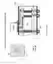
FIG. 1 shows two key components of an electronic module. A chip 100 is made of silicon on which electronic circuits are fabricated. A substrate 102 is made of organic materials embedded with copper interconnects. A substrate 102 facilitates electrical interconnection of the chip to external electronic circuits on a motherboard.
The density of connection points (controlled collapse chip connection, or “C4s”) between a chip 100 and a substrate 102 is a critical parameter. A larger number of C4s requires multiple build-up layers 104 to achieve the needed electrical connections to the motherboard. A typical substrate 102 may have four build-up layers 104 on top and bottom and support about 3,000 C4s. FIG. 1 shows stacked vias 106 as well as staggered vias 108 needed to complete the interconnection. Stacked vias 106 are often preferable because they achieve a C4 connection density upwards of 20% as compared to a staggered via 108.
FIG. 2 shows the known art with regard to a stacked via 206 and a plated through hole 210 (PTH). An individual stacked via 206 as shown in FIG. 2 accumulates various levels of strain as it is thermally cycled. In a planar view the stacked vias 206 are located wherever it is convenient to embed them by the electrical designer of a substrate. The coefficient of thermal expansion (CTE) of various materials used to construct a module is not matched and is known to drive thermomechanical stresses within a module. Repeated thermal cycling of an electronic module exhibits failure at via interface regions due to thermomechanically driven accumulated strain. An individual via stack 206 is strained along the Z-axis as well as the (X-Y) plane by the CTE-driven thermo-mechanical stresses.
SUMMARY OF THE INVENTION
Briefly, according to an embodiment of the invention, a method for creating a clustered via structure includes steps or acts of: creating a center via stack for electrical interconnects in a substrate/chip assembly; and adding additional via stacks surrounding the center via stack. Some of the additional via stacks may be non-functional and may be of a different height than the functional via stacks.
A substrate via structure for stacked vias in a substrate/chip assembly includes: a center via stack and a plurality of stacked vias clustered around the center via stack. In this structure, the center via and the surrounding vias are made of copper. Some of the surrounding vias may be non-functional vias and these may be of a different height than the functional vias.
BRIEF DESCRIPTION OF THE DRAWINGS
To describe the foregoing and other exemplary purposes, aspects, and advantages, we use the following detailed description of an exemplary embodiment of the invention with reference to the drawings, in which:
FIG. 1 shows a basic electronic module, according to the known art;
FIG. 2 shows the stacked via of an electronic module, according to the known art;
FIG. 3A shows isolated vias, according to the known art;
FIG. 3B shows clustered vias, according to an embodiment of the present invention; and
FIG. 4 shows a clustered via analysis, according to an embodiment of the present invention.
FIG. 5 is a flow chart of a method for clustering stacked vias, according to an embodiment of the present invention.
While the invention as claimed can be modified into alternative forms, specific embodiments thereof are shown by way of example in the drawings and will herein be described in detail. It should be understood, however, that the drawings and detailed description thereto are not intended to limit the invention to the particular form disclosed, but on the contrary, the intention is to cover all modifications, equivalents and alternatives falling within the scope of the present invention.
DETAILED DESCRIPTION
We describe a via structure design for reducing strain on individual via stacks. Referring now in specific detail to the drawings, and particularly FIG. 3, there is illustrated a via stack design according to an embodiment of the present invention. FIG. 3 shows a design that reduces the effective strain on an individual via stack by actively clustering a group of vias 350. During a thermal cycle (e.g., 125 degC to −55 degC) as the build-up layers (with a CTE˜30 ppm/degC) shrink along the Z axis as well as in-plane (X-Y) much faster than the Cu-via (with a CTE˜16), an individual stacked via 340 has to single-handedly resist the thermomechanical forces produced by the surrounding build-up layer.
By clustering several stacked vias 350 together and by avoiding an isolated via 340, the load-carrying capacity of the clustered via 350 is enhanced without excessive plastic strain. It is known that the life-time of a via is non-linearly dependent on its plastic strain. Elastic strain in a material is reversible, whereas a plastic strain is irreversible. When the applied stress is removed an elastic deformation reverts back to its original shape whereas a plastic strain does not. Plastic strain, when produced repeatedly due to thermal cycling, is known to generate fatigue failure in materials. Thus it is important to minimize the plastic strains encountered by critical components within an electronic assembly.
Clustering of vias produces united resistance along the Z-axis as well as in the X-Y plane simultaneously. In essence, by increasing the copper content in relation to the build-up layer material, the clustered via stack 350 is better protected from plastic deformation.
Referring to FIG. 5 there is shown a flow chart of the process for creating clustered via stacks. In step 510, the center via is positioned. The location of the center via is kept constant with respect to a substrate/chip assembly. In step 520 additional vias are progressively added (1, 2 and so on.) on opposite sides of the center via. The following cumulative strain per deep thermal cycle (DTC) can be observed:
Base-line data with central via=0.7459%
Central via plus one on each side=0.7399%
Central via plus two on each side=0.7408%
The analysis shows that a single encirclement of an isolated via 340 produces an improved tolerance (i.e., a reduced strain). Adding an extra encirclement does not produce commensurate improvement. A three-dimensional (3D) formulation produces a similar trend as that of a two-dimensional (2D) model but the relative difference in strains between configurations typically is emphasized more.
While clustering vias for reducing strain, it may be possible to introduce surrounding via stacks that are not required by the electrical circuits. In step 430, the surrounding via stacks may have a different (smaller) total height compared to a functional via in order to be accommodated in a constrained surrounding. A constrained surrounding may have circuit interconnects on a top layer thus preventing a full height stack via.
As has been shown, there is an advantage in clustering a group of stacked vias in the design of an organic substrate even though it forces the designer to avoid isolated stacked vias 340.
Therefore, while there has been described what is presently considered to be the preferred embodiment, it is understood by those skilled in the art that other modifications can be made within the spirit of the invention.
Claims
1. A substrate via structure for stacked vias in a substrate/chip assembly, the structure comprising:
a center via stack; and
a plurality of stacked vias clustered around the center via stack.
2. The structure of claim 1 wherein the stacked vias are copper vias.
3. The structure of claim 1 wherein the center via stack comprises copper vias.
4. The structure of claim 1 comprising one stacked via on each side of the center via stack.
5. The structure of claim 1 comprising two stacked vias on each side of the center via stack.
6. The structure of claim 1 comprising three stacked vias on each side of the center via stack.
7. The structure of claim 1 comprising seven stacked vias surrounding the center via stack.
8. The structure of claim 8 further comprising additional stacked vias surrounding the center via stack.
9. The structure of claim 1 wherein a position of the center via stack is kept constant with respect to the substrate/chip assembly.
10. The structure of claim 9 wherein the plurality of stacked vias clustered around the center via stack comprise functional and non-functional vias, wherein non-functional vias are those that are not required for electrical interconnects.
11. The structure of claim 10 wherein the non-functional vias are of a different height than the functional vias.
12. The structure of claim 11 wherein the non-functional vias have different heights.
13. A method of creating a substrate via structure in a substrate/chip assembly, the method comprising steps of:
creating a center via stack for electrical interconnects in the substrate/chip assembly; and
adding additional via stacks surrounding the center via stack.
14. The method of claim 13 wherein the creating step comprises creating a copper center via stack.
15. The method of claim 14 wherein the additional via stacks comprise copper vias.
16. The method of claim 13 wherein the adding step comprises:
adding one additional via stack on each side of the center via stack.
17. The method of claim 16 wherein the adding step further comprises:
adding additional via stacks surrounding the center via stack.
18. The method of claim 13 wherein a position of the center via stack is kept constant with respect to the substrate/chip assembly.
19. The method of claim 18 wherein the adding step comprises adding non-functional vias, wherein non-functional vias are not required for facilitating electrical connections.
20. The method of claim 19 wherein the non-functional vias are of a different height than functional vias in order to accommodate a constrained surrounding area.
Images & Drawings included:


Sources:
- United States Patent and Trademark Office - verify current appl. status at the USPTO↗
Similar patent applications:
Recent applications in this class:
- » 20250293133 2025-09-18
Through Package Vertical Interconnect and Method of Making Same - » 20250293132 2025-09-18
CHIP PACKAGING METHOD AND CHIP PACKAGING STRUCTURE - » 20250285956 2025-09-11
PACKAGE STRUCTURE INCLUDING INACTIVE ELEMENT, ASSEMBLY STRUCTURE AND METHOD OF MANUFACTURING THE SAME - » 20250285955 2025-09-11
PACKAGE STRUCTURE INCLUDING INACTIVE ELEMENT, ASSEMBLY STRUCTURE AND METHOD OF MANUFACTURING THE SAME - » 20250285954 2025-09-11
PACKAGE STRUCTURE INCLUDING INACTIVE ELEMENT, ASSEMBLY STRUCTURE AND METHOD OF MANUFACTURING THE SAME - » 20250279343 2025-09-04
CERAMIC SUBSTRATE, METHOD FOR MANUFACTURING CERAMIC SUBSTRATE, LIGHT-EMITTING DEVICE, AND METHOD FOR MANUFACTURING LIGHT-EMITTING DEVICE - » 20250279342 2025-09-04
METAL SEED LAYERS WITH DIFFERENT SHEET RESISTANCES IN INTEGRATED CIRCUIT PACKAGES - » 20250273553 2025-08-28
2.5D/3D SYSTEM INTEGRATION - » 20250273552 2025-08-28
Semiconductor Device and Method of Forming Encapsulated Vertical Interconnect Structure - » 20250266341 2025-08-21
SEMICONDUCTOR SUBSTRATE STRUCTURE WITH MICROCHANNEL PLATE-BASED VIAS AND METHOD FOR MANUFACTURING THE SAME
Recent applications for this Assignee:
- » 20250294045 2025-09-18
THREAT POLICY FINE-TUNING BASED ON THE VULNERABILITY OF A SUBNET AS A SOURCE OF A MALICIOUS ATTACK - » 20250294041 2025-09-18
DEVICE POPULATION ANOMALY DETECTION - » 20250292574 2025-09-18
SCENE PARSING - » 20250292026 2025-09-18
A GENERATIVE ARTIFICIAL INTELLIGENCE COMMENTARY - » 20250291689 2025-09-18
MACHINE LEARNING MODEL TRAINING TO ASSIST IN SYSTEM DEBUG - » 20250287215 2025-09-11
PORTABLE MEDIA GEOFENCE AND DEVICE PAIRING SECURITY - » 20250285610 2025-09-11
RECIPIENT-SPECIFIC VOICE TONE ADJUSTMENT IN TELEPHONY - » 20250284728 2025-09-11
CONTEXT LARGE LANGUAGE MODEL OUTPUT EXPLANATION - » 20250278669 2025-09-04
COUNTERFACTUALS WITH FEATURE PREFERENCES FOR CONSISTENT AND DIVERSE EXPLANATIONS - » 20250274345 2025-08-28
MULTI-LAYER EDGE ARCHITECTURE SIMULATION