Method for forming an etched recess package on package system
US20100025830A1
2010-02-04
12/185,058
2008-08-01
✅ Patent granted
US 7,932,130 B2
2011-04-26
-
-
Zandra V. Smith | Khanh B Duong
2028-08-01
Abstract:
An integrated circuit package system includes: providing a die attach paddle with interconnection pads connected to a bottom surface of the die attach paddle; connecting a first device to the interconnection pads with a bond wire; connecting a lead to the interconnection pad or to the first device; encapsulating the first device and the die attach paddle with an encapsulation having a top surface; and etching the die attach paddle leaving a recess in the top surface of the encapsulation.
Inventors:
- Zigmund Ramirez Camacho 172 🇸🇬 Singapore, Singapore
- Henry Descalzo Bathan 108 🇸🇬 Singapore, Singapore
- Lionel Chien Hui Tay 116 🇸🇬 Singapore, Singapore
- Jairus Legaspi Pisigan 32 🇸🇬 Singapore, Singapore
Assignee:
- STATS CHIPPAC, LTD. 1,631 🇸🇬 Singapore, Singapore
Interested in similar patents?
Get notified when new applications in this technology area are published.
Classification:
H01L21/50 IPC
Processes or apparatus adapted for the manufacture or treatment of semiconductor or solid state devices or of parts thereof; Manufacture or treatment of semiconductor devices or of parts thereof the devices having at least one potential-jump barrier or surface barrier, e.g. PN junction, depletion layer or carrier concentration layer Assembly of semiconductor devices using processes or apparatus not provided for in a single one of the subgroups - , e.g. sealing of a cap to a base of a container
H01L23/49551 » CPC main
Details of semiconductor or other solid state devices; Arrangements for conducting electric current to or from the solid state body in operation, e.g. leads, terminal arrangements ; Selection of materials therefor consisting of soldered constructions; Lead-frames or other flat leads; Geometry of the lead-frame; Cross section geometry characterised by bent parts
H01L21/4828 » CPC further
Processes or apparatus adapted for the manufacture or treatment of semiconductor or solid state devices or of parts thereof; Manufacture or treatment of semiconductor devices or of parts thereof the devices having at least one potential-jump barrier or surface barrier, e.g. PN junction, depletion layer or carrier concentration layer; Manufacture or treatment of parts, e.g. containers, prior to assembly of the devices, using processes not provided for in a single one of the subgroups -; Conductive parts; Flat leads, e.g. lead frames with or without insulating supports Etching
H01L23/3107 » CPC further
Details of semiconductor or other solid state devices; Encapsulations, e.g. encapsulating layers, coatings, e.g. for protection characterised by the arrangement or shape the device being completely enclosed
H01L24/49 » CPC further
Arrangements for connecting or disconnecting semiconductor or solid-state bodies; Methods or apparatus related thereto; Means for bonding being attached to, or being formed on, the surface to be connected, e.g. chip-to-package, die-attach, "first-level" interconnects; Manufacturing methods related thereto; Wire connectors; Manufacturing methods related thereto; Structure, shape, material or disposition of the wire connectors after the connecting process of a plurality of wire connectors
H01L25/105 » CPC further
Assemblies consisting of a plurality of individual semiconductor or other solid state devices ; Multistep manufacturing processes thereof all the devices being of a type provided for in the same subgroup of groups - , e.g. assemblies of rectifier diodes the devices having separate containers the devices being of a type provided for in group
H01L24/16 » CPC further
Arrangements for connecting or disconnecting semiconductor or solid-state bodies; Methods or apparatus related thereto; Means for bonding being attached to, or being formed on, the surface to be connected, e.g. chip-to-package, die-attach, "first-level" interconnects; Manufacturing methods related thereto; Bump connectors ; Manufacturing methods related thereto; Structure, shape, material or disposition of the bump connectors after the connecting process of an individual bump connector
H01L24/29 » CPC further
Arrangements for connecting or disconnecting semiconductor or solid-state bodies; Methods or apparatus related thereto; Means for bonding being attached to, or being formed on, the surface to be connected, e.g. chip-to-package, die-attach, "first-level" interconnects; Manufacturing methods related thereto; Layer connectors, e.g. plate connectors, solder or adhesive layers; Manufacturing methods related thereto; Structure, shape, material or disposition of the layer connectors prior to the connecting process of an individual layer connector
H01L24/48 » CPC further
Arrangements for connecting or disconnecting semiconductor or solid-state bodies; Methods or apparatus related thereto; Means for bonding being attached to, or being formed on, the surface to be connected, e.g. chip-to-package, die-attach, "first-level" interconnects; Manufacturing methods related thereto; Wire connectors; Manufacturing methods related thereto; Structure, shape, material or disposition of the wire connectors after the connecting process of an individual wire connector
H01L2224/04042 » CPC further
Indexing scheme for arrangements for connecting or disconnecting semiconductor or solid-state bodies and methods related thereto as covered by; Means for bonding being attached to, or being formed on, the surface to be connected, e.g. chip-to-package, die-attach, "first-level" interconnects; Manufacturing methods related thereto; Bonding areas; Manufacturing methods related thereto; Structure, shape, material or disposition of the bonding areas prior to the connecting process Bonding areas specifically adapted for wire connectors, e.g. wirebond pads
H01L2224/49 » CPC further
Indexing scheme for arrangements for connecting or disconnecting semiconductor or solid-state bodies and methods related thereto as covered by; Means for bonding being attached to, or being formed on, the surface to be connected, e.g. chip-to-package, die-attach, "first-level" interconnects; Manufacturing methods related thereto; Wire connectors; Manufacturing methods related thereto; Structure, shape, material or disposition of the wire connectors after the connecting process of a plurality of wire connectors
H01L2225/1029 » CPC further
Details relating to assemblies covered by the group but not provided for in its subgroups; All the devices being of a type provided for in the same subgroup of groups - the devices having separate containers the devices being of a type provided for in group the containers being in a stacked arrangement the lowermost container comprising a device support the support being a lead frame
H01L2225/1058 » CPC further
Details relating to assemblies covered by the group but not provided for in its subgroups; All the devices being of a type provided for in the same subgroup of groups - the devices having separate containers the devices being of a type provided for in group the containers being in a stacked arrangement; Details of electrical connections between containers Bump or bump-like electrical connections, e.g. balls, pillars, posts
H01L2225/1088 » CPC further
Details relating to assemblies covered by the group but not provided for in its subgroups; All the devices being of a type provided for in the same subgroup of groups - the devices having separate containers the devices being of a type provided for in group the containers being in a stacked arrangement; Shape of the containers Arrangements to limit the height of the assembly
H01L2924/01005 » CPC further
Indexing scheme for arrangements or methods for connecting or disconnecting semiconductor or solid-state bodies as covered by; Chemical elements Boron [B]
H01L2924/01006 » CPC further
Indexing scheme for arrangements or methods for connecting or disconnecting semiconductor or solid-state bodies as covered by; Chemical elements Carbon [C]
H01L2924/01027 » CPC further
Indexing scheme for arrangements or methods for connecting or disconnecting semiconductor or solid-state bodies as covered by; Chemical elements Cobalt [Co]
H01L2924/01028 » CPC further
Indexing scheme for arrangements or methods for connecting or disconnecting semiconductor or solid-state bodies as covered by; Chemical elements Nickel [Ni]
H01L2924/01029 » CPC further
Indexing scheme for arrangements or methods for connecting or disconnecting semiconductor or solid-state bodies as covered by; Chemical elements Copper [Cu]
H01L2924/01033 » CPC further
Indexing scheme for arrangements or methods for connecting or disconnecting semiconductor or solid-state bodies as covered by; Chemical elements Arsenic [As]
H01L2924/01082 » CPC further
Indexing scheme for arrangements or methods for connecting or disconnecting semiconductor or solid-state bodies as covered by; Chemical elements Lead [Pb]
H01L2924/014 » CPC further
Indexing scheme for arrangements or methods for connecting or disconnecting semiconductor or solid-state bodies as covered by; Alloys Solder alloys
H01L2924/14 » CPC further
Indexing scheme for arrangements or methods for connecting or disconnecting semiconductor or solid-state bodies as covered by; Details of semiconductor or other solid state devices to be connected; Device type Integrated circuits
H01L2924/15311 » CPC further
Indexing scheme for arrangements or methods for connecting or disconnecting semiconductor or solid-state bodies as covered by; Details of package parts other than the semiconductor or other solid state devices to be connected; Die mounting substrate; Connection portion the connection portion being formed only on the surface of the substrate opposite to the die mounting surface being a ball array, e.g. BGA
H01L2924/1532 » CPC further
Indexing scheme for arrangements or methods for connecting or disconnecting semiconductor or solid-state bodies as covered by; Details of package parts other than the semiconductor or other solid state devices to be connected; Die mounting substrate; Connection portion the connection portion being formed on the die mounting surface of the substrate
H01L2924/1815 » CPC further
Indexing scheme for arrangements or methods for connecting or disconnecting semiconductor or solid-state bodies as covered by; Details of package parts other than the semiconductor or other solid state devices to be connected; Encapsulation Shape
H01L2924/19107 » CPC further
Indexing scheme for arrangements or methods for connecting or disconnecting semiconductor or solid-state bodies as covered by; Details of hybrid assemblies other than the semiconductor or other solid state devices to be connected; Disposition of discrete passive components off-chip wires
H01L2924/30107 » CPC further
Indexing scheme for arrangements or methods for connecting or disconnecting semiconductor or solid-state bodies as covered by; Technical effects; Electrical effects Inductance
H01L2224/73265 » CPC further
Indexing scheme for arrangements for connecting or disconnecting semiconductor or solid-state bodies and methods related thereto as covered by; Means for bonding being of different types provided for in two or more of groups; Location after the connecting process on different surfaces Layer and wire connectors
H01L2924/00 » CPC further
Indexing scheme for arrangements or methods for connecting or disconnecting semiconductor or solid-state bodies as covered by
H01L2224/45099 » CPC further
Indexing scheme for arrangements for connecting or disconnecting semiconductor or solid-state bodies and methods related thereto as covered by; Means for bonding being attached to, or being formed on, the surface to be connected, e.g. chip-to-package, die-attach, "first-level" interconnects; Manufacturing methods related thereto; Wire connectors; Manufacturing methods related thereto; Structure, shape, material or disposition of the wire connectors prior to the connecting process of an individual wire connector; Core members of the connector Material
H01L2924/013 » CPC further
Indexing scheme for arrangements or methods for connecting or disconnecting semiconductor or solid-state bodies as covered by Alloys
H01L2924/01046 » CPC further
Indexing scheme for arrangements or methods for connecting or disconnecting semiconductor or solid-state bodies as covered by; Chemical elements Palladium [Pd]
H01L2924/01079 » CPC further
Indexing scheme for arrangements or methods for connecting or disconnecting semiconductor or solid-state bodies as covered by; Chemical elements Gold [Au]
H01L2924/181 » CPC further
Indexing scheme for arrangements or methods for connecting or disconnecting semiconductor or solid-state bodies as covered by; Details of package parts other than the semiconductor or other solid state devices to be connected Encapsulation
H01L2924/00012 » CPC further
Indexing scheme for arrangements or methods for connecting or disconnecting semiconductor or solid-state bodies as covered by; Technical content checked by a classifier Relevant to the scope of the group, the symbol of which is combined with the symbol of this group
H01L2924/00014 » CPC further
Indexing scheme for arrangements or methods for connecting or disconnecting semiconductor or solid-state bodies as covered by; Technical content checked by a classifier the subject-matter covered by the group, the symbol of which is combined with the symbol of this group, being disclosed without further technical details
H01L2924/00011 » CPC further
Indexing scheme for arrangements or methods for connecting or disconnecting semiconductor or solid-state bodies as covered by; Technical content checked by a classifier Not relevant to the scope of the group, the symbol of which is combined with the symbol of this group
H01L2224/0401 » CPC further
Indexing scheme for arrangements for connecting or disconnecting semiconductor or solid-state bodies and methods related thereto as covered by; Means for bonding being attached to, or being formed on, the surface to be connected, e.g. chip-to-package, die-attach, "first-level" interconnects; Manufacturing methods related thereto; Bonding areas; Manufacturing methods related thereto; Structure, shape, material or disposition of the bonding areas prior to the connecting process Bonding areas specifically adapted for bump connectors, e.g. under bump metallisation [UBM]
H01L23/495 » CPC further
Details of semiconductor or other solid state devices; Arrangements for conducting electric current to or from the solid state body in operation, e.g. leads, terminal arrangements ; Selection of materials therefor consisting of soldered constructions Lead-frames or other flat leads
H01L21/60 IPC
Processes or apparatus adapted for the manufacture or treatment of semiconductor or solid state devices or of parts thereof; Manufacture or treatment of semiconductor devices or of parts thereof the devices having at least one potential-jump barrier or surface barrier, e.g. PN junction, depletion layer or carrier concentration layer; Assembly of semiconductor devices using processes or apparatus not provided for in a single one of the subgroups - , e.g. sealing of a cap to a base of a container Attaching or detaching leads or other conductive members, to be used for carrying current to or from the device in operation
H01L21/48 IPC
Processes or apparatus adapted for the manufacture or treatment of semiconductor or solid state devices or of parts thereof; Manufacture or treatment of semiconductor devices or of parts thereof the devices having at least one potential-jump barrier or surface barrier, e.g. PN junction, depletion layer or carrier concentration layer Manufacture or treatment of parts, e.g. containers, prior to assembly of the devices, using processes not provided for in a single one of the subgroups -
H01L21/44 IPC
Processes or apparatus adapted for the manufacture or treatment of semiconductor or solid state devices or of parts thereof; Manufacture or treatment of semiconductor devices or of parts thereof the devices having at least one potential-jump barrier or surface barrier, e.g. PN junction, depletion layer or carrier concentration layer the devices having semiconductor bodies not provided for in groups, , , and with or without impurities, e.g. doping materials Manufacture of electrodes on semiconductor bodies using processes or apparatus not provided for in groups -
Description
TECHNICAL FIELD
The present invention relates generally to integrated circuits and more particularly to a system for utilizing an etched recess in a package on package system.
BACKGROUND ART
The rapidly growing portable electronics market, e.g. cellular phones, laptop computers, and PDAs, are an integral facet of modern life. The multitude of portable devices represents one of the largest potential market opportunities for next generation packaging. These devices have unique attributes that have significant impacts on manufacturing integration, in that they must be generally small, lightweight, and rich in functionality and they must be produced in high volumes at relatively low cost.
As an extension of the semiconductor industry, the electronics packaging industry has witnessed ever-increasing commercial competitive pressures, along with growing consumer expectations and the diminishing opportunities for meaningful product differentiation in the marketplace.
Packaging, materials engineering, and development are at the very core of these next generation electronics insertion strategies outlined in road maps for development of next generation products. Future electronic systems may be more intelligent, have higher density, use less power, operate at higher speed, and may include mixed technology devices and assembly structures at lower cost than today.
Current packaging suppliers are struggling to accommodate the high-speed computer devices that are projected to exceed one TeraHertz (THz) in the near future. The current technologies, materials, equipment, and structures offer challenges to the basic assembly of these new devices while still not adequately addressing cooling and reliability concerns.
The envelope of technical capability of next level interconnect assemblies are not yet known, and no clear cost effective technology has yet been identified. Beyond the performance requirements of next generation devices, the industry now demands that cost be a primary product differentiator in an attempt to meet profit goals.
As a result, the road maps are driving electronics packaging to precision, ultra miniature form factors, which require automation in order to achieve acceptable yield. These challenges demand not only automation of manufacturing, but also the automation of data flow and information to the production manager and customer.
There have been many approaches to addressing the advanced packaging requirements of microprocessors and portable electronics with successive generations of semiconductors. Many industry road maps have identified significant gaps between the current semiconductor capability and the available supporting electronic packaging technologies. The limitations and issues with current technologies include increasing clock rates, EMI radiation, thermal loads, second level assembly reliability stresses, and cost.
As these package systems evolve to incorporate more components with varied environmental needs, the pressure to push the technological envelope becomes increasingly challenging. More significantly, with the ever-increasing complexity, the potential risk of error increases greatly during manufacture.
In view of the ever-increasing commercial competitive pressures, along with growing consumer expectations and the diminishing opportunities for meaningful product differentiation in the marketplace, it is critical that answers be found for these problems. Additionally, the need to reduce costs, reduce production time, improve efficiencies and performance, and meet competitive pressures, adds an even greater urgency to the critical necessity for finding answers to these problems.
Thus, a need remains for smaller footprints and more robust packages and methods for manufacture. Solutions to these problems have been long sought but prior developments have not taught or suggested any solutions and, thus, solutions to these problems have long eluded those skilled in the art.
DISCLOSURE OF THE INVENTION
The present invention provides an integrated circuit package system that includes: providing a die attach paddle with interconnection pads connected to a bottom surface of the die attach paddle; connecting a first device to the interconnection pads with a bond wire; connecting a lead to the interconnection pad or to the first device; encapsulating the first device and the die attach paddle with an encapsulation having a top surface; and etching the die attach paddle leaving a recess in the top surface of the encapsulation.
Certain embodiments of the invention have other aspects in addition to or in place of those mentioned above. The aspects will become apparent to those skilled in the art from a reading of the following detailed description when taken with reference to the accompanying drawings.
BRIEF DESCRIPTION OF THE DRAWINGS
FIG. 1 is a top view of an integrated circuit package system in a first embodiment of the present invention;
FIG. 2 is a cross-sectional view of the integrated circuit package system along the line 2-2 of FIG. 1;
FIG. 3 a cross-sectional view of the integrated circuit package system of FIG. 2 in a pre-etch phase of manufacture;
FIG. 4 is the integrated circuit package system of FIG. 2 in a post-etch phase of manufacture;
FIG. 5 is a cross-sectional view of an integrated circuit package system in a second embodiment of the present invention; and
FIG. 6 is a flow chart of a system for manufacturing the integrated circuit package system of FIG. 1 in an embodiment of the present invention.
BEST MODE FOR CARRYING OUT THE INVENTION
The following embodiments are described in sufficient detail to enable those skilled in the art to make and use the invention. It is to be understood that other embodiments would be evident based on the present disclosure, and that system, process, or mechanical changes may be made without departing from the scope of the present invention.
In the following description, numerous specific details are given to provide a thorough understanding of the invention. However, it will be apparent that the invention may be practiced without these specific details. In order to avoid obscuring the present invention, some well-known circuits, system configurations, and process steps are not disclosed in detail.
Likewise, the drawings showing embodiments of the system are semi-diagrammatic and not to scale and, particularly, some of the dimensions are for the clarity of presentation and are shown greatly exaggerated in the drawing FIGs. The same numbers are used in all the drawing FIGs. to relate to the same elements.
For expository purposes, the term “horizontal” as used herein is defined as a plane parallel to the plane or surface of the integrated circuit, regardless of its orientation. The term “vertical” refers to a direction perpendicular to the horizontal as just defined. Terms, such as “above”, “below”, “bottom”, “top”, “side” (as in “sidewall”), “higher”, “lower”, “upper”, “over”, and “under”, are defined with respect to the horizontal plane. The term “on” means that there is direct contact among elements.
The term “processing” as used herein includes deposition of material or photoresist, patterning, exposure, development, etching, cleaning, and/or removal of the material or photoresist as required in forming a described structure. The term “system” as used herein refers to and is defined as the method and as the apparatus of the present invention in accordance with the context in which the term is used.
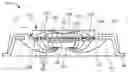
Referring now to FIG. 1, therein is shown a top view of an integrated circuit package system 100 in a first embodiment of the present invention. The integrated circuit package system 100 is shown having an encapsulation 102 such as an epoxy mould compound. The encapsulation 102 has an encapsulation edge 104.
At the edge 104 of the encapsulation 102 are leads 106. The leads 106 do not extend substantially beyond the edge 104 of the encapsulation 102. The encapsulation 102 fills spaces 108 in between the leads 106.
A second device 110 such as a wafer level chip scale package (WLCSP), a redistributed line (RDL) die, or an area array package is shown mounted above the encapsulation 102. Around an outer edge 112 of the second device 110 is a recess 114. The second device 110 is mounted inside the recess 114.
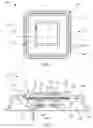
Referring now to FIG. 2, therein is shown a cross-sectional view of the integrated circuit package system 100 along the line 2-2 of FIG. 1. The integrated circuit package system 100 is shown having first device 202 such as a wire-bonded die. The first device 202 has an active side 204.
The active side 204 of the first device 202 is connected to interconnection pads 206. The interconnection pads 206 are coated or composed substantially of NiPd—Au. This nickel palladium and gold composition resists copper etching and allows the formation of the recess 114.
It has been unexpectedly discovered that the use of the interconnection pads 206 enables an electrical connection of the first device 202 without added structural elements such as interposers and substrates. This allows for a very thin package by reducing the number of internal components.
The active side 204 of the first device 202 is connected to the interconnection pads 206 with bond wires 208. The encapsulation 102 encapsulates the bond wires 208. The encapsulation also adds structural support by filling spaces 210 in between the interconnection pads 206.
The first device 202 is attached to a die pad 212 with die attach adhesive 214. The die pad is coated or composed substantially of NiPd—Au. The die attach adhesive 214 should be a high thermally conductive adhesive to allow the first device 202 to shed heat through the die pad 212.
The encapsulation 102 forms a rigid structure around the interconnection pads 206, the bond wires 208, and the first device 202. It has been unexpectedly discovered that the use of the encapsulation 102 as a rigid structure containing and supporting the interconnection pads 206, the bond wires 208, and the first device 202, reduces the complexity and number of internal components. The result being higher end-line yields, reduced costs, and competitive reduction in package size.
The encapsulation 102 also partially contains and partially surrounds the leads 106. The leads 106 are coated or composed substantially of NiPd—Au. The leads 106 are encapsulated by a top surface 220 of the encapsulation 102.
The leads 106 are connected to the interconnection pads 206 with the bond wires 208. The bond wires 208 are fully encapsulated by the encapsulation 102. Mounted in the recess 114, external to the encapsulation 102, is the second device 110.
The recess 114 further contributes to the thin dimensions of the package. Because of the absence of structural components such as interposers or substrates, the second device 110 may be mounted closer to the first device 202.
It has been unexpectedly discovered that mounting the first device 202 closer to the second device 110 reduces parasitic inductance. The reduction in distance reduces the inductance generated in high-speed components that can reduce the performance of the package as a whole, thus increasing the operating parameters of the first device 202 and the second device 110.
The second device 110 is connected to the interconnection pads 206 with interconnects such as metal connection pads 222. The second device 110 is shown having a second wire-bonded die 224 with an active side 226.
The active side 226 is connected to the metal connection pads 222 with the bond wires 208. The wire-bonded die 224 is attached to a second die pad 228 with the die attach adhesive 214. Encapsulating the second wire-bonded die 224 is a second encapsulation 230.
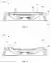
Referring now to FIG. 3, therein is shown the cross-sectional view of the integrated circuit package system 100 of FIG. 2 in a pre-etch phase of manufacture. The integrated circuit package system 100 is shown having a die attach paddle 302 such as a copper die attach paddle.
The die attach paddle 302 has the interconnection pads 206 connected to a bottom surface 304 of the die attach paddle 302. The die attach paddle 302 is exposed on the top surface 220 of the encapsulation 102. The NiPd—Au is resistant to Copper etching, which will leave the leads 106 and the interconnection pads 206 remaining after a copper etch has etched the die attach paddle 302. This result may also be accomplished by a selective etching only the die attach paddle 302 in the recess 114.
Referring now to FIG. 4, therein is shown the integrated circuit package system 100 of FIG. 2 in a post-etch phase of manufacture. The integrated circuit package system 100 is shown having the recess 114 created near the top surface of the encapsulation 102.
The interconnection pads 206 are now exposed in the recess 114. The encapsulation 102 between the spaces 210 of the interconnection pads 206 is also exposed.
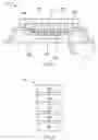
Referring now to FIG. 5, therein is shown a cross-sectional view of an integrated circuit package system 500 in a second embodiment of the present invention. The integrated circuit package system 500 is shown having first device 502 such as a flip chip. The first device 502 has an active side 504.
The active side 504 of the first device 502 is connected to interconnection pads 506. The interconnection pads 506 are coated or composed substantially of NiPd—Au. This nickel palladium and gold composition resists copper etching and allows the formation of a recess 508.
It has been unexpectedly discovered that the use of the interconnection pads 506 enables an electrical connection of the first device 502 without added structural elements such as interposers and substrates. This allows for a very thin package by reducing the number of internal components.
The active side 504 of the first device 502 is connected to the interconnection pads 506 with interconnects such as solder balls 512. An encapsulation 514, such as an epoxy mold compound, encapsulates the solder balls 512. The encapsulation also adds structural support by filling spaces 516 in between the interconnection pads 506.
The encapsulation 514 forms a rigid structure around the interconnection pads 506, the solder balls 512, and the first device 502. It has been unexpectedly discovered that the use of the encapsulation 514 as a rigid structure containing and supporting the interconnection pads 506, the solder balls 512, and the first device 502, reduces the complexity and number of internal components. The result being higher end-line yields, reduced costs, and competitive reduction in package size.
The encapsulation 514 also partially contains and partially surrounds leads such as leads 518. The leads 518 are coated or composed substantially of NiPd—Au. The leads 518 are exposed from a top surface 520 of the encapsulation 514.
The leads 518 are connected to the interconnection pads 506 with bond wires 524. The bond wires 524 are fully encapsulated by the encapsulation 514. Mounted in the recess 508, external to the encapsulation 514, is a second device 526 such as a wafer level chip scale package (WLCSP), a redistributed line (RDL) die, or an area array package.
The recess 508 further contributes to the thin dimensions of the package. Because of the absence of structural components such as interposers or substrates, the second device 526 may be mounted closer to the first device 502.
It has been unexpectedly discovered that mounting the first device 502 closer to the second device 526 reduces parasitic inductance. The reduction in distance reduces the inductance generated in high-speed components that can reduce the performance of the package as a whole, thus increasing the operating parameters of the first device 502 and the second device 526.
The second device 526 is connected to the interconnection pads 506 with the solder balls 512. Mounted above the second device 526 is a third device 528 such as a wafer level chip scale package (WLCSP), a redistributed line (RDL) die, or an area array package.
The third device 528 is connected to the leads 518 with the solder balls 512.
Referring now to FIG. 6, therein is shown a flow chart of a system 600 for manufacturing the integrated circuit package system 100 of FIG. 1 in an embodiment of the present invention. The system 600 includes providing a die attach paddle with interconnection pads connected to a bottom surface of the die attach paddle in a block 602; connecting a first device to the interconnection pads with a bond wire in a block 604; connecting a lead to the interconnection pad or to the first device in a block 606; encapsulating the first device and the die attach paddle with an encapsulation having a top surface in a block 608; and etching the die attach paddle leaving a recess in the top surface of the encapsulation in a block 610.
Thus, it has been discovered that the etched recess system of the present invention furnishes important and heretofore unknown and unavailable solutions, capabilities, and functional aspects for package on package configurations. The resulting processes and configurations are straightforward, cost-effective, uncomplicated, highly versatile, accurate, sensitive, and effective, and can be implemented by adapting known components for ready, efficient, and economical manufacturing, application, and utilization.
While the invention has been described in conjunction with a specific best mode, it is to be understood that many alternatives, modifications, and variations will be apparent to those skilled in the art in light of the aforegoing description. Accordingly, it is intended to embrace all such alternatives, modifications, and variations that fall within the scope of the included claims. All matters hithertofore set forth herein or shown in the accompanying drawings are to be interpreted in an illustrative and non-limiting sense.
Claims
1. An integrated circuit package system comprising:
providing a die attach paddle with interconnection pads connected to a bottom surface of the die attach paddle;
connecting a first device to the interconnection pads with a bond wire;
connecting a lead to the interconnection pad or to the first device;
encapsulating the first device and the die attach paddle with an encapsulation having a top surface, and the lead is exposed from the top surface; and
etching the die attach paddle leaving a recess in the top surface of the encapsulation.
2. (canceled)
3. The system as claimed in claim 1 further comprising:
encapsulating the lead by the top surface of the encapsulation.
4. The system as claimed in claim 1 further comprising:
attaching a third device to the leads exposed from the top surface of the encapsulation.
5. The system as claimed in claim 1 wherein:
connecting the first device includes connecting a wire-bonded die or connecting a flip chip.
6. An integrated circuit package system comprising:
providing a die attach paddle with interconnection pads connected to a bottom surface of the die attach paddle;
connecting a first device to the interconnection pads with a bond wire;
connecting a second device to the interconnection pads with an interconnect;
connecting a lead that is coated or composed substantially of nickel, palladium, and gold to the interconnection pad or to the first device;
encapsulating the first device and the die attach paddle with an encapsulation having a top surface; and
etching the die attach paddle leaving a recess in the top surface of the encapsulation.
7. The system as claimed in claim 6 wherein:
connecting the second device with the interconnect includes connecting the second device with metal connection pads or with solder balls.
8. The system as claimed in claim 6 wherein:
providing the die attach paddle with the interconnection pads includes providing interconnection pads that are coated or composed substantially of nickel, palladium, and gold.
9. (canceled)
10. The system as claimed in claim 6 wherein:
connecting the second device includes mounting the second device inside the recess on the top surface of the encapsulation.
11. An integrated circuit package system comprising:
interconnection pads;
a first device mounted below the interconnection pads;
a bond wire, or a solder ball connecting the first device to the interconnection pads;
a lead connected to the interconnection pad or to the first device;
an encapsulation having a top surface encapsulating the first device, the lead is exposed from the top surface; and
a recess in the top surface of the encapsulation with the interconnection pads exposed therefrom.
12. (canceled)
13. The system as claimed in claim 11 wherein:
the lead is encapsulated by the top surface of the encapsulation.
14. The system as claimed in claim 11 further comprising:
a third device attached to the lead exposed from the top surface of the encapsulation.
15. The system as claimed in claim 11 wherein:
the first device is a wire-bonded die or a flip chip.
16. The system as claimed in claim 11 further comprising:
a second device mounted above the interconnection pads; and
an interconnect connecting the second device to the interconnection pads.
17. The system as claimed in claim 16 wherein:
a metal connection pad or with solder ball connects the second device to the interconnection pads.
18. The system as claimed in claim 16 wherein:
the interconnection pads are coated or composed substantially of nickel, palladium, and gold.
19. The system as claimed in claim 16 wherein:
the lead is coated or composed substantially of nickel, palladium, and gold.
20. The system as claimed in claim 16 wherein:
the second device is mounted inside the recess.
Images & Drawings included:
Sources:
- United States Patent and Trademark Office - verify current appl. status at the USPTO↗
Recent applications in this class:
- » 20250079272 2025-03-06
SEMICONDUCTOR DEVICE AND MANUFACTURING METHOD - » 20240332140 2024-10-03
LEAD FRAME AND SEMICONDUCTOR DEVICE - » 20240332139 2024-10-03
SEMICONDUCTOR DEVICE AND METHOD FOR MANUFACTURING SEMICONDUCTOR DEVICE - » 20240274512 2024-08-15
Semiconductor device including heat sink with exposed side from encapsulant and a method of manufacturing thereof - » 20240145353 2024-05-02
SEMICONDUCTOR MODULE, METHOD FOR MANUFACTURING SEMICONDUCTOR MODULE, SEMICONDUCTOR DEVICE, AND VEHICLE - » 20240105560 2024-03-28
SEMICONDUCTOR DEVICE AND MANUFACTURING METHOD OF SEMICONDUCTOR DEVICE - » 20240014106 2024-01-11
SEMICONDUCTOR DEVICE - » 20230395470 2023-12-07
Power module - » 20230386982 2023-11-30
Charging Base Lead Frame, Charging Base Lead Frame Assembly and Charging Base - » 20230343682 2023-10-26
SEMICONDUCTOR DEVICE
Recent applications for this Assignee:
- » 20160351486 2016-12-01
Semiconductor device and method of forming substrate including embedded component with symmetrical structure - » 20160300817 2016-10-13
Semiconductor device and method of forming a package in-fan out package - » 20160300797 2016-10-13
Double-sided semiconductor package and dual-mold method of making same - » 20160276307 2016-09-22
Semiconductor device and method of forming PoP semiconductor device with RDL over top package - » 20160276238 2016-09-22
Semiconductor device and method of forming supporting layer over semiconductor die in thin fan-out wafer level chip scale package - » 20160233168 2016-08-11
Semiconductor device and method of forming 3D dual side die embedded build-up semiconductor package - » 20160218089 2016-07-28
Semiconductor device and method of forming WLCSP with semiconductor die embedded within interconnect structure - » 20160214857 2016-07-28
Semiconductor device and method of forming MEMS package - » 20160197059 2016-07-07
Semiconductor device and method of forming shielding layer over integrated passive device using conductive channels - » 20160197022 2016-07-07
Semiconductor device and method of forming sacrificial adhesive over contact pads of semiconductor die