Method of joining electronic component and the electronic component
US20100244283A1
2010-09-30
12/728,555
2010-03-22
✅ Patent granted
US 8,304,338 B2
2012-11-06
-
-
Jarrett Stark | John M Parker
2030-08-26
Abstract:
Dummy electrodes (15) are disposed on wiring connected to first electrodes (2) of the substrate (1), outside a junction region containing all of the first electrodes (2) and second electrodes (6) and in bonding resin (4), the dummy electrodes (15) not being involved in electrical connection between the substrate (1) and the component (5). When conductive particles (3) in the bonding resin (4) are melted by heating, molten solder self-assembles and solidifies between the first electrodes (2) and the second electrodes (6) and on the dummy electrodes (15). With this configuration, the solder self-assembles between the adjacent dummy electrodes (15) and causes a solder short circuit. Thus it is possible to eliminate excessive solder supply between the adjacent first electrodes (2) and the adjacent second electrodes (6), thereby preventing short circuits between the adjacent first electrodes (2) and the adjacent second electrodes (6).
Assignee:
- PANASONIC CORPORATION 20,737 🇯🇵 Osaka, Japan
Interested in similar patents?
Get notified when new applications in this technology area are published.
Classification:
H01L2924/014 » CPC further
Indexing scheme for arrangements or methods for connecting or disconnecting semiconductor or solid-state bodies as covered by; Alloys Solder alloys
H01L2924/00 » CPC further
Indexing scheme for arrangements or methods for connecting or disconnecting semiconductor or solid-state bodies as covered by
H01L2924/0132 » CPC further
Indexing scheme for arrangements or methods for connecting or disconnecting semiconductor or solid-state bodies as covered by; Alloys Binary Alloys
H01L2924/0105 » CPC further
Indexing scheme for arrangements or methods for connecting or disconnecting semiconductor or solid-state bodies as covered by; Chemical elements Tin [Sn]
H01L2924/0665 » CPC further
Indexing scheme for arrangements or methods for connecting or disconnecting semiconductor or solid-state bodies as covered by; Polymers Epoxy resin
H01L2924/01083 » CPC further
Indexing scheme for arrangements or methods for connecting or disconnecting semiconductor or solid-state bodies as covered by; Chemical elements Bismuth [Bi]
H01L2924/00015 » CPC further
Indexing scheme for arrangements or methods for connecting or disconnecting semiconductor or solid-state bodies as covered by; Technical content checked by a classifier the subject-matter covered by the group, the symbol of which is combined with the symbol of this group, being disclosed as prior art
H05K3/3436 » CPC main
Apparatus or processes for manufacturing printed circuits; Assembling printed circuits with electric components, e.g. with resistor electrically connecting electric components or wires to printed circuits by soldering; Surface mounted components; Leadless components having an array of bottom contacts, e.g. pad grid array or ball grid array components
H01L23/49838 » CPC further
Details of semiconductor or other solid state devices; Arrangements for conducting electric current to or from the solid state body in operation, e.g. leads, terminal arrangements ; Selection of materials therefor consisting of soldered constructions; Leads, on insulating substrates, Geometry or layout
H01L24/11 » CPC further
Arrangements for connecting or disconnecting semiconductor or solid-state bodies; Methods or apparatus related thereto; Means for bonding being attached to, or being formed on, the surface to be connected, e.g. chip-to-package, die-attach, "first-level" interconnects; Manufacturing methods related thereto; Bump connectors ; Manufacturing methods related thereto Manufacturing methods
H01L24/29 » CPC further
Arrangements for connecting or disconnecting semiconductor or solid-state bodies; Methods or apparatus related thereto; Means for bonding being attached to, or being formed on, the surface to be connected, e.g. chip-to-package, die-attach, "first-level" interconnects; Manufacturing methods related thereto; Layer connectors, e.g. plate connectors, solder or adhesive layers; Manufacturing methods related thereto; Structure, shape, material or disposition of the layer connectors prior to the connecting process of an individual layer connector
H01L24/32 » CPC further
Arrangements for connecting or disconnecting semiconductor or solid-state bodies; Methods or apparatus related thereto; Means for bonding being attached to, or being formed on, the surface to be connected, e.g. chip-to-package, die-attach, "first-level" interconnects; Manufacturing methods related thereto; Layer connectors, e.g. plate connectors, solder or adhesive layers; Manufacturing methods related thereto; Structure, shape, material or disposition of the layer connectors after the connecting process of an individual layer connector
H01L24/83 » CPC further
Arrangements for connecting or disconnecting semiconductor or solid-state bodies; Methods or apparatus related thereto; Methods for connecting semiconductor or other solid state bodies using means for bonding being attached to, or being formed on, the surface to be connected using a layer connector
H01L24/92 » CPC further
Arrangements for connecting or disconnecting semiconductor or solid-state bodies; Methods or apparatus related thereto; Methods for connecting semiconductor or solid state bodies including different methods provided for in two or more of groups - Specific sequence of method steps
H01L24/16 » CPC further
Arrangements for connecting or disconnecting semiconductor or solid-state bodies; Methods or apparatus related thereto; Means for bonding being attached to, or being formed on, the surface to be connected, e.g. chip-to-package, die-attach, "first-level" interconnects; Manufacturing methods related thereto; Bump connectors ; Manufacturing methods related thereto; Structure, shape, material or disposition of the bump connectors after the connecting process of an individual bump connector
H01L2224/0554 » CPC further
Indexing scheme for arrangements for connecting or disconnecting semiconductor or solid-state bodies and methods related thereto as covered by; Means for bonding being attached to, or being formed on, the surface to be connected, e.g. chip-to-package, die-attach, "first-level" interconnects; Manufacturing methods related thereto; Bonding areas; Manufacturing methods related thereto; Structure, shape, material or disposition of the bonding areas prior to the connecting process of an individual bonding area External layer
H01L2224/05573 » CPC further
Indexing scheme for arrangements for connecting or disconnecting semiconductor or solid-state bodies and methods related thereto as covered by; Means for bonding being attached to, or being formed on, the surface to be connected, e.g. chip-to-package, die-attach, "first-level" interconnects; Manufacturing methods related thereto; Bonding areas; Manufacturing methods related thereto; Structure, shape, material or disposition of the bonding areas prior to the connecting process of an individual bonding area; External layer Single external layer
H01L2224/13099 » CPC further
Indexing scheme for arrangements for connecting or disconnecting semiconductor or solid-state bodies and methods related thereto as covered by; Means for bonding being attached to, or being formed on, the surface to be connected, e.g. chip-to-package, die-attach, "first-level" interconnects; Manufacturing methods related thereto; Bump connectors; Manufacturing methods related thereto; Structure, shape, material or disposition of the bump connectors prior to the connecting process of an individual bump connector; Core members of the bump connector Material
H01L2224/29 » CPC further
Indexing scheme for arrangements for connecting or disconnecting semiconductor or solid-state bodies and methods related thereto as covered by; Means for bonding being attached to, or being formed on, the surface to be connected, e.g. chip-to-package, die-attach, "first-level" interconnects; Manufacturing methods related thereto; Layer connectors, e.g. plate connectors, solder or adhesive layers; Manufacturing methods related thereto; Structure, shape, material or disposition of the layer connectors prior to the connecting process of an individual layer connector
H01L2224/838 » CPC further
Indexing scheme for arrangements for connecting or disconnecting semiconductor or solid-state bodies and methods related thereto as covered by; Methods for connecting semiconductor or other solid state bodies using means for bonding being attached to, or being formed on, the surface to be connected using a layer connector Bonding techniques
H01L2224/83886 » CPC further
Indexing scheme for arrangements for connecting or disconnecting semiconductor or solid-state bodies and methods related thereto as covered by; Methods for connecting semiconductor or other solid state bodies using means for bonding being attached to, or being formed on, the surface to be connected using a layer connector; Bonding techniques Involving a self-assembly process, e.g. self-agglomeration of a material dispersed in a fluid
H01L2924/01005 » CPC further
Indexing scheme for arrangements or methods for connecting or disconnecting semiconductor or solid-state bodies as covered by; Chemical elements Boron [B]
H01L2924/01006 » CPC further
Indexing scheme for arrangements or methods for connecting or disconnecting semiconductor or solid-state bodies as covered by; Chemical elements Carbon [C]
H01L2924/01012 » CPC further
Indexing scheme for arrangements or methods for connecting or disconnecting semiconductor or solid-state bodies as covered by; Chemical elements Magnesium [Mg]
H01L2924/01013 » CPC further
Indexing scheme for arrangements or methods for connecting or disconnecting semiconductor or solid-state bodies as covered by; Chemical elements Aluminum [Al]
H01L2924/01019 » CPC further
Indexing scheme for arrangements or methods for connecting or disconnecting semiconductor or solid-state bodies as covered by; Chemical elements Potassium [K]
H01L2924/01029 » CPC further
Indexing scheme for arrangements or methods for connecting or disconnecting semiconductor or solid-state bodies as covered by; Chemical elements Copper [Cu]
H01L2924/01033 » CPC further
Indexing scheme for arrangements or methods for connecting or disconnecting semiconductor or solid-state bodies as covered by; Chemical elements Arsenic [As]
H01L2924/01047 » CPC further
Indexing scheme for arrangements or methods for connecting or disconnecting semiconductor or solid-state bodies as covered by; Chemical elements Silver [Ag]
H01L2924/01078 » CPC further
Indexing scheme for arrangements or methods for connecting or disconnecting semiconductor or solid-state bodies as covered by; Chemical elements Platinum [Pt]
H01L2924/01079 » CPC further
Indexing scheme for arrangements or methods for connecting or disconnecting semiconductor or solid-state bodies as covered by; Chemical elements Gold [Au]
H01L2924/15788 » CPC further
Indexing scheme for arrangements or methods for connecting or disconnecting semiconductor or solid-state bodies as covered by; Details of package parts other than the semiconductor or other solid state devices to be connected; Die mounting substrate; Material with a principal constituent of the material being a non metallic, non metalloid inorganic material Glasses, e.g. amorphous oxides, nitrides or fluorides
H05K3/323 » CPC further
Apparatus or processes for manufacturing printed circuits; Assembling printed circuits with electric components, e.g. with resistor electrically connecting electric components or wires to printed circuits by conductive adhesives by applying an anisotropic conductive adhesive layer over an array of pads
H05K2201/09781 » CPC further
Indexing scheme relating to printed circuits covered by; Shape and layout; Shape and layout details of conductors covering at least two types of conductors provided for in - Dummy conductors, i.e. not used for normal transport of current; Dummy electrodes of components
H05K2201/09781 » CPC further
Indexing scheme relating to printed circuits covered by; Shape and layout; Shape and layout details of conductors covering at least two types of conductors provided for in - Dummy conductors, i.e. not used for normal transport of current; Dummy electrodes of components
H05K2201/10977 » CPC further
Indexing scheme relating to printed circuits covered by; Details of components or other objects attached to or integrated in a printed circuit board; Details of electrical connections of non-printed components, e.g. special leads; Other details of electrical connections Encapsulated connections
H05K2203/046 » CPC further
Indexing scheme relating to apparatus or processes for manufacturing printed circuits covered by; Soldering or other types of metallurgic bonding Means for drawing solder, e.g. for removing excess solder from pads
H05K2203/046 » CPC further
Indexing scheme relating to apparatus or processes for manufacturing printed circuits covered by; Soldering or other types of metallurgic bonding Means for drawing solder, e.g. for removing excess solder from pads
Y02P70/50 » CPC further
Climate change mitigation technologies in the production process for final industrial or consumer products Manufacturing or production processes characterised by the final manufactured product
Y02P70/50 » CPC further
Climate change mitigation technologies in the production process for final industrial or consumer products Manufacturing or production processes characterised by the final manufactured product
Y10T29/49117 » CPC further
Metal working; Method of mechanical manufacture; Electrical device making Conductor or circuit manufacturing
H01L2224/73204 » CPC further
Indexing scheme for arrangements for connecting or disconnecting semiconductor or solid-state bodies and methods related thereto as covered by; Means for bonding being of different types provided for in two or more of groups; Location after the connecting process on the same surface; Bump and layer connectors the bump connector being embedded into the layer connector
H01L2224/29099 » CPC further
Indexing scheme for arrangements for connecting or disconnecting semiconductor or solid-state bodies and methods related thereto as covered by; Means for bonding being attached to, or being formed on, the surface to be connected, e.g. chip-to-package, die-attach, "first-level" interconnects; Manufacturing methods related thereto; Layer connectors, e.g. plate connectors, solder or adhesive layers; Manufacturing methods related thereto; Structure, shape, material or disposition of the layer connectors prior to the connecting process of an individual layer connector; Core members of the layer connector Material
H01L2924/00013 » CPC further
Indexing scheme for arrangements or methods for connecting or disconnecting semiconductor or solid-state bodies as covered by; Technical content checked by a classifier Fully indexed content
H01L2224/05599 » CPC further
Indexing scheme for arrangements for connecting or disconnecting semiconductor or solid-state bodies and methods related thereto as covered by; Means for bonding being attached to, or being formed on, the surface to be connected, e.g. chip-to-package, die-attach, "first-level" interconnects; Manufacturing methods related thereto; Bonding areas; Manufacturing methods related thereto; Structure, shape, material or disposition of the bonding areas prior to the connecting process of an individual bonding area; External layer Material
H01L2224/0555 » CPC further
Indexing scheme for arrangements for connecting or disconnecting semiconductor or solid-state bodies and methods related thereto as covered by; Means for bonding being attached to, or being formed on, the surface to be connected, e.g. chip-to-package, die-attach, "first-level" interconnects; Manufacturing methods related thereto; Bonding areas; Manufacturing methods related thereto; Structure, shape, material or disposition of the bonding areas prior to the connecting process of an individual bonding area; External layer Shape
H01L2924/00014 » CPC further
Indexing scheme for arrangements or methods for connecting or disconnecting semiconductor or solid-state bodies as covered by; Technical content checked by a classifier the subject-matter covered by the group, the symbol of which is combined with the symbol of this group, being disclosed without further technical details
H01L2224/0556 » CPC further
Indexing scheme for arrangements for connecting or disconnecting semiconductor or solid-state bodies and methods related thereto as covered by; Means for bonding being attached to, or being formed on, the surface to be connected, e.g. chip-to-package, die-attach, "first-level" interconnects; Manufacturing methods related thereto; Bonding areas; Manufacturing methods related thereto; Structure, shape, material or disposition of the bonding areas prior to the connecting process of an individual bonding area; External layer Disposition
H01L23/28 IPC
Details of semiconductor or other solid state devices Encapsulations, e.g. encapsulating layers, coatings, e.g. for protection
H01R43/00 IPC
Apparatus or processes specially adapted for manufacturing, assembling, maintaining, or repairing of line connectors or current collectors or for joining electric conductors
H01L21/44 IPC
Processes or apparatus adapted for the manufacture or treatment of semiconductor or solid state devices or of parts thereof; Manufacture or treatment of semiconductor devices or of parts thereof the devices having at least one potential-jump barrier or surface barrier, e.g. PN junction, depletion layer or carrier concentration layer the devices having semiconductor bodies not provided for in groups, , , and with or without impurities, e.g. doping materials Manufacture of electrodes on semiconductor bodies using processes or apparatus not provided for in groups -
Description
FIELD OF THE INVENTION
The present invention relates to a method of joining an electronic component by which the component is mounted on a substrate by using the self-assembly of conductive particles such as solder powder contained in bonding resin.
BACKGROUND OF THE INVENTION
A known technique for joining a circuit board and an electronic component is “solder self-assembly” using “particle agglomeration to junction electrodes by a liquid surface tension”.
Referring to FIGS. 17A to 17E, the solder self-assembly as disclosed in Japanese Patent No. 3955302 and so on will be described below.
In order to join a component 5 to electrodes 2 formed on a circuit board 1 as shown in FIG. 17E, bonding resin 4 containing solder powder 3 is supplied onto the electrodes 2 formed on the circuit board 1 as shown in FIG. 17A. As shown in FIGS. 18A and 18B, the electrodes 2 are formed in an area layout so as to be opposed to electrodes 6 of the component 5 to be joined.
The bonding resin 4 is supplied by typical supply methods of viscous materials. The supply methods include dispensing, screen printing, and transfer. As shown in FIGS. 19A and 19B, the bonding resin 4 is supplied over the electrodes 2 on the circuit board 1.
In FIG. 17B, the component 5 is held by a suction tool 7 above the circuit board 1 placed on a stage 9. The electrodes 6 are positioned in opposition to the electrodes 2, and the component 5 is held with a gap H between the electrodes 2 and the electrodes 6. In this state, at least one of a heater 8 provided in the suction tool 7 and a heater 10 provided in the stage 9 is operated to heat at least one of the component 5 and the circuit board 1 with a predetermined temperature profile, so that the solder powder 3 in the bonding resin 4 melts as shown in FIG. 17C. Further, in the gap H between the electrodes 2 and the electrodes 6 and around the gap H, convection Z is formed by molten solder 12, which is the agglomeration of the molten solder powder 3, and the resin components of the bonding resin 4, so that the molten solder 12 self-assembles between the electrodes 2 and the electrodes 6 due to particle agglomeration to the electrodes by a liquid surface tension.
After that, the circuit board 1 and the component 5 are cooled to the melting point of the solder powder 3 or lower, so that as shown in FIG. 17D, the molten solder 12 self-assembled between the electrodes 2 and the electrodes 6 solidifies and solder metal joints 13 are made between the electrodes 2 and the electrodes 6.
Reference numeral 11 denotes the resin components of the cured bonding resin 4. The resin components act as an underfill for protecting the junctions between the component 5 and the circuit board 1 and obtaining a bonding strength after the solder joints are made.
DISCLOSURE OF THE INVENTION
However, when specific electrodes, for example, electrodes in an area layout are joined, molten solder may excessively assemble on the outermost electrodes and cause a solder short circuit, resulting in unstable fabrication of a product.
To be specific, FIG. 21A is a cross sectional view showing the electrodes in an area layout. FIG. 21B is a plan view of the joints of the electrodes. As shown in FIGS. 21A and 21B, solder short circuits 14 are caused by excessively self-assembling solder on the outermost electrodes in the area layout after joining.
FIG. 20A shows that the bonding resin 4 is supplied over the electrodes 2 formed in the area layout on the circuit board 1. The solder powder 3 is evenly dispersed in the supplied bonding resin 4.
Next, as shown in FIG. 20B, the component 5 is held and heated to melt the solder powder 3 while keeping the gap between the electrodes 2 and the electrodes 6. Further, the convection Z is formed by the molten solder 12 and the resin components of the bonding resin 4, so that the solder powder 3 flows as shown in FIG. 20C.
Of the electrodes 2 formed in the area layout on the circuit board 1, in the case of an inner electrode, for example, an electrode b in FIG. 20C, the solder powder 3 in an area B is likely to self-assemble in a joining process. The area B is obtained by uniformly dividing distances from the adjacent electrodes with the electrode b placed at the center of the area B.
As a result, of the electrodes formed in the area layout, the inner electrodes b other than the outermost electrodes each have the uniform area B obtained by uniformly dividing distances from the adjacent electrodes with the electrode b placed at the center of the area B. Thus substantially equal amounts (equal volumes) of the solder powder 3 are likely to assemble on the electrodes b.
In the case of an outermost electrode a, the self-assembling solder powder 3 is present in a large area A containing the bonding resin 4 having been supplied outside the outermost electrodes.
This is because in a path Z where solder particles melt and flow, the outermost electrode a does not have any other electrodes on which molten solder wets and stays. Consequently, the outermost electrode a inevitably has a larger amount (volume) of self-assembling solder than the inner electrode b in the area layout.
In generally used material supply methods including dispensing and printing for viscous materials, it is quite difficult to equalize an amount of the solder powder 3 in the area A with an amount of the solder powder 3 in the area B, that is, to control the amount of the bonding resin 4 outside the electrodes of the area layout.
An object of the present invention is to provide a method of joining an electronic component by which a substrate and the component can be stably joined to each other by a solder self-assembly method without causing a short circuit.
A method of joining an electronic component according to the present invention, when bonding resin containing conductive particles is disposed between a substrate and the component, the bonding resin retained in a gap between the first electrodes of the substrate and the second electrodes of the component is heated and flows to cause the conductive particles melted between the first electrodes and the second electrodes to self-assemble, and then the substrate and the component are cooled to a temperature not higher than the solidification temperature of the conductive particles to mount the component on the substrate, the method including: arranging dummy electrodes on wiring connected to the first electrodes of the substrate, outside a junction region containing all of the first electrodes and the second electrodes and in the bonding resin, the dummy electrodes not being involved in electrical connection between the substrate and the component; and causing the conductive particles melted between the first electrodes and the second electrodes and on the dummy electrodes to self-assemble and solidify by a flow of the heated bonding resin.
A method of joining an electronic component according to the present invention, when bonding resin containing conductive particles is disposed between a substrate and the component, the bonding resin retained in a gap between the first electrodes of the substrate and the second electrodes of the component is heated and flows to cause the conductive particles melted between the first electrodes and the second electrodes to self-assemble, and then the substrate and the component are cooled to a temperature not higher than the solidification temperature of the conductive particles to mount the component on the substrate, the method including: arranging first dummy electrodes adjacent to the first electrodes and second dummy electrodes adjacent to the first dummy electrodes at shorter intervals than the first electrodes on the substrate, outside a junction region containing all of the first electrodes and the second electrodes and in the bonding resin, the first and second dummy electrodes being arranged as dummy electrodes not being involved in electrical connection between the substrate and the component; and causing the conductive particles melted between the first electrodes and the second electrodes and on the dummy electrodes to self-assemble and solidify by a flow of the heated bonding resin.
A method of joining an electronic component according to the present invention, when bonding resin containing conductive particles is disposed between a substrate and the component, the bonding resin retained in a gap between the first electrodes of the substrate and the second electrodes of the component is heated and flows to cause the conductive particles melted between the first electrodes and the second electrodes to self-assemble, and then the substrate and the component are cooled to a temperature not higher than the solidification temperature of the conductive particles to mount the component on the substrate, the method including: arranging dummy electrodes on wiring connected to the second electrodes of the component, outside a junction region containing all of the first electrodes and the second electrodes and in the bonding resin, the dummy electrodes not being involved in electrical connection between the substrate and the component; and causing the conductive particles melted between the first electrodes and the second electrodes and on the dummy electrodes to self-assemble and solidify by a flow of the heated bonding resin.
A method of joining an electronic component according to the present invention, when bonding resin containing conductive particles is disposed between a substrate and the component, the bonding resin retained in a gap between the first electrodes of the substrate and the second electrodes of the component is heated and flows to cause the conductive particles melted between the first electrodes and the second electrodes to self-assemble, and then the substrate and the component are cooled to a temperature not higher than the solidification temperature of the conductive particles to mount the component on the substrate, the method including: arranging first dummy electrodes adjacent to the second electrodes and second dummy electrodes adjacent to the first dummy electrodes at shorter intervals than the second electrodes on the component, outside a junction region containing all of the first electrodes and the second electrodes and in the bonding resin, the first and second dummy electrodes being arranged as dummy electrodes not being involved in electrical connection between the substrate and the component; and causing the conductive particles melted between the first and second electrodes and on the dummy electrodes to self-assemble and solidify by a flow of the heated bonding resin.
An electronic component of the present invention is obtained such that bonding resin containing conductive particles is disposed between a substrate and the component, the bonding resin retained in a gap between the first electrodes of the substrate and the second electrodes of the component is heated and flows to cause the conductive particles melted between the first electrodes and the second electrodes to self-assemble, and then the substrate and the component are cooled to a temperature not higher than the solidification temperature of the conductive particles to mount the component on the substrate, wherein dummy electrodes are formed on wiring connected to the first electrodes of the substrate, outside a junction region containing all of the first electrodes and the second electrodes and in the bonding resin, the dummy electrodes not being involved in electrical connection between the substrate and the component.
An electronic component of the present invention is obtained such that bonding resin containing conductive particles is disposed between a substrate and the component, the bonding resin retained in a gap between the first electrodes of the substrate and the second electrodes of the component is heated and flows to cause the conductive particles melted between the first electrodes and the second electrodes to self-assemble, and then the substrate and the component are cooled to a temperature not higher than the solidification temperature of the conductive particles to mount the component on the substrate, wherein first dummy electrodes adjacent to the first electrodes and second dummy electrodes adjacent to the first dummy electrodes at shorter intervals than the first electrodes are formed on wiring connected to the first electrodes of the substrate, outside a junction region containing all of the first electrodes and the second electrodes and in the bonding resin, the first and second dummy electrodes being formed as dummy electrodes not being involved in electrical connection between the substrate and the component.
An electronic component of the present invention is obtained such that bonding resin containing conductive particles is disposed between a substrate and the component, the bonding resin retained in a gap between the first electrodes of the substrate and the second electrodes of the component is heated and flows to cause the conductive particles melted between the first electrodes and the second electrodes to self-assemble, and then the substrate and the component are cooled to a temperature not higher than the solidification temperature of the conductive particles to mount the component on the substrate, wherein dummy electrodes are formed on wiring connected to the second electrodes of the component, outside a junction region containing all of the first electrodes and the second electrodes and in the bonding resin, the dummy electrodes not being involved in electrical connection between the substrate and the component.
An electronic component of the present invention is obtained such that bonding resin containing conductive particles is disposed between a substrate and the component, the bonding resin retained in a gap between the first electrodes of the substrate and the second electrodes of the component is heated and flows to cause the conductive particles melted between the first electrodes and the second electrodes to self-assemble, and then the substrate and the component are cooled to a temperature not higher than the solidification temperature of the conductive particles to mount the component on the substrate, wherein first dummy electrodes adjacent to the second electrodes and second dummy electrodes adjacent to the first dummy electrodes at shorter intervals than the second electrodes are formed on the component, outside a junction region containing all of the first electrodes and the second electrodes and in the bonding resin, the first and second dummy electrodes being formed as dummy electrodes not being involved in electrical connection between the substrate and the component.
According to this configuration, the dummy electrodes are formed at proper locations on the substrate or the component. Thus by causing excessive molten conductive metal to self-assemble on the dummy electrodes, it is possible to eliminate a short circuit on the electrodes of the substrate and the electrodes of the component, thereby achieving mass production with stable quality.
BRIEF DESCRIPTION OF THE DRAWINGS
FIG. 1A is an enlarged plan view showing a circuit board used in a first embodiment of the present invention;
FIG. 1B is a plan view showing a state in which bonding resin is supplied to the circuit board used in the first embodiment;
FIG. 2 is an explanatory drawing showing the effect of dummy electrodes according to the first embodiment;
FIG. 3A is a horizontal sectional view showing excessive solder captured by the dummy electrodes according to the first embodiment;
FIG. 3B is a G-H sectional view showing the excessive solder captured by the dummy electrodes according to the first embodiment;
FIG. 3C is a J-K sectional view showing the excessive solder captured by the dummy electrodes according to the first embodiment;
FIG. 4 is an enlarged plan view showing the specific shapes of the dummy electrodes according to the first embodiment;
FIG. 5 is an enlarged plan view showing another specific shapes of the dummy electrodes according to the first embodiment;
FIG. 6A is an enlarged plan view showing still another specific shapes of the dummy electrodes before soldering according to the first embodiment;
FIG. 6B is an enlarged plan view showing the still another specific shapes of the dummy electrodes after soldering according to the first embodiment;
FIG. 7A is an enlarged plan view showing still another specific shapes of the dummy electrodes before soldering according to the first embodiment;
FIG. 7B is an enlarged plan view showing the still another specific shapes of the dummy electrodes after soldering according to the first embodiment;
FIG. 8A is an enlarged plan view of a circuit board of the prior art;
FIG. 8B is a plan view showing a state in which bonding resin is supplied to the circuit board of the prior art;
FIG. 9 is a plan view showing the occurrence of short circuits according to the prior art;
FIG. 10 is an explanatory drawing showing the mechanism of the occurrence of a short circuit according to the prior art;
FIG. 11 is an enlarged plan view showing a circuit board used in a second embodiment of the present invention;
FIG. 12 is an enlarged plan view showing the circuit board according to another specific example of the second embodiment;
FIG. 13 is an enlarged plan view showing the circuit board according to still another specific example of the second embodiment;
FIG. 14 is an enlarged plan view showing the circuit board according to still another specific example of the second embodiment;
FIG. 15 is an enlarged plan view showing the circuit board according to still another specific example of the second embodiment;
FIG. 16 is an enlarged plan view showing the circuit board according to still another specific example of the second embodiment;
FIG. 17 is an explanatory drawing showing a joining process according to “solder self-assembly method”;
FIG. 18A is an enlarged plan view showing a circuit board of the prior art;
FIG. 18B is an enlarged plan view showing a component;
FIG. 19A is a plan view showing a state in which bonding resin is supplied to the circuit board of the prior art;
FIG. 19B is a sectional view showing the state in which the bonding resin is supplied to the circuit board of the prior art;
FIG. 20A is an explanatory drawing showing “solder self-assembly method” and a mechanism for the circuit board of the prior art;
FIG. 20B is an explanatory drawing showing “solder self-assembly method” and the mechanism for the circuit board of the prior art;
FIG. 20C is an explanatory drawing showing “solder self-assembly method” and the mechanism for the circuit board of the prior art;
FIG. 21A is a sectional view showing a joining result of the prior art; and
FIG. 21B is a plan view showing the joining result of the prior art.
DESCRIPTION OF THE EMBODIMENTS
Referring to FIGS. 1A and 1B to 16, embodiments of the present invention will be described below.
First Embodiment
FIGS. 1A and 1B to 7A and 7B show a first embodiment of the present invention.
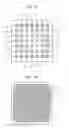
As shown in FIG. 1A, on a circuit board 1, 25 electrodes 2 are uniformly spaced in an area layout so as to be opposed to electrodes 6 of a component 5, and 24 dummy electrodes 15 not involved in electrical connection to the electrodes 6 of the component 5 are formed around the electrodes 2. As is evident from the size of the component 5 indicated by a virtual line in FIG. 1A, the component 5 has no electrodes corresponding to the dummy electrodes 15 provided on the side of the circuit board 1. The dummy electrodes 15 are hatched in distinction from the electrodes 2 of the circuit board 1 electrically connected to the electrodes 6 of the component 5.
As shown in FIG. 1B, bonding resin 4 is supplied over the dummy electrodes 15.
FIG. 1B schematically shows an example in which the bonding resin 4 is supplied over all the formed dummy electrodes 15. It is not always necessary to supply the bonding resin 4 over all the electrodes. The bonding resin 4 may flow to cover the dummy electrodes 15 in the subsequent joining process.
The circuit board 1 having the electrodes 2 and the dummy electrodes 15 and the component 5 having the electrodes 6 are aligned with each other such that the electrodes 2 and the electrodes 6 face each other. In a state in which a gap H is kept between the electrodes 2 and the electrodes 6, at least one of a heater 8 provided in a suction tool 7 and a heater 10 provided in a stage 9 is operated to heat at least one of the component 5 and the circuit board 1 with a predetermined temperature profile.
FIG. 2 shows a flowing behavior of solder powder 3 acting as conductive particles in the bonding resin 4 at this point.
Of the electrodes 2 formed in the area layout on the circuit board 1, in the case of an outermost electrode e, the solder powder 3 in an area E is likely to self-assemble in the joining process. The area E is obtained by uniformly dividing distances from the adjacent electrodes with the electrode e placed at the center of the area E.
The electrodes 2 other than the outermost electrode e each have the uniform area E obtained by uniformly dividing distances from the adjacent electrodes with the electrode 2 placed at the center of the area E. Thus substantially equal amounts (equal volumes) of the solder powder 3 are likely to self-assemble on the electrodes 2.
In the case of the dummy electrodes 15 formed outside the electrodes 2, for example, an electrode d in FIG. 2, the self-assembling solder powder 3 is present in a large area D containing the bonding resin 4 having been supplied outside the dummy electrodes 15.
This is because in a path Z where solder particles melt and flow, the outermost dummy electrode 15 does not have any other electrodes on which molten solder wets and stays. Consequently, the outermost electrode d inevitably has a larger amount (volume) of self-assembling solder than the inner electrode e.
Therefore, after the completion of joining in FIG. 3A, a larger amount of solder self-assembles on the dummy electrodes 15 than on the electrodes 2, so that as shown in FIGS. 3A and 3C, excessive solder is absorbed and thus solder short circuits 14 may occur at some points.
The dummy electrodes 15 absorb excessive solder thus, so that as shown in FIG. 3B, the electrodes 2 satisfactorily make solder metal joints 13 with the electrodes 6 with an equal amount of solder.
However, the dummy electrodes 15 on which excessive solder self-assembles are unnecessary electrodes in an electric circuit design. Thus even in the event of the solder short circuits 14, the electrical characteristics are not adversely affected.
FIG. 3A is a schematic drawing showing solder joints observed by X-rays from the above after joining. FIG. 3B is a sectional view taken along line G-H of FIG. 3A. FIG. 3C is a sectional view taken along line J-K of FIG. 3A.
Consequently, unlike in the prior art, the circuit board 1 and the component 5 can be stably joined to each other without causing solder short circuits on the outermost electrodes for joining in the area layout.
In FIGS. 1A and 1B to 3A, 3B, and 3C, the dummy electrodes 15 for absorbing excessive solder are formed on the circuit board 1. The present invention is not limited to this configuration. The dummy electrodes 15 may be formed on the side of the component 5.
FIGS. 1A and 1B to 3A, 3B, and 3C show the electrodes in the area layout. The present invention is not limited to this configuration. The electrodes may be peripherally arranged or other electrode layouts may be used.
Further, FIGS. 1A and 1B to 3A, 3B, and 3C show the dummy electrodes 15 not electrically connected to the electrodes 2 for joining. The present invention is not limited to this configuration. For example, the dummy electrodes 15 may be formed on a circuit pattern routed through the surface layer of the board from the electrodes 2 for joining in the area layout.
Example 1
The circuit board 1 of FIG. 1A was a glass epoxy board of grade FR4 and also a double-sided board having a thickness of 0.6 mm. On the circuit board 1, the 484 electrodes 2 to be joined to the electrodes 6 of the component 5 were arranged at intervals of 200 μm in the area layout. The electrode 2 was formed by plating Cu, which was 100 μm in diameter and 18 μm in height, with Ni/Au.
Further, around the electrodes 2, the dummy electrodes 15 for absorbing excessive solder were arranged at intervals of 200 μm with the same size as the electrodes 2.
As shown in FIG. 1B, the circuit board 1 and the component 5 were joined to each other by supplying the bonding resin 4 onto the electrodes 2 and the dummy electrodes 15 of the circuit board 1 under the following conditions:
The bonding resin 4 was made of a material with a composition ratio of 50 wt % of the solder powder 3 having an average particle diameter of 20 μm, 22 wt % of epoxy resin, 22 wt % of a hardener, 5 wt. % of an activator, and 1 wt % of an accelerator. The composition of the solder powder 3 was SnBi solder.
The component 5 was a semiconductor chip that was a square of side 5.02 mm with a thickness of 150 μm. On the active surface of the component 5, Au plated electrodes that were 12 μm in height and 100 μm in diameter were arranged in the area layout so as to face the electrodes 2 of the circuit board 1.
After 2.0 mg of the bonding resin 4 was supplied onto the circuit board 1 by a dispensing method, the gap H between the electrodes 2 of the circuit board 1 and the electrodes 6 of the component 5 was set at 20 μm as in the prior art shown in FIG. 17B. After that, the junction temperature was set at 200° C. by the suction tool 7 and the stage 9, and then the circuit board 1 and the component 5 were joined to each other.
Evaluations of 100 joints proved that the rate of occurrence of a solder short circuit was 0% in the junction area of the electrodes 2 and the electrodes 6, whereas on the outermost dummy electrodes 15, the rate of occurrence of a solder short circuit was 54%.
According to these results, it was evident that the effect of the dummy electrodes 15 can prevent solder short circuits on the electrodes 2 for joining.
Comparative Example 1
As a comparative experiment, joints were evaluated also on the circuit board 1 of the prior art shown in FIG. 18A, in which the dummy electrodes 15 for absorbing excessive solder are not provided.
On the circuit board 1, the 484 electrodes 2 were similarly arranged at intervals of 200 μm in the area layout. The electrodes 2 were 100 μm in diameter and 18 μm in height and were formed by plating Cu with Ni/Au. The component 5 was a semiconductor chip on which Au plated electrodes that were 12 μm in height and 100 μm in diameter were arranged in the area layout so as to face the electrodes 2 of the circuit board 1.
Evaluations of 100 joints proved that the rate of occurrence of the solder short circuit 14 was 75% only on the outermost electrodes 2 in FIG. 21B.
According to these results, it was evident that the dummy electrodes 15 provided outside the electrodes 2 can remarkably suppress solder short circuits on the junction electrodes.
As shown in FIG. 4, the dummy electrodes 15 have the same shape and size as the electrodes 2. The present invention is not limited to this configuration. To be specific, the dummy electrodes 15 may be different in shape and size from the electrodes 2. For example, the dummy electrodes 15 may be squares as shown in FIG. 5.
Moreover, the dummy electrodes 15 are formed at equal intervals in a row around the electrodes 2 in the area layout. The present invention is not limited to this configuration. To be specific, as shown in FIG. 6A, the dummy electrodes 15 may be formed in multiple rows. More specifically, around the electrodes 2 in the area layout, dummy electrodes 15a are arranged at intervals P1 like the electrodes 2. Further, dummy electrodes 15b are arranged at intervals P2, which are shorter than the intervals P1, around the dummy electrodes 15a in the single row such that the dummy electrodes 15b are each centered between the dummy electrodes 15a in a staggered arrangement. Thus the adjacent dummy electrodes 15a and 15b are spaced at intervals P3, which are shorter than the intervals P1 of the electrodes 2. When the circuit board 1 of FIG. 6A is soldered under the foregoing conditions, the solder short circuits 14 occur between the adjacent dummy electrodes 15a and 15b as shown in FIG. 6B, so that excessive solder is absorbed and the occurrence of solder short circuits is suppressed on the electrodes 2 in the area layout.
In FIGS. 4 to 6A, it is preferable to arrange similar numbers of the dummy electrodes 15 at equal intervals around the outermost electrodes of the electrodes 2 in the area layout. The present invention is not limited to this configuration. Any number of dummy electrodes may be formed at any positions to obtain the same effect.
In FIGS. 4 to 6A, the electrodes 2 for joining and the dummy electrodes 15 are not electrically connected to each other. The present invention is not limited to this configuration.
For example, as shown in FIG. 7A, the dummy electrodes 15 may be formed on a circuit pattern 16 routed through the board 1 from the electrodes 2 in the area layout. In this case, as shown in FIG. 7B, the solder short circuits 14 occurring between the dummy electrodes 15 absorb excessive solder, thereby suppressing solder short circuits on the electrodes 2 in the area layout. Moreover, in this case, the shapes of the dummy electrodes 15 are not limited and thus the dummy electrodes 15 may have any shapes. Instead of the single line arrangement of FIG. 7A, the dummy electrodes 15 may have a staggered arrangement or may be alternately removed. Even when the dummy electrodes 15 are close to each other, solder attracted to the dummy electrodes 15 flows also into the circuit pattern 16 and wets the circuit pattern 16. Thus, a solder bridge hardly occurs and causes short circuits between the adjacent dummy electrodes 15. Specifically, in this case, a solder resist is not provided outside the junction area of the routed circuit pattern 16.
In the first embodiment, the dummy electrodes 15 are provided on the circuit board 1. The dummy electrodes 15, 15a, and 15b may be provided on the component 5 to obtain the same effect.
Second Embodiment
Referring to FIGS. 11 to 16, a second embodiment of the present invention will be described below.
FIGS. 8A and 8B to 10 show the prior art in which electrodes 2 are arranged on the periphery of a circuit board 1.
First, the prior art will be described below for comparison.
The circuit board 1 of FIG. 8A was a glass epoxy board of grade FR4 and also a double-sided board having a thickness of 0.6 mm. On the circuit board 1, the 240 electrodes 2 to be joined to an electronic component were peripherally arranged at intervals of 150 μm. The substrate electrodes 2 were formed by plating Cu, which was 60 μm in width and 15 μm in height, with Ni/Au.
As shown in FIG. 8B, the circuit board 1 and a component 5 were joined to each other by supplying bonding resin 4 onto the electrodes 2 on the circuit board 1 under the following conditions:
The bonding resin 4 was made of a material with a composition ratio of 50 wt % of solder powder 3 having an average particle diameter of 20 μm, 22 wt % of epoxy resin, 22 wt % of a hardener, 5 wt % of an activator, and 1 wt % of an accelerator. The composition of the solder powder 3 was SnBi solder.
After 1.0 mg of the bonding resin 4 was supplied onto the circuit board 1 by a dispensing method, a gap H between the electrodes 2 of the circuit board 1 and electrodes 6 of the component 5 was set at 20 μm as in the prior art shown in FIG. 17B. After that, the junction temperature was set at 200° C. by a suction tool 7 and a stage 9, and then the circuit board 1 and the component 5 were joined to each other.
The component 5 was a semiconductor element having a thickness of 400 μm. On the active surface of the component 5, Au plated electrodes that were 12 μm in height and 60 μm in diameter were peripherally arranged so as to face the electrodes 2 of the circuit board 1.
Evaluations of 100 joints proved that the rate of occurrence of a solder short circuit 14 in FIG. 9 was 64% on the electrodes 2. FIG. 9 is a schematic drawing showing the solder joints of the electronic component and the circuit board, the solder joints being observed by X-rays.
In this example of joining, in a process of joining the electrodes 2 peripherally arranged on the circuit board 1 as shown in FIG. 10, the solder powder 3 in an area F is likely to self-assemble for, for example, an electrode f. The area F is obtained by uniformly dividing distances from the adjacent electrodes with the electrode f placed at the center of the area F, and the area F widely includes the inner and outer sides of the electrode f peripherally arranged on the circuit board 1. Since a flow path Z does not have any other electrodes on which solder wets, the solder powder 3 widely distributed inside and outside the peripherally arranged electrode f assembles with a larger solder amount than necessary for joining. It is estimated that the solder is excessively supplied for this reason and causes a solder short circuit.
In the second embodiment of the present invention, as shown in FIG. 11, joints were evaluated using a substrate on which dummy electrodes 15 for absorbing excessive solder were uniformly spaced inside and outside electrodes 2 peripherally arranged on a circuit board 1. The dummy electrodes 15 had the same size as the electrodes 2 and were made of the same material as the electrodes 2.
As a result of evaluations of 100 joints under completely the same process conditions as the joints of the substrate electrode configuration shown in FIG. 8A, the rate of occurrence of a solder short circuit was 0%.
This result proved that also in the electrode configuration of a peripheral arrangement, the dummy electrodes 15 for absorbing excessive solder inside and outside the electrodes 2 considerably suppress solder short circuits on junction electrodes.
As shown in FIG. 11, the dummy electrodes 15 of the same size and shape are formed inside and outside the peripherally arranged electrodes 2. The present invention is not limited to this configuration. The dummy electrodes 15 may be provided only on one side of the peripherally arranged electrodes as shown in FIGS. 12 and 13 or the dummy electrodes 15 may be formed inside and outside the electrodes in a mixed manner according to the size of an object to be joined, a bonding pitch, and a circuit pattern design. Further, the shapes and the number of dummy electrodes 15 may be optionally determined according to an object.
As shown in FIG. 14, the dummy electrodes 15 may be formed on a circuit pattern 16 of the peripherally formed electrodes 2. The circuit pattern 16 is routed through the surface layer of the substrate. The shapes of the dummy electrodes 15 on the circuit pattern 16 are not particularly limited and thus the dummy electrodes 15 may have any shapes at any positions. Even when the dummy electrodes 15 are close to each other, solder attracted to the dummy electrodes 15 flows also into the circuit pattern 16 and wets the circuit pattern 16. Thus, a solder bridge hardly occurs and causes a short circuit between the adjacent dummy electrodes 15. Specifically, in this case, a solder resist is not provided outside the junction area of the routed circuit pattern 16.
Further, as shown in FIGS. 15 and 16, at least one large dummy electrode 15 for absorbing excessive solder may be formed inside the peripherally arranged junction electrodes 2.
Also in the second embodiment, the dummy electrodes 15 for absorbing excessive solder may be provided on the component 5 instead of the circuit board 1 to obtain the same effect.
In the foregoing embodiments, the conductive particles contained in the bonding resin 4 are the solder powder 3. Moreover, solder coating copper powder, solder coating silver powder, and conductive particles such as metal particles coated with a low-melting metal are similarly usable as the conductive particles.
The present invention can contribute to improvement in quality of connection between the electrodes of a semiconductor chip, which is used for electronic equipment having been reduced in size and weight and has a small and fine electrode pitch, and the electrodes of a printed circuit board on which a fine wiring pattern is formed.
Claims
What is claimed is:1. A method of joining an electronic component, when bonding resin containing conductive particles is disposed between a substrate and the component, the bonding resin retained in a gap between first electrodes of the substrate and second electrodes of the component is heated and flows to cause the conductive particles melted between the first electrodes and the second electrodes to self-assemble, and then the substrate and the component are cooled to a temperature not higher than a solidification temperature of the conductive particles to mount the component on the substrate,
the method comprising:
arranging dummy electrodes on wiring connected to the first electrodes of the substrate, outside a junction region containing all of the first electrodes and the second electrodes and in the bonding resin, the dummy electrodes not being involved in electrical connection between the substrate and the component; and
causing the conductive particles melted between the first electrodes and the second electrodes and on the dummy electrodes to self-assemble and solidify by a flow of the heated bonding resin.
2. A method of joining an electronic component, when bonding resin containing conductive particles is disposed between a substrate and the component, the bonding resin retained in a gap between first electrodes of the substrate and second electrodes of the component is heated and flows to cause the conductive particles melted between the first electrodes and the second electrodes to self-assemble, and then the substrate and the component are cooled to a temperature not higher than a solidification temperature of the conductive particles to mount the component on the substrate,
the method comprising:
arranging first dummy electrodes adjacent to the first electrodes and second dummy electrodes adjacent to the first dummy electrodes at shorter intervals than the first electrodes on the substrate, outside a junction region containing all of the first electrodes and the second electrodes and in the bonding resin, the first and second dummy electrodes being arranged as dummy electrodes not being involved in electrical connection between the substrate and the component; and
causing the conductive particles melted between the first electrodes and the second electrodes and on the dummy electrodes to self-assemble and solidify by a flow of the heated bonding resin.
3. A method of joining an electronic component, when bonding resin containing conductive particles is disposed between a substrate and the component, the bonding resin retained in a gap between first electrodes of the substrate and second electrodes of the component is heated and flows to cause the conductive particles melted between the first electrodes and the second electrodes to self-assemble, and then the substrate and the component are cooled to a temperature not higher than a solidification temperature of the conductive particles to mount the component on the substrate,
the method comprising:
arranging dummy electrodes on wiring connected to the second electrodes of the component, outside a junction region containing all of the first electrodes and the second electrodes and in the bonding resin, the dummy electrodes not being involved in electrical connection between the substrate and the component; and
causing the conductive particles melted between the first electrodes and the second electrodes and on the dummy electrodes to self-assemble and solidify by a flow of the heated bonding resin.
4. A method of joining an electronic component, when bonding resin containing conductive particles is disposed between a substrate and the component, the bonding resin retained in a gap between first electrodes of the substrate and second electrodes of the component is heated and flows to cause the conductive particles melted between the first electrodes and the second electrodes to self-assemble, and then the substrate and the component are cooled to a temperature not higher than a solidification temperature of the conductive particles to mount the component on the substrate,
the method comprising:
arranging first dummy electrodes adjacent to the second electrodes and second dummy electrodes adjacent to the first dummy electrodes at shorter intervals than the second electrodes on the component, outside a junction region containing all of the first electrodes and the second electrodes and in the bonding resin, the first and second dummy electrodes being arranged as dummy electrodes not being involved in electrical connection between the substrate and the component; and
causing the conductive particles melted between the first electrodes and the second electrodes and on the dummy electrodes to self-assemble and solidify by a flow of the heated bonding resin.
5. An electronic component obtained such that bonding resin containing conductive particles is disposed between a substrate and the component, the bonding resin retained in a gap between first electrodes of the substrate and second electrodes of the component is heated and flows to cause the conductive particles melted between the first electrodes and the second electrodes to self-assemble, and then the substrate and the component are cooled to a temperature not higher than a solidification temperature of the conductive particles to mount the component on the substrate,
wherein dummy electrodes are formed on wiring connected to the first electrodes of the substrate, outside a junction region containing all of the first electrodes and the second electrodes and in the bonding resin, the dummy electrodes not being involved in electrical connection between the substrate and the component.
6. The electronic component according to claim 5, wherein the component is one of a semiconductor chip, a flexible substrate, and a rigid substrate.
7. The electronic component according to claim 5, wherein the component is a semiconductor chip on which the second electrodes are peripherally arranged, and
the dummy electrodes are formed on at least one of an outer side and an inner side of the peripherally arranged second electrodes.
8. An electronic component obtained such that bonding resin containing conductive particles is disposed between a substrate and the component, the bonding resin retained in a gap between first electrodes of the substrate and second electrodes of the component is heated and flows to cause the conductive particles melted between the first electrodes and the second electrodes to self-assemble, and then the substrate and the component are cooled to a temperature not higher than a solidification temperature of the conductive particles to mount the component on the substrate,
wherein first dummy electrodes adjacent to the first electrodes and second dummy electrodes adjacent to the first dummy electrodes at shorter intervals than the first electrodes are formed on wiring connected to the first electrodes of the substrate, outside a junction region containing all of the first electrodes and the second electrodes and in the bonding resin, the first and second dummy electrodes being formed as dummy electrodes not being involved in electrical connection between the substrate and the component.
9. The electronic component according to claim 8, wherein the component is one of a semiconductor chip, a flexible substrate, and a rigid substrate.
10. The electronic component according to claim 8, wherein the component is a semiconductor chip on which the second electrodes are peripherally arranged, and
the dummy electrodes are formed on at least one of an outer side and an inner side of the peripherally arranged second electrodes.
11. An electronic component obtained such that bonding resin containing conductive particles is disposed between a substrate and the component, the bonding resin retained in a gap between first electrodes of the substrate and second electrodes of the component is heated and flows to cause the conductive particles melted between the first electrodes and the second electrodes to self-assemble, and then the substrate and the component are cooled to a temperature not higher than a solidification temperature of the conductive particles to mount the component on the substrate,
wherein dummy electrodes are formed on wiring connected to the second electrodes of the component, outside a junction region containing all of the first electrodes and the second electrodes and in the bonding resin, the dummy electrodes not being involved in electrical connection between the substrate and the component.
12. The electronic component according to claim 11, wherein the component is one of a semiconductor chip, a flexible substrate, and a rigid substrate.
13. The electronic component according to claim 11, wherein the component is a semiconductor chip on which the second electrodes are peripherally arranged, and
the dummy electrodes are formed on at least one of an outer side and an inner side of the peripherally arranged second electrodes.
14. An electronic component obtained such that bonding resin containing conductive particles is disposed between a substrate and the component, the bonding resin retained in a gap between first electrodes of the substrate and second electrodes of the component is heated and flows to cause the conductive particles melted between the first electrodes and the second electrodes to self-assemble, and then the substrate and the component are cooled to a temperature not higher than a solidification temperature of the conductive particles to mount the component on the substrate,
wherein first dummy electrodes adjacent to the second electrodes and second dummy electrodes adjacent to the first dummy electrodes at shorter intervals than the second electrodes are formed on the component, outside a junction region containing all of the first electrodes and the second electrodes and in the bonding resin, the first and second dummy electrodes being formed as dummy electrodes not being involved in electrical connection between the substrate and the component.
15. The electronic component according to claim 14, wherein the component is one of a semiconductor chip, a flexible substrate, and a rigid substrate.
16. The electronic component according to claim 14, wherein the component is a semiconductor chip on which the second electrodes are peripherally arranged, and
the dummy electrodes are formed on at least one of an outer side and an inner side of the peripherally arranged second electrodes.
Images & Drawings included:


Sources:
- United States Patent and Trademark Office - verify current appl. status at the USPTO↗
Similar patent applications:
- » 20220069185
Electronic component joining method and joined structure - » 20130214033
METHOD FOR JOINING A FIRST ELECTRONIC COMPONENT AND A SECOND COMPONENT - » 20130258632
Joining sheet, electronic component, and producing method thereof - » 20130277092
JOINING SHEET, ELECTRONIC COMPONENT, AND PRODUCING METHOD THEREOF - » 20130307146
Mounting structure of electronic component with joining portions and method of manufacturing the same - » 20140079472
Paste for joining components of electronic modules, system and method for applying the paste - » 20110092101
METHOD FOR JOINING PLASTIC PARTS OF ELECTRIC OR ELECTRONIC COMPONENTS - » 20150043186
Joined structural body of members, joining method of members, and package for containing an electronic component - » 20130105205
JOINED STRUCTURAL BODY OF MEMBERS, JOINING METHOD OF MEMBERS, AND PACKAGE FOR CONTAINING AN ELECTRONIC COMPONENT - » 20190191566
Electronic assembly with a component arranged between two circuit carriers, and method for joining such an assembly
Recent applications in this class:
- » 20250120020 2025-04-10
SIGNAL TRACE TRANSITION FOR HIGH DATA RATE APPLICATIONS - » 20250081357 2025-03-06
INTERPOSER FOR TROUBLESHOOTING A BALL GRID ARRAY (BGA) DEVICE AND COUPLING THE BGA DEVICE TO A PRINTED CIRCUIT BOARD WITH LIMITED HEAT EXPOSURE - » 20250024608 2025-01-16
CIRCUIT STRUCTURE - » 20240414851 2024-12-12
PRINTED CIRCUIT BOARD FOR A REFLOW PROFILING PROCESS - » 20240324109 2024-09-26
SOLDER BARRIER CONTACT FOR AN INTEGRATED CIRCUIT - » 20240284603 2024-08-22
REMOVABLE LID FOR FLIP CHIP-BALL GRID ARRAY (FC-BGA) PACKAGES - » 20240244761 2024-07-18
PACKAGES WITH A SHORTEST DISTANCE BETWEEN PACKAGE CONNECTORS AND A SEATING PLANE OF AT LEAST 6 MILS - » 20230328895 2023-10-12
ELECTRONIC COMPONENT MOUNTING STRUCTURE AND METHOD FOR MANUFACTURING SAME - » 20230240020 2023-07-27
Integrated circuit device with edge bond dam - » 20230225060 2023-07-13
SOLDER PADS WITH CONCAVE EDGES FOR BALL GRID ARRAYS
Recent applications for this Assignee:
- » 20250038213 2025-01-30
SLURRY FOR NON-AQUEOUS ELECTROLYTE SECONDARY CELL, METHOD FOR MANUFACTURING SLURRY FOR NON-AQUEOUS ELECTROLYTE SECONDARY CELL, ELECTRODE FOR NON-AQUEOUS ELECTROLYTE SECONDARY CELL, AND NON-AQUEOUS ELECTROLYTE SECONDARY CELL - » 20230388751 2023-11-30
Information providing method and information providing apparatus - » 20230187624 2023-06-15
Positive electrode active material for lithium ion secondary battery and lithium ion secondary battery - » 20220368162 2022-11-17
POWER TRANSMISSION COIL, POWER TRANSMISSION DEVICE, AND UNDERWATER POWER SUPPLY SYSTEMS - » 20220345978 2022-10-27
NETWORK CONTROL DEVICE, NETWORK CONTROL SYSTEM, AND NETWORK CONTROL METHOD - » 20220345847 2022-10-27
Information collecting method, communication control apparatus, and information collector apparatus - » 20220317284 2022-10-06
SURVEILLANCE SYSTEM, AND SURVEILLANCE METHOD - » 20220299596 2022-09-22
MONITORING DEVICE AND MONITORING METHOD - » 20220278402 2022-09-01
RECTANGULAR SECONDARY BATTERY - » 20220205908 2022-06-30
Cellulose composite determination method and apparatus for composite resin